EP0180793A1 - Disposition pour la conversion de mots codés à longueur variable en mots de données à longueur constante - Google Patents
Disposition pour la conversion de mots codés à longueur variable en mots de données à longueur constante Download PDFInfo
- Publication number
- EP0180793A1 EP0180793A1 EP85112736A EP85112736A EP0180793A1 EP 0180793 A1 EP0180793 A1 EP 0180793A1 EP 85112736 A EP85112736 A EP 85112736A EP 85112736 A EP85112736 A EP 85112736A EP 0180793 A1 EP0180793 A1 EP 0180793A1
- Authority
- EP
- European Patent Office
- Prior art keywords
- memory
- inputs
- data
- register
- bits
- Prior art date
- Legal status (The legal status is an assumption and is not a legal conclusion. Google has not performed a legal analysis and makes no representation as to the accuracy of the status listed.)
- Granted
Links
Images

Classifications
-
- H—ELECTRICITY
- H03—ELECTRONIC CIRCUITRY
- H03M—CODING; DECODING; CODE CONVERSION IN GENERAL
- H03M7/00—Conversion of a code where information is represented by a given sequence or number of digits to a code where the same, similar or subset of information is represented by a different sequence or number of digits
- H03M7/30—Compression; Expansion; Suppression of unnecessary data, e.g. redundancy reduction
-
- G—PHYSICS
- G06—COMPUTING OR CALCULATING; COUNTING
- G06F—ELECTRIC DIGITAL DATA PROCESSING
- G06F5/00—Methods or arrangements for data conversion without changing the order or content of the data handled
Definitions
- the invention relates to an arrangement according to the preamble of patent claim 1.
- variable-length coding When transmitting DPCM-coded color image components, variable-length coding is often used, which produces an irregular data flow.
- the maximum processing speed that is to say the operating clock frequency
- the memory register has as many memory locations as it corresponds to the smallest common multiple of the different word lengths of the code words and the data word
- the circuit complexity for the multiplexers and for the control of the write-in and read-out processes is simplified considerably.
- the processing speed is reduced again by converting the code words into data words which have a multiple of the final word width required. This is particularly important when coding television signals.
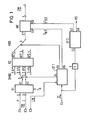
- the basic circuit diagram shown in FIG. 1 contains the series connection of a first register R1, a demultiplexer DMUX, a memory register R2, a data word multiplex device MUX and a FIRST IN / FIRST OUT memory (FIFO) ME.
- the preamble P of the code words and their information part I are present at the two inputs E1 and E2 of the first register.
- the corresponding outputs are labeled A1, A2.
- code words CW with two different lengths are present.
- the shorter code words have only the information part I of three bits in length, while the longer code words additionally have the preamble P with three bits.
- the bit combination of the preamble is not available in the information section.
- the demultiplexer DMUX has two inputs, each with three bits, and also two corresponding outputs, which can be connected as desired to the parallel inputs EP - here four inputs EP1 to EP4, each with three bits width - of the memory register R2.
- the memory register R2 has parallel outputs AP - here three outputs AP1 to AP3, each with a width of four bits, of which one output in each case via a multiplexer MUX to the data input E7 of the FIFO memory ME is switched on.
- Data words DW with a width of four bits are output at output A of the FIFO memory.
- Two controllers ST1 and ST2 are provided to control the demultiplexer D M UX, the data word multiplex device MUX and the FIFO memory ME.
- the first control ST1 is supplied with a length mode LM via an input E3, which specifies the length of the code words CW present.
- Both controls are started with a line pulse ZI at an input E4.
- the first controller ST1 controls the demultiplexer DMUX via its output A4, the data word multiplexing device MUX via its output A5 and the write-in clock TIN of the FIFO memory via output A6.
- the line pulse ZI passes through a delay circuit V to the input E5 of the second controller ST2, which delivers a constant readout clock T OUT to the read clock input E9 of the FIFO memory via its output A7 and further clocks and pulses M S for multiplexing at its output A8 with other signal components in the transmission of color signals and the necessary image pulses.
- a code word with a length of 6 bits applied to the outputs A1, A2 of the first register R1 is, as shown in FIG. 1, written into the memory register R2, for example, via the second and third inputs EP2, EP3.
- the next code word present at the output A2 of the first register R1 should have only three bits; this is written into the memory register R2 via the fourth input EP4.
- the next code word is then written in via the first input EP1 of the memory register, etc.
- the numbers on the connections between blocks each indicate the width the connecting bus.
- the first controller ST1 contains a counting device which indicates whether at least four bits have been written into the memory register R2. If this is the case, a data word with a width of four bits is read out of the memory register R2 via the data word multiplexing device MUX and written into the FIFO memory ME. The next four bits are then read out of the memory register R2 as a new data word.
- the memory register R2 must have as a minimum length the smallest common multiple of the different code word lengths and the word width of the data words read out, in this case thus 12 bits.
- a certain number of data words DW are first written into the FIFO memory ME before the first data word of this line is read out. This always ensures a continuous flow of data at the output A of the FIFO memory ME, even with frequently occurring code words of short length.
- the first control also ensures that a constant number of data words is written into the FIFO memory by reading empty combinations within each television line.
- the coding device connected upstream of this arrangement already ensures that long length code words do not occur too frequently and can cause the FIFO memory ME to overflow.
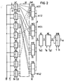
- the multiplexers M1 to M8 (74 LS 399 from Texas Instruments) contain memory stages which form the memory register R2. Inputs of the blocks that are not required are grounded, the outputs that are not required remain free.
- the memory register has 24 memory locations. This has the advantage that data bits eight bits wide are read out and written into the FIFO memory ME.
- the data word multiplexing device MUX contains four multiplexer modules Mll to M 14 (74 LS 153 from Texas Instruments), each with two data word multiplexers Mlll, Ml12 ... M142 with four (three required) inputs and one output. All outputs of the multiplexer modules Mll to M14 form an eight bit wide data bus which is connected via a sixth register R6 to the data input E7 of the FIFO memory ME (TDC 1030 from TRW, LSI Products Division, La Jolla, approx. 92038) , whose output is connected to the inputs of another M10 multiplexer with two four inputs and four output lines.
- TDC 1030 from TRW, LSI Products Division, La Jolla, approx. 92038
- Three bits of a code word are read into each of the multiplexers M1 to M8.
- the writing process is controlled via the associated select inputs S1 to S8 and the clock inputs CL1 to CLB.
- the first eight outputs of the memory registers forming three first multiplexer Ml to M3 are respectively connected to the first input EM1 of the eight data word multiplexer (MLLL to M142) of the four Multiplexerbausteine M ll to ML4.
- the first eight bit wide data word is read from the registers of the multiplexers M1 to M3 by connecting the first input EM1 of the data word multiplexers to the output via the interconnected select inputs SE of the data word multiplexers M111 to M142.
- the use of eight-bit data words has the advantage that the processing speed is reduced accordingly.
- the work clocks T A / 2 , T IN and T OUT fed to the sixth register and the FIFO memory have half the frequency of the work clock T A , with which data bits four bits wide are transmitted.
- the first control ST1 can be implemented as a read memory control.
- Three read memories EPROM, PRO M , ROM
- ROM1 to ROM3 module 74 S 288 from Texas Instr.
- the code words are buffered in the first register R1, so that they are delayed compared to the length mode LM.
- the outputs of the first read memory ROM1 are routed via a third register R3 and a downstream register R13 to the clock inputs CL1 to CL8 of the multiplexers M1 to M8.
- the third clock register R3 is supplied with the operating clock pulse T A present at the input E10 and the inverted operating clock pulse T A is fed to the downstream register R13.
- the outputs of the second read-only memory ROM2 are routed via a fourth register R4 to the select inputs S1 to S8 of the multiplexers M 1 to M 8.
- An output of the third read memory ROM3 is connected via a fifth register R5 to the interconnected select inputs SE of the multiplexer circuits M11 to M14.
- the third read memory ROM3 contains an adder AD.
- the associated data outputs A10 are connected to the input of the address register AR, to which the operating cycle T A is also fed.
- the inverted operating cycle T A is generated by an inverter IN.
- the output A9 of a binary counter Cl is connected to the input of an AND gate UN.
- Another input of the AND gate UN is connected to the fifth register R5; in addition, the work cycle T A is fed to the AND gate.
- the output of the AND gate UN supplies the write-in clock T IN for the FIFO memory ME and is also connected to the clock input of the binary counter C1.
- the reset inputs RE of the binary counter Cl and the address register AR are connected to the input E4.
- the address register AR and the binary counter B1 are set to a defined starting position.
- the selective inputs of the first multiplexer M1 and the second multiplexer M2 are first controlled via the second read memory RO M 2 and the fourth register R4, depending on the length mode LM.
- a code word comprising three bits is stored in the first multiplexer M1; a six-bit code word is stored in the first multiplexer M1 and the second multiplexer M2 in a controlled manner by the generated clock pulses CL1 or CL1 and CL2 generated by the third reter R3 and the downstream register R13.
- the binary counter C1 ensures that the same number of 4-bit data words is added to each television line by supplementation is written into the FIFO memory with empty combinations. If this predetermined number has been reached, the write-in pulses T IN are blocked via the output A9 of the binary counter C1 and via the AND gate UN. Since the original code words, which have a constant number for each television line, are reconstructed at the receiving end, any empty combinations can be used to fill up the FIFO memory ME.
- the reading of the television line begins with a delay. Accordingly, the image pulses must also be transmitted with a delay and the read-out process from the FIFO memory must also begin with a delay after the start of the first read-in process, for example after each picture change. This is achieved by the delay element V, which is connected upstream of the second control ST2. After the start of the reading process from the FIFO memory, the reading clock T OUT is continuously output by the control ST2. It is necessary to fill up the television lines with empty combinations, since reading and reading processes overlap on successive television lines.
- the second controller ST2 contains devices for the formation of the multiplex signals MS and for delaying the bidlim pulses which are essentially insignificant for the present invention, they need not be discussed further.
Landscapes
- Engineering & Computer Science (AREA)
- Theoretical Computer Science (AREA)
- Physics & Mathematics (AREA)
- General Engineering & Computer Science (AREA)
- General Physics & Mathematics (AREA)
- Compression, Expansion, Code Conversion, And Decoders (AREA)
- Time-Division Multiplex Systems (AREA)
- Radar Systems Or Details Thereof (AREA)
- Communication Control (AREA)
Priority Applications (1)
| Application Number | Priority Date | Filing Date | Title |
|---|---|---|---|
| AT85112736T ATE50074T1 (de) | 1984-10-12 | 1985-10-08 | Anordnung zur umsetzung von codewoertern mit unterschiedlicher laenge in datenwoerter gleicher laenge. |
Applications Claiming Priority (2)
| Application Number | Priority Date | Filing Date | Title |
|---|---|---|---|
| DE3437503 | 1984-10-12 | ||
| DE3437503 | 1984-10-12 |
Publications (2)
| Publication Number | Publication Date |
|---|---|
| EP0180793A1 true EP0180793A1 (fr) | 1986-05-14 |
| EP0180793B1 EP0180793B1 (fr) | 1990-01-31 |
Family
ID=6247775
Family Applications (1)
| Application Number | Title | Priority Date | Filing Date |
|---|---|---|---|
| EP85112736A Expired - Lifetime EP0180793B1 (fr) | 1984-10-12 | 1985-10-08 | Disposition pour la conversion de mots codés à longueur variable en mots de données à longueur constante |
Country Status (7)
| Country | Link |
|---|---|
| EP (1) | EP0180793B1 (fr) |
| JP (1) | JPS6195624A (fr) |
| AT (1) | ATE50074T1 (fr) |
| AU (1) | AU559000B2 (fr) |
| BR (1) | BR8505049A (fr) |
| DE (1) | DE3575800D1 (fr) |
| NO (1) | NO854054L (fr) |
Cited By (3)
| Publication number | Priority date | Publication date | Assignee | Title |
|---|---|---|---|---|
| JPS63196123A (ja) * | 1987-01-28 | 1988-08-15 | ドイチエ・トムソン−ブラント・ゲゼルシヤフト・ミツト・ベシユレンクテル・ハフツング | デジタル通信伝送方法および装置、デジタル記録および再生方法、デジタル再生装置 |
| DE3736898A1 (de) * | 1987-10-30 | 1989-05-11 | Siemens Ag | Anordnung zur umsetzung von codewoertern unterschiedlicher breite in datenwoerter gleicher breite |
| EP0905609A3 (fr) * | 1997-09-30 | 2000-04-05 | Siemens Aktiengesellschaft | Dispositif régistre |
Citations (1)
| Publication number | Priority date | Publication date | Assignee | Title |
|---|---|---|---|---|
| US4236206A (en) * | 1978-10-25 | 1980-11-25 | Digital Equipment Corporation | Central processor unit for executing instructions of variable length |
Family Cites Families (1)
| Publication number | Priority date | Publication date | Assignee | Title |
|---|---|---|---|---|
| JPS52105740A (en) * | 1976-03-01 | 1977-09-05 | Nippon Telegr & Teleph Corp <Ntt> | Buffer memory fead-out control system |
-
1985
- 1985-10-08 EP EP85112736A patent/EP0180793B1/fr not_active Expired - Lifetime
- 1985-10-08 DE DE8585112736T patent/DE3575800D1/de not_active Expired - Lifetime
- 1985-10-08 AT AT85112736T patent/ATE50074T1/de active
- 1985-10-09 JP JP60223899A patent/JPS6195624A/ja active Pending
- 1985-10-11 AU AU48509/85A patent/AU559000B2/en not_active Ceased
- 1985-10-11 NO NO854054A patent/NO854054L/no unknown
- 1985-10-11 BR BR8505049A patent/BR8505049A/pt unknown
Patent Citations (1)
| Publication number | Priority date | Publication date | Assignee | Title |
|---|---|---|---|---|
| US4236206A (en) * | 1978-10-25 | 1980-11-25 | Digital Equipment Corporation | Central processor unit for executing instructions of variable length |
Non-Patent Citations (4)
| Title |
|---|
| ELECTRONICS, Band 52, Nr. 2, Januar 1979, Seite 147; T.V. NHUYEN: "Selectors squeeze data into random-access memories" * |
| IBM TECHNICAL DISCLOSURE BULLETIN, Band 15, Nr. 8, Januar 1973, Seiten 2495-2496, New York, US; L.B. BAUMER: "Read-only memory controlled buffering" * |
| IBM TECHNICAL DISCLOSURE BULLETIN, Band 23, Nr. 2, Juli 1980, Seiten 791-795, New York, US; G.G. LANGDON: "High speed conversion between variable and fixed length words" * |
| NUCLEAR INSTRUMENTS AND METHODS, Band 131, Nr. 3, 28. Dezember 1975, Seiten 541-547, North-Holland Publishing Co., Amsterdam, NL; D.J. FEGAN: "A fast inexpensive 1024-Bit buffer memory data acquisition system for cosmic ray data using TTL integrated circuits and a paper tape punch" * |
Cited By (3)
| Publication number | Priority date | Publication date | Assignee | Title |
|---|---|---|---|---|
| JPS63196123A (ja) * | 1987-01-28 | 1988-08-15 | ドイチエ・トムソン−ブラント・ゲゼルシヤフト・ミツト・ベシユレンクテル・ハフツング | デジタル通信伝送方法および装置、デジタル記録および再生方法、デジタル再生装置 |
| DE3736898A1 (de) * | 1987-10-30 | 1989-05-11 | Siemens Ag | Anordnung zur umsetzung von codewoertern unterschiedlicher breite in datenwoerter gleicher breite |
| EP0905609A3 (fr) * | 1997-09-30 | 2000-04-05 | Siemens Aktiengesellschaft | Dispositif régistre |
Also Published As
| Publication number | Publication date |
|---|---|
| BR8505049A (pt) | 1986-07-29 |
| AU4850985A (en) | 1986-04-17 |
| ATE50074T1 (de) | 1990-02-15 |
| AU559000B2 (en) | 1987-02-19 |
| JPS6195624A (ja) | 1986-05-14 |
| DE3575800D1 (de) | 1990-03-08 |
| EP0180793B1 (fr) | 1990-01-31 |
| NO854054L (no) | 1986-04-14 |
Similar Documents
| Publication | Publication Date | Title |
|---|---|---|
| DE69323020T2 (de) | Dekodierer für veränderliche Längenkodes | |
| DE69128910T2 (de) | Digital-Analogwandler mit Wandlungsfehlerskompensation | |
| DE2754270C2 (fr) | ||
| DE3232600C2 (fr) | ||
| DE2819571A1 (de) | Datenverarbeitungsanlage mit mehreren prozessoren | |
| DE69329092T2 (de) | Huffman-Kode-Decodierungsschaltung | |
| DE69413512T2 (de) | Vorrichtung zur Dekodierung von Kodes mit veränderlicher Länge | |
| DE69130640T2 (de) | Arithmetische Operationseinheit mit Bit-Invertierungsfunktion | |
| DE2023693A1 (fr) | ||
| DE69125424T2 (de) | Vorrichtung zur variablen Längenkodierung und Vorrichtung zur variablen Längendekodierung | |
| DE3148099C2 (de) | Anordnung zum Erkennen einer Digitalfolge | |
| DE3340919A1 (de) | Datenprozessor | |
| EP0424554A1 (fr) | Convertisseur série-parallèle et/ou parallèle-série à plusieurs étages | |
| DE2543880A1 (de) | Anordnung zum verschluesseln und entschluesseln einer nachricht | |
| DE3406624C2 (fr) | ||
| DE3505314A1 (de) | Bitmusterwandler | |
| DE2848096C3 (de) | Digitale Addieranordnung | |
| DE69614763T2 (de) | Schaltung für schnellen Synchronzähler | |
| DE69016063T2 (de) | PCM-Übertragungssystem. | |
| EP0180793B1 (fr) | Disposition pour la conversion de mots codés à longueur variable en mots de données à longueur constante | |
| EP0732823A2 (fr) | Méthode de récupération d'horloge d'un signal numérique à la réception | |
| DE3044037A1 (de) | Verfahren und schaltung zur ratenaenderung | |
| EP0262731A2 (fr) | Circuit de transcodage de données | |
| DE2826454B2 (fr) | ||
| DE2636788B2 (de) | Datenspeicher für Datensichtgeräte |
Legal Events
| Date | Code | Title | Description |
|---|---|---|---|
| PUAI | Public reference made under article 153(3) epc to a published international application that has entered the european phase |
Free format text: ORIGINAL CODE: 0009012 |
|
| AK | Designated contracting states |
Kind code of ref document: A1 Designated state(s): AT BE CH DE FR GB IT LI NL SE |
|
| 17P | Request for examination filed |
Effective date: 19860707 |
|
| 17Q | First examination report despatched |
Effective date: 19880704 |
|
| GRAA | (expected) grant |
Free format text: ORIGINAL CODE: 0009210 |
|
| AK | Designated contracting states |
Kind code of ref document: B1 Designated state(s): AT BE CH DE FR GB IT LI NL SE |
|
| PG25 | Lapsed in a contracting state [announced via postgrant information from national office to epo] |
Ref country code: SE Effective date: 19900131 Ref country code: NL Effective date: 19900131 |
|
| REF | Corresponds to: |
Ref document number: 50074 Country of ref document: AT Date of ref document: 19900215 Kind code of ref document: T |
|
| REF | Corresponds to: |
Ref document number: 3575800 Country of ref document: DE Date of ref document: 19900308 |
|
| ET | Fr: translation filed | ||
| ITF | It: translation for a ep patent filed | ||
| GBT | Gb: translation of ep patent filed (gb section 77(6)(a)/1977) | ||
| NLV1 | Nl: lapsed or annulled due to failure to fulfill the requirements of art. 29p and 29m of the patents act | ||
| PG25 | Lapsed in a contracting state [announced via postgrant information from national office to epo] |
Ref country code: GB Effective date: 19901008 Ref country code: AT Effective date: 19901008 |
|
| PG25 | Lapsed in a contracting state [announced via postgrant information from national office to epo] |
Ref country code: LI Effective date: 19901031 Ref country code: CH Effective date: 19901031 Ref country code: BE Effective date: 19901031 |
|
| PLBE | No opposition filed within time limit |
Free format text: ORIGINAL CODE: 0009261 |
|
| STAA | Information on the status of an ep patent application or granted ep patent |
Free format text: STATUS: NO OPPOSITION FILED WITHIN TIME LIMIT |
|
| 26N | No opposition filed | ||
| BERE | Be: lapsed |
Owner name: SIEMENS A.G. Effective date: 19901031 |
|
| GBPC | Gb: european patent ceased through non-payment of renewal fee | ||
| PG25 | Lapsed in a contracting state [announced via postgrant information from national office to epo] |
Ref country code: FR Effective date: 19910628 |
|
| REG | Reference to a national code |
Ref country code: CH Ref legal event code: PL |
|
| PG25 | Lapsed in a contracting state [announced via postgrant information from national office to epo] |
Ref country code: DE Effective date: 19910702 |
|
| REG | Reference to a national code |
Ref country code: FR Ref legal event code: ST |