EP0181017A1 - Circuit pour simuler un transistor ou une diode - Google Patents
Circuit pour simuler un transistor ou une diode Download PDFInfo
- Publication number
- EP0181017A1 EP0181017A1 EP85201576A EP85201576A EP0181017A1 EP 0181017 A1 EP0181017 A1 EP 0181017A1 EP 85201576 A EP85201576 A EP 85201576A EP 85201576 A EP85201576 A EP 85201576A EP 0181017 A1 EP0181017 A1 EP 0181017A1
- Authority
- EP
- European Patent Office
- Prior art keywords
- voltage
- terminal
- circuit
- control
- coupled
- Prior art date
- Legal status (The legal status is an assumption and is not a legal conclusion. Google has not performed a legal analysis and makes no representation as to the accuracy of the status listed.)
- Granted
Links
Images


Classifications
-
- H—ELECTRICITY
- H03—ELECTRONIC CIRCUITRY
- H03D—DEMODULATION OR TRANSFERENCE OF MODULATION FROM ONE CARRIER TO ANOTHER
- H03D1/00—Demodulation of amplitude-modulated oscillations
- H03D1/14—Demodulation of amplitude-modulated oscillations by means of non-linear elements having more than two poles
- H03D1/18—Demodulation of amplitude-modulated oscillations by means of non-linear elements having more than two poles of semiconductor devices
-
- G—PHYSICS
- G01—MEASURING; TESTING
- G01R—MEASURING ELECTRIC VARIABLES; MEASURING MAGNETIC VARIABLES
- G01R19/00—Arrangements for measuring currents or voltages or for indicating presence or sign thereof
- G01R19/22—Arrangements for measuring currents or voltages or for indicating presence or sign thereof using conversion of AC into DC
-
- G—PHYSICS
- G06—COMPUTING OR CALCULATING; COUNTING
- G06G—ANALOGUE COMPUTERS
- G06G7/00—Devices in which the computing operation is performed by varying electric or magnetic quantities
- G06G7/48—Analogue computers for specific processes, systems or devices, e.g. simulators
- G06G7/62—Analogue computers for specific processes, systems or devices, e.g. simulators for electric systems or apparatus
Definitions
- the invention relates to a circuit in which current flow between first and second flow terminals thereof is controlled in response to an input voltage between a control terminal thereof and the second terminal, the circuit comprising:
- Such a circuit may act like a transistor or a semiconductor diode with shifted operational characteristics.
- Some electronic applications entail the use of current rectifiers whose optimum voltage properties cannot readily be achieved with an integral number of standard semiconductor rectifying elements. Circuits that simulate PN diodes but have shifted forward voltage characteristics are often employed in these applications.
- V BE refers to the voltage across the base-emitter junction of a bipolar transistor. When preceded by “standard”, this term means the base-to-emitter voltage of an NPN transistor when it just becomes forwardly conductive. Accordingly, the forward voltage across a conductive PN diode is about 1 standard V BE'
- the threshold voltage of a rectifier must exceed a standard "VBE but must not equal an exact number of (two or more) standard V BE 's.
- V BE multiplier in which the base of an NPN transistor is coupled to its collector through one resistor and to its emitter through another resistor.
- the V BE multiplier acts like a semiconductor diode whose forward conductive voltage equals a standard VBE multiplied by one plus the ratio of the resistor values.
- a simulated diode contains a PNP transistor connected to a transformer in such a manner that appropriate selection of the transformer turns ratio enables the threshold voltage of the diode to drop below a standard V BE .
- Gunn's simulated diode is, however, limited to AC operation.
- the transformer is not en element normally made in manufacturing integrated circuits. Modifying the manufacturing process to incorporate the transformer is difficult and costly. Providing the transformer as an element separate from an integrated circuit is unattractive. A circuit capable of acting as a rectifier with a forward voltage of less than a standard V BE for both AC and DC situations yet manufacturable with standard semiconductor elements is quite desirable.
- the circuit should be floating in the sense that its operation should not be restricted by a reference voltage.
- control point voltage is amplified by a gain set by the resistors to produce a control voltage for the main transistor. This downscales the forward voltage characteristics of the circuit. It can then become forwardly conductive at a voltage of lower magnitude than the transistor.
- the circuit may be characterized further in that the circuit comprises means for causing the voltage between the control electrode and the control point to differ by at least a selected voltage from that otherwise due to regulation of the voltage at the control point in response to the input voltage.
- the means act like a "floating battery" coupled between the first-mentioned node and the control electrode.
- the sign of the selected voltage is normally chosen so as to further downscale the forward voltage characteristics. The opposite sign may, however, be chosen. The voltage characteristics are then downscaled or upscaled depending on the magnitudes of the selected voltage and the gain.
- the circuit may be configured as a rectifying buffer by using a bipolar device for the main transistor. Its collector and emitter are the first and second electrodes through which (positive) current moves in a single flow direction during normal bipolar operation. Current at the control terminal also moves in a single flow direction when the input voltage is at a value sufficient to turn on the transistor. This configuration exhibits high input impedance and low output impedance.
- the circuit can simulate a diode by coupling the first terminal to the control terminal. Combining these two possibilities and suitably choosing the selected voltage enables the circuit to act like a diode having a forward voltage less than a standard V E E .
- the present circuit is highly accurate. It is manufacturable with normal semiconductor elements.
- the control system is preferably embodied with one or more amplifiers that utilize conventional semiconductor elements.
- the floating battery circuit portion which may be a separate semiconductor component or may be incorporated in the control system.
- a general transistor has a control electrode and a pair of flow electrodes through which current transmission is regulated by a control voltage, denoted here as V CI between the control electrode and one of the flow electrodes.
- V CI control voltage
- the variation of control voltage V c with current through the transistor depends on how it is fabricated and on the basic semiconductor properties of the transistor.
- the V c variation with current is particularly limited if the transistor is a bipolar device. For low-voltage applications, V C must often be small (in absolute value).
- V CS (V C - V A )/B (1)
- V A is a selected voltage that is approximately constant
- B is a constant greater than unity.
- Such a circuit acts like a conventional transistor except that the voltage characteristics are shifted according to Eq.(1).
- V CS , V C and V A are preferably all positive or all negative.
- V CS is therefore less than V C in absolute value. This is also true if V A is zero. That is, the voltage characteristics of the circuit are downscaled from those of the transistor responsive to voltage V C . For a given V c magnitude, the transistor reaches the same operational condition at a lower V CS magnitude.
- V A may, however, be of opposite sign to V C .
- the magnitudes of V A and B then determine whether V CS is larger or smaller than V c in absolute value at a given transistor current. That is, the voltage range of the circuit may be upscaled or downscaled. For certain magnitudes of V A and B, there is even a cross-over transistor current at which the voltage characteristics switch from being upscaled or downscaled.
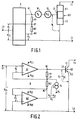
- Fig, 1 illustrates a three-terminal circuit that implements the adjusted voltage range of Eq. (1).
- This simulated transistor circuit has a high-impedance control terminal CT that receives an input voltage signal for controlling current flow between a pair of flow terminals T1 and T2.
- the input voltage is voltage V CS taken between terminals CT and T2.
- Transistor Q O may be a bipolar device or a field-effect transistor (FET) of either the insulated-gate or junction type.
- FET field-effect transistor
- electrodes CE, E1 and E2 are respectively the base, collector and emitter; V c is V BE .
- electrodes CE, E1 and E2 respectively are the gate, drain, and source; V c is the gate-to-source voltage.
- the factor B in Eq.(1) is provided by a pair of resistors R1 and R2 interconnected at a control point CP between respective nodes N1 and N2.
- the combination of resistors R1 and R2 amplifies the voltage at control point CP to produce an amplified voltage at node N1.
- a control system 8 regulates the voltage at point CP in response to input voltage V CS in such a manner that the CP voltage largely follows voltage V CS .
- the voltage V 1 between terminal CT and point CP is then near a specified (constant) value.
- Control system 8 supplies current at nodes N1 and N2 for resistors R1 and R2 and for the QO base which is coupled to node N1.
- control 8 provides (positive) current at node N1 and withdraws (positive) current at node N2. This is done without substantially affecting the currents at terminals T1 and T2.
- the voltage V 2 between terminal T2 and node N2 is likewise near a specified (constant) value.
- V A factor in Eq.(1) is provided by a portion of the circuit illustrated as a floating power supply (or battery) 10 in series with electrode CE. This circuit portion imposes voltage V A on the voltage that control system 8 otherwise causes to exist between point CP and electrode CE.
- V 12 is preferably set at V 20 + B(V 10 - V 20 ) where V 10 and V 20 are the respective constant components of V 1 and V 2 .
- V 10 and V 20 are typically a single circuit component implemented by other techniques.
- Control system 8 causes the CP voltage to increase when voltage V CS increases and vice versa without "drawing" significant current from transistor Q0.
- the CP voltage is amplified by factor B (set by resistors R1 and R2) and combined with voltage V A to produce voltage V C which controls transistor QO.
- the circuit then simulates a transistor responsive to voltage V CS .
- the circuit functions as a rectifier by simply interconnecting terminals CT and T1. Current then flows unidirectionally between terminal T2 and the joint T1/CT terminal. This occurs when the forward voltage V CS of the simulated diode reaches a threshold value determined by Eq. (1) from the QO conductive threshold.
- transistor QO becomes conductive only when current moves in a single flow direction at terminal CT. If transistor QO is a bipolar device whose emitter and collector are normally fixed (in contrast to an FET whose source and drain are often interchangeable), the circuit acts like a rectifying buffer with respect to the currents flowing at terminals CT and T2. Tying terminals CT and T1 together and suitably selecting the value of voltage V A (e.g., choosing V A to be zero or of the same sign tu lower magnitude than V c ) enables the circuit to simulate a PN diode whose forward voltage is less than a standard V BE .
- V A e.g., choosing V A to be zero or of the same sign tu lower magnitude than V c
- Fig. 2 illustrates a more particular embodiment of the circuit.
- transistor QO is an NPN transistor which turns on when its V BE reaches a standard V BE of 0.6 - 0.8 volt.
- Control system 8 consists of two- input high-gain amplifiers A1 and A2 that respectively function as a current source and a current sink for current through resistors R1 and R2.
- Amplifiers A1 and A2 are each connected between low and high voltage supplies V EE and V CC .
- Batteries 10 and 12 are implemented with a current supply 14 connected between point CP and a voltage supply V S .
- the V S supply voltage is more negative than the CP voltage (e.g. V s is V EE ) if (positive) current is to flow out of point CP to supply 14, and vice versa.
- amplifier A1 has non-inverting and inverting input terminals respectively connected to terminal CT and point CP. Voltage V 1 this occurs between the A1 input terminals.
- the A1 output terminal is connected to node N1 to provide current for elements R1, R2 and QO.
- the A2 output terminal is connected to node N2 to receive current from resistors R1 and R2.
- the output of amplifier A2 is also connected to its inverting input terminal, enabling amplifier A2 to be a voltage follower.
- Amplifier A2 has its non-inverting input terminal connected to terminal T2 so that voltage V 2 exists between its input terminals.
- Amplifiers A1 and A2 may be true operational amplifiers having high input impedances.
- the amplifier input currents are then very small compared to the R1 and R2 currents.
- Each voltage V 1 or V 2 consists of the associated amplifier input signal and an amplifier offset voltage (that results from non-ideal components).
- the constant components V 10 and V 20 are the corresponding A1 and A2 offset voltages which are ideally zero.
- the signal components of V 1 and V 2 are quite small. As a result, the voltages at point CP and terminal T2 are always very close to the respective voltages at terminal CT and node N2.
- amplifiers A1 and A2 may have (intentionally non-zero) input vias voltages.
- Each voltage V 1 or V 2 then consists of its input signal component, its voltage offset component, and its bias component.
- V 1 or V 21 its constant portion V 10 or V 20 equals the sum of its offset and bias components.
- the CP voltage thereby differs intentionally from voltage V CS but closely follows it.
- the T2 voltage differs from the N2 voltage by largely a constant amount.
- supply 14 provides a current of (V A + V 12 )/R 1 .
- This current flows through resistor R1 across which a voltage drop of V A + V 12 thereby occurs. This is in addition to the voltage drop due to the current sunk by amplifier A2 .
- a voltage drop of VA + V 12 also must occur along the path extending past node N1 through amplifier A1. This voltage is produced internally in amplifier A1 and is therefore not explicitly shown in Fig. 2.
- V BE The absolute value of V BE is approximately (kT/q)ln(I C /I S ), where k is Boltzmann's constant, T is the temperature, q is the electronic charge, I c is the collector current, and I S is the saturation current.
- Fig. 3 depicts a bipolar embodiment of Fig. 2 in which amplifiers A1 and A2 have input bias voltages.
- the A1 non-inverting and inverting inputs in Fig. 3 are respectively connected to the base and emitter of a PNP transistor Q1. Consequently, the input bias component of voltage V is about -1 standard VBE when transistor Q1 is fully conductive.
- the Q1 collector is connected to the emitter of an NPN transistor Q2 and also to one end of a resistor R3 whose other end is tied to the V EE supply.
- a reference voltage V R is supplied to the base of transistor Q2. Its collector drives an NPN transistor Q3 whose emitter is tied to the V EE supply.
- the Q3 oollector provides the A1 output signal to node N1.
- a capacitor C1 is connected between the Q3 collector and base to provide frequency compensation for amplifier A1.
- Current supplies 16, 18 and 20 are connected between the V CC supply on one hand and the Q1 emitter, the Q2 collector,
- the A2 non-inverting and inverting inputs are respectively connected to the base and emitter of a PNP transistor Q4.
- the V 2 input bias component is likewise about -1 standard V BE when transistor Q4 is fully on.
- NPN transistors Q5 and Q6, a resistor R4, and a compensating capacitor C2 in amplifier A2 are connected to each other and to transistor Q4 in the same way that elements Q2, Q3, R3 and C1 are respectively connected to each other and to transistor Q1.
- the Q6 collector provides the A2 output signal to node N2.
- a current supply 22 is connected between the V CC supply and the Q5 collector. Supply currents for transistors Q4 and Q6 are provided from resistor R2 by way of node N2.
- V A + V 12 is typically negative. This occurs because V A is normally less than 1 standard V BE while V 20 is about -1 standard V BE .
- Supply 14 is then implemented in Fig. 3 by simply choosing the value of current supply 16 to be
- the "excess" current from supply 16 flows through resistor R1 in the reverse direction to that which would cause a positive voltage drop from node N1 to point CP. Accordingly, negative voltage "V A + V12" occurs across resistor R1.
- the circuit of Fig. 3 operates as follows. Assume that voltage V CS is initially zero. The CP voltage is about 1 standard V BE above V CS . Transistor Q1 is highly conductive and provides its quiescent current to resistor R3. This raises the emitter voltage of transistor Q2 and causes it to be lowly conductive. The Q2 collector voltage is high, enabling transistor Q3 to be on. Transistor Q3 sinks the current from supply 20 plus the R1 current from supply 16, Transistor QO is off since the Q3 collector voltage is low. The QO V BE is zero at this point. Little current flows through resistor R2. Accordingly, transistors Q4 - Q6 are generally in the opposite respective conductive conditions to transistors Q1 - Q3.
- V CS As V CS rises above zero, V 1 increases slightly due to the A1 amplifying characteristic. However, the A1 amplification is sufficiently great that the V 1 change is not significant.
- the CP voltage therefore follows V CS upward.
- Transistor Q1 becomes less conductive, causing transistor Q2 to turn on harder so that transistor Q3 becomes less conductive. This diverts current from supply 20 to resistors R1 and R2 and the QO base. Due to the amplification set by resistors R1 and R2, V C rises more than V CS by factor B.
- Transistors Q4 - Q6 generally undergo opposite changes to those respectively occuring in transistors Q1 - Q3. Transistor Q6 now sinks appreciable current from resistor R2.
- Transistor QO turns on when its V BE reaches 1 standard V BE . The reverse occurs when V CS is later decreased.
- a significant feature of the circuit of Fig. 3 is that the QO emitter can reach low supply voltage V EE . This provides great flexibility in using the circuit.
- the power supply range (V CC - VEE) may be as low as 1 volt.
- resistors R1 and R2 are 5 and 10 kiloohms, respectively. B is thus 1.5. Resistor R3 or R4 is 11.3 kiloohms. Capacitor C1 or C2 is 4 picofarads. Supplies 16, 18, 20 and 22 are 46, 4, 34 and 4 microamperes, respectively. The Q1 or Q4 quiescent current is 4 microamperes.Factor V A is 0.4 volt. Correction V 12 is about -0.6 volt. Voltage V R is about 0.7 volt. Supplies V EE and V CC are 0 volt and 1 volt or more, respectively. Amplifiers A1 and A2 have amplifications of about 104.
- Fig. 4 shows curves indicating the performance of the foregoing embodiment. Each curve depicts the output current flowing between terminals T1 and T2 as a function of voltage. Curve 24 indicates the basic V BE characteristic of transistor Q O. Curve 26 shows how V CS would appear if V A were zero. Curve 28 represents how V CS would appear if B were unity. Finally, curve 30 shows how V CS varies when V A and B have the values given above.
- the circuits of Figs. 1 - 3 are especially useful in an envelope detector arranged as shown in Fig. 5 .
- This detector provides an output signal V OUT in the shape of the envelope of a high-frequency audio input signal V IN .
- One important component of the envelope detector is a rectifying buffer 32 coupled between the V IN terminal and a node N3.
- Buffer 32 is configured as described above for Fig. 3 with terminal T1 tied to the V CC supply.
- Another important component is a rectifier 34 coupled between node N3 and the V OUT terminal.
- Rectifier 34 is configured as described above for Fig. 3 with terminals CT and T1 tied together.
- Resistors R5 and R6 basically set the respective charging times for capacitors C 3 and C4 which discharge through resistor R7 to the V EE supply.
- Fig. 6 illustrates another particular embodiment of Fig. 1 in which control system 8 is implemented with an operational floating amplifier OFA connected between the V EE and V CC supplies.
- Voltage V 1 exists between the OFA non-inverting and inverting input terminals respectively connected to terminal CT and point CP.
- the OFA non-inverting and inverting output terminals are respectively connected to nodes N1 and N2 so that voltage V 2 is zero.
- the current IF at the non-inverting OFA output is approximately equal in magnitude but opposite in direction to the current at the inverting OFA output.
- control 8 with amplifier OFA is generally simpler than with amplifiers A1 and A2 of Figs. 2 and 3.
- a disadvantage, however, is that the circuitry used to embody amplifier OFA normally prevents the emitter of NPN transistor QO from reaching V EE .
- Batteries 10 and 12 are implemented with current supply 14 and an equal-value current supply 36 connected to node N1. Supplies 14 and 36 may be respectively connected to the V EE and V CC supplies (as shown) or vice versa depending on whether "V A + V 12 " is positive or negative.
- Each circuit is preferably fabricated as part of a monolithic integrated circuit using PN-junction isolation to separate active regions in a semiconductor wafer.
Landscapes
- Engineering & Computer Science (AREA)
- Physics & Mathematics (AREA)
- Power Engineering (AREA)
- Theoretical Computer Science (AREA)
- General Physics & Mathematics (AREA)
- Computer Hardware Design (AREA)
- Nonlinear Science (AREA)
- Mathematical Physics (AREA)
- Amplifiers (AREA)
- Tone Control, Compression And Expansion, Limiting Amplitude (AREA)
- Direct Current Feeding And Distribution (AREA)
- Networks Using Active Elements (AREA)
- Control Of Electrical Variables (AREA)
Applications Claiming Priority (2)
| Application Number | Priority Date | Filing Date | Title |
|---|---|---|---|
| US658333 | 1984-10-05 | ||
| US06/658,333 US4678947A (en) | 1984-10-05 | 1984-10-05 | Simulated transistor/diode |
Publications (2)
| Publication Number | Publication Date |
|---|---|
| EP0181017A1 true EP0181017A1 (fr) | 1986-05-14 |
| EP0181017B1 EP0181017B1 (fr) | 1989-08-02 |
Family
ID=24640810
Family Applications (1)
| Application Number | Title | Priority Date | Filing Date |
|---|---|---|---|
| EP85201576A Expired EP0181017B1 (fr) | 1984-10-05 | 1985-10-01 | Circuit pour simuler un transistor ou une diode |
Country Status (6)
| Country | Link |
|---|---|
| US (1) | US4678947A (fr) |
| EP (1) | EP0181017B1 (fr) |
| JP (1) | JPH0697726B2 (fr) |
| KR (1) | KR950000432B1 (fr) |
| DE (1) | DE3572097D1 (fr) |
| HK (1) | HK85691A (fr) |
Cited By (2)
| Publication number | Priority date | Publication date | Assignee | Title |
|---|---|---|---|---|
| EP0288119A1 (fr) * | 1987-04-22 | 1988-10-26 | Koninklijke Philips Electronics N.V. | Dispositif de détection des variations d'un signal |
| EP0541226A3 (fr) * | 1991-09-12 | 1994-02-16 | Nokia Mobile Phones Ltd |
Families Citing this family (11)
| Publication number | Priority date | Publication date | Assignee | Title |
|---|---|---|---|---|
| US5257200A (en) * | 1990-12-21 | 1993-10-26 | Texas Instruments Incorporated | Optimization system |
| US5303179A (en) * | 1992-01-03 | 1994-04-12 | Simmonds Precision Products, Inc. | Method and apparatus for electronically simulating capacitors |
| US5506527A (en) * | 1994-04-15 | 1996-04-09 | Hewlett-Packard Compnay | Low power diode |
| US5731999A (en) * | 1995-02-03 | 1998-03-24 | Apple Computer, Inc. | Method of controlling clamp induced ringing |
| US6469564B1 (en) * | 1998-04-14 | 2002-10-22 | Minebea Co., Ltd. | Circuit simulating a diode |
| US6734713B1 (en) * | 2001-03-30 | 2004-05-11 | Skyworks Solutions, Inc. | System for improving the parasitic resistance and capacitance effect of a transistor-based switch |
| CA2424473A1 (fr) * | 2003-04-04 | 2004-10-04 | Siemens Milltronics Process Instruments Inc. | Circuit equivalent a une diode sans perte |
| JP2012506693A (ja) * | 2008-10-23 | 2012-03-15 | リーチ インターナショナル コーポレイション | 電力制御装置の理想ダイオードを模倣するシステム及びその方法 |
| US8988912B2 (en) * | 2008-10-23 | 2015-03-24 | Leach International Corporation | System and method for emulating an ideal diode in a power control device |
| US10698432B2 (en) | 2013-03-13 | 2020-06-30 | Intel Corporation | Dual loop digital low drop regulator and current sharing control apparatus for distributable voltage regulators |
| CN103391082B (zh) * | 2013-07-08 | 2016-03-02 | 辉芒微电子(深圳)有限公司 | 低阈值电压二极管的替代电路 |
Citations (9)
| Publication number | Priority date | Publication date | Assignee | Title |
|---|---|---|---|---|
| US3531656A (en) * | 1967-10-06 | 1970-09-29 | Systron Donner Corp | Precision rectifier circuit |
| DE2061030A1 (de) * | 1970-12-11 | 1972-06-15 | Licentia Gmbh | Schaltungsanordnung zur Flaechengleichrichtung von Wechselspannungen,insbesondere Pilotspannungen in Traegerfrequenzsystemen |
| DE1764014C2 (de) * | 1968-03-22 | 1973-01-04 | Ibm Deutschland Gmbh, 7000 Stuttgart | Schaltung zur Nachbildung der Strom-Spannungskennlinie einer Halbleiterdiode |
| GB1347437A (en) * | 1972-10-20 | 1974-02-27 | Oshima M | Rectifier circuits using mos field effect transistors |
| DE2349288A1 (de) * | 1972-10-02 | 1974-04-11 | Zjednoczone Zaklady Elektronic | Messwandler zur umwandlung von wechselspannung in gleichspannung |
| DE2554865B2 (de) * | 1975-12-05 | 1978-06-01 | Siemens Ag, 1000 Berlin Und 8000 Muenchen | Gleichrichter |
| US4259641A (en) * | 1978-12-11 | 1981-03-31 | Carow Donald W | Linearized detector/rectifier circuit |
| EP0028454A1 (fr) * | 1979-09-25 | 1981-05-13 | Kabushiki Kaisha Toshiba | Redresseur biphasé |
| US4370620A (en) * | 1980-10-29 | 1983-01-25 | Ampex Corporation | Efficient high performance envelope detector with controlled decay envelope detection |
Family Cites Families (3)
| Publication number | Priority date | Publication date | Assignee | Title |
|---|---|---|---|---|
| US3541350A (en) * | 1968-06-28 | 1970-11-17 | Ibm | Simulated diode circuit |
| CA948285A (en) * | 1972-08-24 | 1974-05-28 | Bell-Northern Research Ltd. | Trigger comparator circuit |
| US4500798A (en) * | 1982-09-27 | 1985-02-19 | Rca Corporation | Diode simulator circuit |
-
1984
- 1984-10-05 US US06/658,333 patent/US4678947A/en not_active Expired - Fee Related
-
1985
- 1985-10-01 DE DE8585201576T patent/DE3572097D1/de not_active Expired
- 1985-10-01 EP EP85201576A patent/EP0181017B1/fr not_active Expired
- 1985-10-02 JP JP60219966A patent/JPH0697726B2/ja not_active Expired - Lifetime
- 1985-10-05 KR KR1019850007339A patent/KR950000432B1/ko not_active Expired - Fee Related
-
1991
- 1991-10-31 HK HK856/91A patent/HK85691A/en not_active IP Right Cessation
Patent Citations (9)
| Publication number | Priority date | Publication date | Assignee | Title |
|---|---|---|---|---|
| US3531656A (en) * | 1967-10-06 | 1970-09-29 | Systron Donner Corp | Precision rectifier circuit |
| DE1764014C2 (de) * | 1968-03-22 | 1973-01-04 | Ibm Deutschland Gmbh, 7000 Stuttgart | Schaltung zur Nachbildung der Strom-Spannungskennlinie einer Halbleiterdiode |
| DE2061030A1 (de) * | 1970-12-11 | 1972-06-15 | Licentia Gmbh | Schaltungsanordnung zur Flaechengleichrichtung von Wechselspannungen,insbesondere Pilotspannungen in Traegerfrequenzsystemen |
| DE2349288A1 (de) * | 1972-10-02 | 1974-04-11 | Zjednoczone Zaklady Elektronic | Messwandler zur umwandlung von wechselspannung in gleichspannung |
| GB1347437A (en) * | 1972-10-20 | 1974-02-27 | Oshima M | Rectifier circuits using mos field effect transistors |
| DE2554865B2 (de) * | 1975-12-05 | 1978-06-01 | Siemens Ag, 1000 Berlin Und 8000 Muenchen | Gleichrichter |
| US4259641A (en) * | 1978-12-11 | 1981-03-31 | Carow Donald W | Linearized detector/rectifier circuit |
| EP0028454A1 (fr) * | 1979-09-25 | 1981-05-13 | Kabushiki Kaisha Toshiba | Redresseur biphasé |
| US4370620A (en) * | 1980-10-29 | 1983-01-25 | Ampex Corporation | Efficient high performance envelope detector with controlled decay envelope detection |
Non-Patent Citations (1)
| Title |
|---|
| P. GRAY et al.: "Analysis and Design of Analog Integrated Circuits", pages 252-254; Verlag John Wiley and Sons, 1977; * |
Cited By (3)
| Publication number | Priority date | Publication date | Assignee | Title |
|---|---|---|---|---|
| EP0288119A1 (fr) * | 1987-04-22 | 1988-10-26 | Koninklijke Philips Electronics N.V. | Dispositif de détection des variations d'un signal |
| EP0541226A3 (fr) * | 1991-09-12 | 1994-02-16 | Nokia Mobile Phones Ltd | |
| US5677620A (en) * | 1991-09-12 | 1997-10-14 | Nokia Mobile Phones Ltd. | Method and apparatus for removing an error signal component from an RSSI signal |
Also Published As
| Publication number | Publication date |
|---|---|
| JPH0697726B2 (ja) | 1994-11-30 |
| KR860003702A (ko) | 1986-05-28 |
| US4678947A (en) | 1987-07-07 |
| JPS6190509A (ja) | 1986-05-08 |
| KR950000432B1 (ko) | 1995-01-19 |
| DE3572097D1 (en) | 1989-09-07 |
| EP0181017B1 (fr) | 1989-08-02 |
| HK85691A (en) | 1991-11-08 |
Similar Documents
| Publication | Publication Date | Title |
|---|---|---|
| EP0181017B1 (fr) | Circuit pour simuler un transistor ou une diode | |
| US6677737B2 (en) | Voltage regulator with an improved efficiency | |
| EP0492374B1 (fr) | Etage final à gain unitaire en particulier pour des amplificateurs de puissance intégrable de façon monolithique | |
| US6605987B2 (en) | Circuit for generating a reference voltage based on two partial currents with opposite temperature dependence | |
| US5532650A (en) | High-frequency amplifier | |
| EP0528659B1 (fr) | Multiplicateur d'impédance | |
| JPWO2002031968A1 (ja) | 高周波増幅装置 | |
| US6480038B1 (en) | Bipolar comparator | |
| EP0110720B1 (fr) | Circuit à miroir de courant | |
| US5012134A (en) | DC bootstrapped unity gain buffer | |
| US4532441A (en) | Output stage for a temperature-compensated integrated E.C.L. circuit | |
| US4851759A (en) | Unity-gain current-limiting circuit | |
| US4847566A (en) | CMOS Amplifier having enhanced current sinking and capacitance load drive | |
| JPS6154286B2 (fr) | ||
| JP2896029B2 (ja) | 電圧電流変換回路 | |
| US20060066405A1 (en) | Robust monolithic automatic bias circuit with current setting apparatus | |
| EP1041713A1 (fr) | Circuit suiveur de tension | |
| JP2830516B2 (ja) | 電流比較器 | |
| Reddy et al. | Temperature stabilization of a negative-resistance characteristic | |
| JP2710471B2 (ja) | 定電圧供給回路 | |
| JPS58154911A (ja) | 利得制御増幅器 | |
| KR830000469Y1 (ko) | 신호변환 회로 | |
| JPH0746973Y2 (ja) | 温度補償電圧増幅器 | |
| JPH0537530Y2 (fr) | ||
| JP2661138B2 (ja) | 電流増幅回路 |
Legal Events
| Date | Code | Title | Description |
|---|---|---|---|
| PUAI | Public reference made under article 153(3) epc to a published international application that has entered the european phase |
Free format text: ORIGINAL CODE: 0009012 |
|
| AK | Designated contracting states |
Kind code of ref document: A1 Designated state(s): DE FR GB IT NL |
|
| 17P | Request for examination filed |
Effective date: 19861105 |
|
| 17Q | First examination report despatched |
Effective date: 19880915 |
|
| GRAA | (expected) grant |
Free format text: ORIGINAL CODE: 0009210 |
|
| AK | Designated contracting states |
Kind code of ref document: B1 Designated state(s): DE FR GB IT NL |
|
| PG25 | Lapsed in a contracting state [announced via postgrant information from national office to epo] |
Ref country code: NL Effective date: 19890802 |
|
| REF | Corresponds to: |
Ref document number: 3572097 Country of ref document: DE Date of ref document: 19890907 |
|
| ITF | It: translation for a ep patent filed | ||
| ET | Fr: translation filed | ||
| NLV1 | Nl: lapsed or annulled due to failure to fulfill the requirements of art. 29p and 29m of the patents act | ||
| PLBE | No opposition filed within time limit |
Free format text: ORIGINAL CODE: 0009261 |
|
| STAA | Information on the status of an ep patent application or granted ep patent |
Free format text: STATUS: NO OPPOSITION FILED WITHIN TIME LIMIT |
|
| 26N | No opposition filed | ||
| ITTA | It: last paid annual fee | ||
| ITPR | It: changes in ownership of a european patent |
Owner name: CAMBIO RAGIONE SOCIALE;PHILIPS ELECTRONICS N.V. |
|
| REG | Reference to a national code |
Ref country code: FR Ref legal event code: CD |
|
| PGFP | Annual fee paid to national office [announced via postgrant information from national office to epo] |
Ref country code: GB Payment date: 19960930 Year of fee payment: 12 |
|
| PGFP | Annual fee paid to national office [announced via postgrant information from national office to epo] |
Ref country code: FR Payment date: 19961022 Year of fee payment: 12 |
|
| PGFP | Annual fee paid to national office [announced via postgrant information from national office to epo] |
Ref country code: DE Payment date: 19961218 Year of fee payment: 12 |
|
| PG25 | Lapsed in a contracting state [announced via postgrant information from national office to epo] |
Ref country code: GB Free format text: LAPSE BECAUSE OF NON-PAYMENT OF DUE FEES Effective date: 19971001 |
|
| PG25 | Lapsed in a contracting state [announced via postgrant information from national office to epo] |
Ref country code: FR Free format text: THE PATENT HAS BEEN ANNULLED BY A DECISION OF A NATIONAL AUTHORITY Effective date: 19971031 |
|
| GBPC | Gb: european patent ceased through non-payment of renewal fee |
Effective date: 19971001 |
|
| PG25 | Lapsed in a contracting state [announced via postgrant information from national office to epo] |
Ref country code: DE Free format text: LAPSE BECAUSE OF NON-PAYMENT OF DUE FEES Effective date: 19980701 |
|
| REG | Reference to a national code |
Ref country code: FR Ref legal event code: ST |