EP0181177A2 - Dispositif de mémoire semi-conductrice - Google Patents
Dispositif de mémoire semi-conductrice Download PDFInfo
- Publication number
- EP0181177A2 EP0181177A2 EP85307971A EP85307971A EP0181177A2 EP 0181177 A2 EP0181177 A2 EP 0181177A2 EP 85307971 A EP85307971 A EP 85307971A EP 85307971 A EP85307971 A EP 85307971A EP 0181177 A2 EP0181177 A2 EP 0181177A2
- Authority
- EP
- European Patent Office
- Prior art keywords
- signal
- reference potential
- output
- circuit
- level
- Prior art date
- Legal status (The legal status is an assumption and is not a legal conclusion. Google has not performed a legal analysis and makes no representation as to the accuracy of the status listed.)
- Granted
Links
Images


Classifications
-
- G—PHYSICS
- G11—INFORMATION STORAGE
- G11C—STATIC STORES
- G11C11/00—Digital stores characterised by the use of particular electric or magnetic storage elements; Storage elements therefor
- G11C11/21—Digital stores characterised by the use of particular electric or magnetic storage elements; Storage elements therefor using electric elements
- G11C11/34—Digital stores characterised by the use of particular electric or magnetic storage elements; Storage elements therefor using electric elements using semiconductor devices
- G11C11/40—Digital stores characterised by the use of particular electric or magnetic storage elements; Storage elements therefor using electric elements using semiconductor devices using transistors
-
- G—PHYSICS
- G11—INFORMATION STORAGE
- G11C—STATIC STORES
- G11C7/00—Arrangements for writing information into, or reading information out from, a digital store
- G11C7/22—Read-write [R-W] timing or clocking circuits; Read-write [R-W] control signal generators or management
-
- G—PHYSICS
- G11—INFORMATION STORAGE
- G11C—STATIC STORES
- G11C8/00—Arrangements for selecting an address in a digital store
- G11C8/18—Address timing or clocking circuits; Address control signal generation or management, e.g. for row address strobe [RAS] or column address strobe [CAS] signals
Definitions
- the present invention relates to a semiconductor memory and particularly, but not necessarily exclusively, to an input circuit which receives an external control signal such as a WE (write enable bar) signal.
- WE write enable bar
- One type of semiconductor memory device comprises an input circuit which is connected to a reference potential line connectable to an external power source and which includes a MOS transistor receiving an external control signal such as WE (a write enable bar) signal at a TTL level.
- the input circuit outputs an inverted MOS level signal in accordance with a high level or a low level of the external control signal.
- This semiconductor memory device further provides an output stage transistor which is connected to the reference potential line and which generates a low or high level output by turning the output stage ON.
- signals such as RAS (Row address strobe), CAS (Column address strobe), OE, and WE having a TTL level are used for controlling the mode or timing of operation of internal circuitsin the device, memory cells are accessed by receiving these signals and address signals, and read and write operations are carried out for the memory cells.
- the present invention is concerned with an input circuit for these external control signals, particularly WE signals.
- this input circuit which receives a TTL level signal supplied to an input terminal, has a high level of 2.4 V or more and a low level of 0.8 V or less and.converts the same to a MOS level having a high level power source voltage V CC (5 V) or a low level power source voltage V SS (0 V), and activates a clock generator circuit for carrying out a specific operation mode by signals output after the level is converted.
- V CC high level power source voltage
- V SS low level power source voltage
- the memory When, for example, the WE signal is at a H (high) level, the memory is in read out mode, and data in the memory cell selected by address signals is read out externally.
- the TTL level input signal for example, the WETsignal has a constant level with respect to the external ground level, that is, lower than 0.8 V for the low level and higher than 2.4 V for the high level with reference to the external ground level.
- the input stage transistor receiving an input of the TTL high level may not turn ON, so that the input circuit sometimes cannot output a low level output, as explained in detail hereinafter.
- the output of the input circuit is not at the L level, a writing mode is operative, and it is possible for the writing circuit inside the device to operate and the memory carry out a write operation. Further, the writing circuit provides a latch function, and thus when the H level output is once generated, this is latched and a writing error may occur.
- the falling of the potential at the reference potential line inside the device accompanied by the high level output at the output stage may cause a similar malfunction at the input stage.
- An embodiment of the present invention may remove the above-mentioned drawbacks and prevent malfunction of the input circuit even when the potential of the reference potential line inside the device is caused to rise or fall by the output current.
- a semiconductor memory device operatively connectable to a power source including a reference potential line operatively connected to receive a reference potential from the power source; an input circuit connected to the reference potential line and receiving an external input signal having a logic level defined in reference to the reference potential to.be supplied to the source potential line, an output circuit having an external output terminal which is connected to the reference potential line, for generating an output to the external output terminal, and an inhibiting circuit for inhibiting a response to the external input signal of the input circuit for a predetermined period during which the output of the output circuit changes.
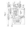
- FIG. 1 is a block diagram of a semiconductor memory device,. suchas aMOS type memory, to which the present invention may be applied.
- RAS denotes a row address strobe, CAS a column address strobe, A 0 to AN address input terminals, WE a write enable bar signal, D IN a data input, and D OUT a data output.
- reference numerals 1 and 2 designate clock generators
- reference numeral 3 designates address buffers
- reference numerals 4 and 5 designate a column decoder and a sense amplifier respectively
- reference numeral 6 designates a row decoder
- reference numeral 7 designates write clock generators
- reference numeral 8 designates a data-in buffer
- reference numeral 9 designates a data-out buffer
- reference numeral 10 designates a storage cell.
- the clock generator 1 generates a clock for operating the sense amplifier 5 and the row decoder 6, and the clock generator 2 generates a clock for operating the column decoder 4, the write clock generator 7, and the data-out buffer 9.
- the semiconductor memory device receives external control signals such as RAS, CAS, and WE, and the storage cell 10 is accessed and a read or write operation is carried out for the cell.
- an input circuit for the WE signal is provided with means for preventing the aforesaid malfunction in accordance with an embodiment of the present inventic ich an input circuit is included in the write clock generator 7 and receives the WE signal having a TTL level, that is, the high level thereof is 2.4 V or more and the low level thereof is 0.8 V or lower.
- this TTL level is converted to a MOS level signal, that is, having a high level that is the same as that of the high power source V CC (5 V), a low level that is the same as that of the low power source V SS (0), and the write clock generator 7 is operated by this converted output.
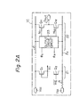
- FIG. 2A shows an output stage of the data output buffer and an input circuit of the WE signal, wherein 21 designates the input circuit and 22 designates the output stage. These circuits are connected to the high potential line l 1 of the power source and the low potential line 1 2 of the power source, the latter used as a reference potential line in a TTL logic level. system.
- the input circuit includes a depletion type MOS transistor Q 1 , in which a gate and a source are shortcircuited, and an enhancement type MOS transistor Q 2 connected to the transistor Q 1 in series.
- the input circuit is formed as an inverter having a series-connected point N 1 as an output terminal.
- the input WE signal enters a gate of the transistor Q2 , and when the input signal is H level and exceeds the threshold value of the transistor Q 2 , the transistor Q 2 turns ON and the output, that is, the level at the node N 1 becomes L level (V SS ).
- the transistor Q 2 turns OFF, and the output becomes H level (V CC ).
- This threshold level is set at an intermediate level between the TTL low and high levels, for example, at 1.6 V.
- the output stage 22 includes an output circuit having enhancement type MOS transistors Q 11 ' Q 12 connected in series, and a series-connected point used as an output terminal D out and an output drive circuit 23 thereof.
- the output drive circuit may be formed as shown in Fig. 2B.
- transistors Q13 to Q 18 are MOS transistors, and ⁇ S and ⁇ R are set and reset clocks for operating the drive circuit 23.
- Cell data DB and DB are supplied from the sense amplifier 5 (shown in Fig. 1) to the gate of the transistors Q 13 and Q 15 respectively.
- the transistors Q17 and Q18 for forming a latch and reset transistors Q 14 and Q 16 are provided so that the circuit is operated in a stabilized condition, therefore these transistors are not always necessary.
- the output drive circuit 23 receives the data read out by the clock signal ⁇ S and holds the data until the reset signal ⁇ R is received, and continuously drives the output circuit.
- the wiring of the power source line includes a resistance, shown by R in Fig. 2A.
- R in Fig. 2A When the transistor Q 12 at the output stage turns ON, the current flowing along the path mentioned above is comparatively large, and the phenomenon occurswhereby the voltage level at the wiring l 2 of V SS rises from V SS , that is, 0 V, due to the resistance mentioned above.
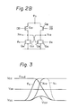
- V SS1 in Fig. 3 shows this rise in the level of the wiring of V SS .
- the WE signal may only be as high as slightly lower than 0.8 V for indicating L level (V IL ) and may/be as low as slightly higher than 2.4 V for indicating
- V IH H level
- the input transistor Q 2 can be turned on only when the difference between the input level at its gate and the internal V SS level applied to its source exceeds the threshold value of for example, 1.6 V. So , if the level at the wiring l 2 of V SS rises, the transistor Q 2 may not turn ON, even when the WE signal is at the H level, so that the problem occurs wherein the node N 1 (cannot) does not /generate an L output.
- the output N 1 of the input circuit is not L level, that is, at H level, the device is in the writing mode, and it is possible for the writing circuit in the device to operate and for the memory to carry out only the writing operation.
- the . writing circuit (not shown in the drawing) provides a latch function, so that, when the H level output is once generated, this is latched and an writing error (unwanted writing operation) may occur.
- the present invention can remove or mitigate this problem, and malfunction of the WE input circuit may be prevented line when the potential of the wiring /l 2 of V SS is caused to rise by the output current.
- FIG. 4 An embodiment of-the present invention will be explained by to Figs. 4 to 7.
- Q 1 and Q 2 are MOS transistors in an input circuit as shown in Fig. 2A
- the WE signal applied to a terminal pin of the memory chip is input to the gate of the transistor Q 2 .
- the output of the node N 1 is applied to a clock pulse generator circuit 31 in the writing system so that various clocks are generated and these are input to the writing circuit 32.
- RST designates a reset signal for stopping the generation of the clock in the circuit 31.
- a transistor Q 3 is connected in parallel to the transistor Q 2 in the input circuit 21, and a signal ⁇ D is applied to the gate of this transistor (e.g, enhancement /type MOS transistor )Q 3 .
- the signal ⁇ D may be the same as the input signal ⁇ S of the driving circuit 22, or , a signal which rises together with ⁇ S and falls thereafter (at a time when the rise of potential of the wiring l 2 of the power sourceline has finished).
- Two kinds of memory exist that is, one in which when the output stage transistor Q 12 or Q 11 is turned ON (the state which the output is held), the WE signal will not be received even if the WE signal is input (or varied), and only when both the output transistors Q 11 and Q 12 are turned OFF, the WE signal can be received; and the other in which even when the output stage transistor Q12 or Q11 is turned ON, the WE signal is received and the write operation becomes possible.
- the former may be supplied with signal 1, and the latter with 2 mentioned above.
- type Figure 5 shows a circuit for generating the signal ⁇ D of/2 mentioned above.
- Q 21 ⁇ Q31 are MOS transistors, and these transistors are connected between the power source lines V CC and V SS .
- ⁇ S and ⁇ R are a set signal and a reset signal supplied to the driving circuit 23 as mentioned above, and in the present circuit, they are supplied to the transistors Q 24 and Q 26 and the transistors Q 21 ' Q 27 ' and Q 28 .
- the transistors Q22 and Q25 turn ON, the potential at a node ⁇ 4 falls, and the signal ⁇ D also falls.
- the signal ⁇ D rises together with the rise of the signal ⁇ S' then falls so that a temporarily generated pulse is formed.
- the generating period of this pulse can be set by the capacity of the capacitor C.
- the pulse of the signal ⁇ D applied to transistor Q 3 in the input circuit causes transistor Q 3 to turn ON.
- the high level portion of the pulse is at V CC level and so is sufficient to turn on Q 3 even during the temporary level change V SS1 of the reference potential V SS .
- the high level portion of the pulse continues after the level change V SS1 has subsided, the duration of the pulse being determined by the capacitor C.
- the switching ON of transistor Q 3 ensures that the node N, generates an L output at the appropriate time, so that the writing mode is released and a writing error does not occur. Reading of data, under control of the signal ⁇ S , may then be performed correctly. A similar effect can be achieved by applying a signal ⁇ D of type 1 , the same as clock signal ⁇ S , to the transistor Q 3 .
- the WE signal may be received even when an output transistor Q 11 or Q 12 of the data output buffer is ON, it is preferable to maintain Q 2 in an ON state throughout the period in which the setting clock signal ⁇ S is high, so as to ensure that the writing mode is not set erroneously due to a change in the reference potential V SS or write enable bar signal WE. Accordingly, a signal of type 1 may be used.
- Figure 7 is similar to Fig.6, and shows the level change of the output D OUT' V SS' etc., and that the width of the signal ⁇ D is selected to be larger than the period of the level change V SS1 .
- a circuit in accordance with the present invention may be employed to overcome the effect of a fall in potential at the reference potential line occurring when the high level is output at the output stage.
Landscapes
- Engineering & Computer Science (AREA)
- Microelectronics & Electronic Packaging (AREA)
- Computer Hardware Design (AREA)
- Static Random-Access Memory (AREA)
- Dram (AREA)
- Logic Circuits (AREA)
Applications Claiming Priority (2)
| Application Number | Priority Date | Filing Date | Title |
|---|---|---|---|
| JP232733/84 | 1984-11-05 | ||
| JP59232733A JPS61110396A (ja) | 1984-11-05 | 1984-11-05 | 半導体記憶装置 |
Publications (3)
| Publication Number | Publication Date |
|---|---|
| EP0181177A2 true EP0181177A2 (fr) | 1986-05-14 |
| EP0181177A3 EP0181177A3 (en) | 1988-03-02 |
| EP0181177B1 EP0181177B1 (fr) | 1991-02-27 |
Family
ID=16943925
Family Applications (1)
| Application Number | Title | Priority Date | Filing Date |
|---|---|---|---|
| EP85307971A Expired - Lifetime EP0181177B1 (fr) | 1984-11-05 | 1985-11-04 | Dispositif de mémoire semi-conductrice |
Country Status (5)
| Country | Link |
|---|---|
| US (1) | US4970693A (fr) |
| EP (1) | EP0181177B1 (fr) |
| JP (1) | JPS61110396A (fr) |
| KR (1) | KR900007999B1 (fr) |
| DE (1) | DE3581888D1 (fr) |
Cited By (3)
| Publication number | Priority date | Publication date | Assignee | Title |
|---|---|---|---|---|
| EP0311102A3 (en) * | 1987-10-09 | 1989-09-27 | Kabushiki Kaisha Toshiba | Semiconductor ic including circuit for preventing erroneous operation caused by power source noise |
| EP0333206A3 (en) * | 1988-03-18 | 1990-01-31 | Kabushiki Kaisha Toshiba | Semiconductor integrated circuit |
| KR101124652B1 (ko) * | 2009-09-02 | 2012-03-20 | 와이즈팔 테크놀로지스 인코포레이티드 | 웨이퍼 레벨 모듈 제작 방법 |
Families Citing this family (10)
| Publication number | Priority date | Publication date | Assignee | Title |
|---|---|---|---|---|
| JP2777136B2 (ja) * | 1988-03-08 | 1998-07-16 | 株式会社東芝 | 半導体集積回路の誤動作防止回路 |
| US5206833A (en) * | 1988-09-12 | 1993-04-27 | Acer Incorporated | Pipelined dual port RAM |
| JPH0756749B2 (ja) * | 1989-09-29 | 1995-06-14 | 株式会社東芝 | 機能選択回路 |
| TW198135B (fr) * | 1990-11-20 | 1993-01-11 | Oki Electric Ind Co Ltd | |
| US5485430A (en) * | 1992-12-22 | 1996-01-16 | Sgs-Thomson Microelectronics, Inc. | Multiple clocked dynamic sense amplifier |
| JP2605576B2 (ja) * | 1993-04-02 | 1997-04-30 | 日本電気株式会社 | 同期型半導体メモリ |
| KR940026946A (ko) * | 1993-05-12 | 1994-12-10 | 김광호 | 데이타출력 확장방법과 이를 통한 신뢰성있는 유효데이타의 출력이 이루어지는 반도체집적회로 |
| JPH0715312A (ja) * | 1993-06-15 | 1995-01-17 | Fujitsu Ltd | 半導体記憶装置 |
| JP2697634B2 (ja) * | 1994-09-30 | 1998-01-14 | 日本電気株式会社 | 同期型半導体記憶装置 |
| US5550783A (en) * | 1995-04-19 | 1996-08-27 | Alliance Semiconductor Corporation | Phase shift correction circuit for monolithic random access memory |
Family Cites Families (6)
| Publication number | Priority date | Publication date | Assignee | Title |
|---|---|---|---|---|
| US4165541A (en) * | 1977-12-12 | 1979-08-21 | Fairchild Camera And Instrument Corporation | Serial-parallel-serial charge-coupled device memory having interlacing and ripple clocking of the parallel shift registers |
| US4337525A (en) * | 1979-04-17 | 1982-06-29 | Nippon Electric Co., Ltd. | Asynchronous circuit responsive to changes in logic level |
| JPS5835783A (ja) * | 1981-08-24 | 1983-03-02 | Fujitsu Ltd | 半導体メモリ |
| US4585955B1 (en) * | 1982-12-15 | 2000-11-21 | Tokyo Shibaura Electric Co | Internally regulated power voltage circuit for mis semiconductor integrated circuit |
| JPS6052112A (ja) * | 1983-08-31 | 1985-03-25 | Toshiba Corp | 論理回路 |
| US4638182A (en) * | 1984-07-11 | 1987-01-20 | Texas Instruments Incorporated | High-level CMOS driver circuit |
-
1984
- 1984-11-05 JP JP59232733A patent/JPS61110396A/ja active Granted
-
1985
- 1985-11-04 DE DE8585307971T patent/DE3581888D1/de not_active Expired - Lifetime
- 1985-11-04 EP EP85307971A patent/EP0181177B1/fr not_active Expired - Lifetime
- 1985-11-05 KR KR1019850008230A patent/KR900007999B1/ko not_active Expired
-
1990
- 1990-02-23 US US07/484,474 patent/US4970693A/en not_active Expired - Fee Related
Cited By (4)
| Publication number | Priority date | Publication date | Assignee | Title |
|---|---|---|---|---|
| EP0311102A3 (en) * | 1987-10-09 | 1989-09-27 | Kabushiki Kaisha Toshiba | Semiconductor ic including circuit for preventing erroneous operation caused by power source noise |
| US4896056A (en) * | 1987-10-09 | 1990-01-23 | Kabushiki Kaisha Toshiba | Semiconductor IC including circuit for preventing erroneous operation caused by power source noise |
| EP0333206A3 (en) * | 1988-03-18 | 1990-01-31 | Kabushiki Kaisha Toshiba | Semiconductor integrated circuit |
| KR101124652B1 (ko) * | 2009-09-02 | 2012-03-20 | 와이즈팔 테크놀로지스 인코포레이티드 | 웨이퍼 레벨 모듈 제작 방법 |
Also Published As
| Publication number | Publication date |
|---|---|
| JPS61110396A (ja) | 1986-05-28 |
| KR860004380A (ko) | 1986-06-20 |
| JPH0439158B2 (fr) | 1992-06-26 |
| EP0181177B1 (fr) | 1991-02-27 |
| EP0181177A3 (en) | 1988-03-02 |
| US4970693A (en) | 1990-11-13 |
| KR900007999B1 (ko) | 1990-10-23 |
| DE3581888D1 (de) | 1991-04-04 |
Similar Documents
| Publication | Publication Date | Title |
|---|---|---|
| US6564351B2 (en) | Circuit and method for testing an integrated circuit | |
| KR0135735B1 (ko) | 소음발생을 억제하는 개량된 출력 드라이버 회로 및 번인테스트를 위한 개량된 반도체 집적회로 장치 | |
| EP0624878B1 (fr) | Circuit intégré à semi-conducteurs | |
| US6125069A (en) | Semiconductor memory device with redundancy circuit having a reference resistance | |
| EP0217601A2 (fr) | Cellule de mémoire | |
| US4644501A (en) | Semiconductor memory device with charging circuit | |
| EP0301588A2 (fr) | Dispositif de mémoire à semi-conducteurs | |
| EP0181177B1 (fr) | Dispositif de mémoire semi-conductrice | |
| DE19503390C2 (de) | Datenausgabepuffer-Steuerschaltung | |
| US5333122A (en) | Electrically erasable and programmable non-volatile semiconductor memory device having word line voltage control circuit using internal voltage booster circuit | |
| KR930008577B1 (ko) | 반도체 메모리장치 | |
| KR940009079B1 (ko) | 노이즈로 인한 오동작을 방지하기 위한 반도체장치 | |
| US4791614A (en) | Semiconductor memory device having erroneous write operation preventing function | |
| US5517142A (en) | Output buffer with a reduced transient bouncing phenomenon | |
| US5307319A (en) | Initialization setting circuit and semiconductor memory device using the same | |
| KR940005697B1 (ko) | 용장 메모리 셀을 갖는 반도체 메모리 장치 | |
| EP0115140B1 (fr) | Circuit décodeur | |
| US5841718A (en) | Use of voltage equalization in signal-sensing circuits | |
| EP0329177A2 (fr) | Dispositif de mémoire à semi-conducteurs pouvant supprimer une faute d'opération due à un bruit d'alimentation | |
| US5402387A (en) | Semiconductor memory | |
| KR100399110B1 (ko) | 반도체장치 | |
| EP0148364B1 (fr) | Générateur de signal de référence temporelle | |
| JP3114237B2 (ja) | 半導体記憶装置 | |
| EP0333206B1 (fr) | Circuit intégré à semi-conducteurs | |
| EP0155787B1 (fr) | Dispositif de mémoire semi-conductrice |
Legal Events
| Date | Code | Title | Description |
|---|---|---|---|
| PUAI | Public reference made under article 153(3) epc to a published international application that has entered the european phase |
Free format text: ORIGINAL CODE: 0009012 |
|
| AK | Designated contracting states |
Kind code of ref document: A2 Designated state(s): DE FR GB |
|
| PUAL | Search report despatched |
Free format text: ORIGINAL CODE: 0009013 |
|
| AK | Designated contracting states |
Kind code of ref document: A3 Designated state(s): DE FR GB |
|
| 17P | Request for examination filed |
Effective date: 19880331 |
|
| 17Q | First examination report despatched |
Effective date: 19891201 |
|
| GRAA | (expected) grant |
Free format text: ORIGINAL CODE: 0009210 |
|
| AK | Designated contracting states |
Kind code of ref document: B1 Designated state(s): DE FR GB |
|
| ET | Fr: translation filed | ||
| REF | Corresponds to: |
Ref document number: 3581888 Country of ref document: DE Date of ref document: 19910404 |
|
| PLBE | No opposition filed within time limit |
Free format text: ORIGINAL CODE: 0009261 |
|
| STAA | Information on the status of an ep patent application or granted ep patent |
Free format text: STATUS: NO OPPOSITION FILED WITHIN TIME LIMIT |
|
| 26N | No opposition filed | ||
| PGFP | Annual fee paid to national office [announced via postgrant information from national office to epo] |
Ref country code: GB Payment date: 20011107 Year of fee payment: 17 |
|
| PGFP | Annual fee paid to national office [announced via postgrant information from national office to epo] |
Ref country code: FR Payment date: 20011113 Year of fee payment: 17 |
|
| PGFP | Annual fee paid to national office [announced via postgrant information from national office to epo] |
Ref country code: DE Payment date: 20011119 Year of fee payment: 17 |
|
| REG | Reference to a national code |
Ref country code: GB Ref legal event code: IF02 |
|
| PG25 | Lapsed in a contracting state [announced via postgrant information from national office to epo] |
Ref country code: GB Free format text: LAPSE BECAUSE OF NON-PAYMENT OF DUE FEES Effective date: 20021104 |
|
| PG25 | Lapsed in a contracting state [announced via postgrant information from national office to epo] |
Ref country code: DE Free format text: LAPSE BECAUSE OF NON-PAYMENT OF DUE FEES Effective date: 20030603 |
|
| GBPC | Gb: european patent ceased through non-payment of renewal fee | ||
| PG25 | Lapsed in a contracting state [announced via postgrant information from national office to epo] |
Ref country code: FR Free format text: LAPSE BECAUSE OF NON-PAYMENT OF DUE FEES Effective date: 20030731 |
|
| REG | Reference to a national code |
Ref country code: FR Ref legal event code: ST |