EP0181201A1 - Circuit d'attaque pour un transistor Darlington de puissance bipolaire - Google Patents
Circuit d'attaque pour un transistor Darlington de puissance bipolaire Download PDFInfo
- Publication number
- EP0181201A1 EP0181201A1 EP85308066A EP85308066A EP0181201A1 EP 0181201 A1 EP0181201 A1 EP 0181201A1 EP 85308066 A EP85308066 A EP 85308066A EP 85308066 A EP85308066 A EP 85308066A EP 0181201 A1 EP0181201 A1 EP 0181201A1
- Authority
- EP
- European Patent Office
- Prior art keywords
- transistor
- base
- diode
- emitter
- driver circuit
- Prior art date
- Legal status (The legal status is an assumption and is not a legal conclusion. Google has not performed a legal analysis and makes no representation as to the accuracy of the status listed.)
- Granted
Links
Images

Classifications
-
- H—ELECTRICITY
- H03—ELECTRONIC CIRCUITRY
- H03K—PULSE TECHNIQUE
- H03K17/00—Electronic switching or gating, i.e. not by contact-making and –breaking
- H03K17/04—Modifications for accelerating switching
- H03K17/041—Modifications for accelerating switching without feedback from the output circuit to the control circuit
- H03K17/0412—Modifications for accelerating switching without feedback from the output circuit to the control circuit by measures taken in the control circuit
- H03K17/04126—Modifications for accelerating switching without feedback from the output circuit to the control circuit by measures taken in the control circuit in bipolar transistor switches
-
- H—ELECTRICITY
- H03—ELECTRONIC CIRCUITRY
- H03K—PULSE TECHNIQUE
- H03K17/00—Electronic switching or gating, i.e. not by contact-making and –breaking
- H03K17/51—Electronic switching or gating, i.e. not by contact-making and –breaking characterised by the components used
- H03K17/56—Electronic switching or gating, i.e. not by contact-making and –breaking characterised by the components used by the use, as active elements, of semiconductor devices
- H03K17/60—Electronic switching or gating, i.e. not by contact-making and –breaking characterised by the components used by the use, as active elements, of semiconductor devices the devices being bipolar transistors
- H03K17/615—Electronic switching or gating, i.e. not by contact-making and –breaking characterised by the components used by the use, as active elements, of semiconductor devices the devices being bipolar transistors in a Darlington configuration
Definitions
- the present invention relates to a driver circuit for a bipolar Darlington power transistor, and more particularly to a driver circuit for switching a bipolar Darlington power transistor at a high speed and at a high frequency.
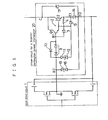
- Figure 2 shows a prior art base drive circuit for switching a bipolar Darlington power transistor at a high speed:
- the one end of the resistor 4 is connected to the anode of the diode 3 and the base of the transistor Q2 (the emitter of the transistor Ql).
- the cathode of the flywheel diode 5 is connected to the collector of the transistor Q2, and the anode of the flywheel diode 5 is connected to the emitter of the transistor Q2.
- a driver circuit for driving the bipolar Darlington power transistor 2 at a high speed and at a high frequency is constituted by a high speed switching diode 7 which applies a regular direction base current from the base drive circuit 1 to the base of the transistor Ql of the Darlington power transistor 2, a Baker clamp diode 6 for applying a regular direction extra base current to the collector of the transistor 2, and a high speed switching diode 8 for discharging the reverse direction base current from the transistor 2.
- the regular direction voltage drop of the Baker clamp diode 6 and that of the high speed switching diode 7 are preferably made equal to each other.
- This circuit is operated as follows:
- a reverse direction base current is given to the base of the transistor 2 through the diode 8.
- the transistor 2 is operated in an unsaturated or quasi-saturated region, and the storage time is almost zero, thereby to enable a high speed response.
- the reverse direction current which occurs in a case of inductive load is absorbed through the flywheel diode 5, or the resistor 4 and the diode 3.
- the Baker clamp diode 6 used in the circuit of Figure 2 it is required for the Baker clamp diode 6 used in the circuit of Figure 2 to have the same blocking voltage rating as that between the collector and base of the Darlington power transistor 2. Furthermore, it is required for the Baker clamp diode 6 and the high speed switching diode 7 to have equal regular voltage drops. However, when the blocking voltage rating of the power transistor 2 becomes large, it is quite difficult to obtain diodes which satisfies the both requirements.
- the present invention is directed to solve the problems pointed out above, and has for its object to provide a driver circuit for a bipolar Darlington power transistor capable of decreasing the turn-off loss and enabling the high frequency operation up to several tens KHz.
- Another object of the present invention is to provide a driver circuit for a bipolar Darlington power transistor capable of constituted by easily available elements.
- a driver circuit for a bipolar Darlington power transistor which comprises: a current clamping means which, provided between the base and emitter of said transistor, makes the base-emitter path of said transistor operate at a shallow saturated region; and a cutting off means which, provided at the side of said emitter, cuts-off said transistor in response to the signal given from the driving power source.
- a high speed recovery Schottky barrier diode 14 in reverse direction viewed from the emitter terminal E 2 so as to cut off the transistor 2 at a high speed.
- a flywheel diode 17 for absorbing the commutation current of the load current at the turn-off of the transistor 2.
- This circuit is operated as follows:
- a negative voltage having an absolute value larger than the sum of the break down voltage of the Zener diode 15 and the regular voltage drop of the high speed switching diode 16 is given to the base-emitter path of the transistor 2 from the base drive circuit 1.
- a reverse bias current flows from the emitter corresponding terminal E 2 of the base drive circuit 1 to the base terminal B 2 of the base drive circuit 1 through the diode 16 and the Zener diode 15.
- a reverse bias voltage having the value of the sum of the break down voltage of the Zener diode 15 and the regular voltage drop of the diode 16 (hereinafter referred to as a voltage "V R ”) is applied to between the anode and cathode of the high speed recovery Schottky barrier diode 14.
- V R a voltage having the value of the sum of the break down voltage of the Zener diode 15 and the regular voltage drop of the diode 16
- a Zener diode for clamping the base-emitter path of the bipolar power transistor in Darlington connection, a Schottky barrier diode for cutting off the emitter circuit of the bipolar power transistor at a high speed, and a high speed switching diode for discharging the storage charges. Therefore, it is possible to ignore the influences by the storage charges, and furthermore to reduce the turn-off time of the bipolar transistor to a great extent by the Schottky barrier diode, whereby a switching cirucit capable of operating at a high speed and a high frequency is obtained.
Landscapes
- Electronic Switches (AREA)
- Bipolar Integrated Circuits (AREA)
Applications Claiming Priority (2)
| Application Number | Priority Date | Filing Date | Title |
|---|---|---|---|
| JP233719/84 | 1984-11-06 | ||
| JP59233719A JPS61112421A (ja) | 1984-11-06 | 1984-11-06 | バイポ−ラ・ダ−リントン・パワ−トランジスタの駆動回路 |
Publications (2)
| Publication Number | Publication Date |
|---|---|
| EP0181201A1 true EP0181201A1 (fr) | 1986-05-14 |
| EP0181201B1 EP0181201B1 (fr) | 1989-05-17 |
Family
ID=16959486
Family Applications (1)
| Application Number | Title | Priority Date | Filing Date |
|---|---|---|---|
| EP85308066A Expired EP0181201B1 (fr) | 1984-11-06 | 1985-11-06 | Circuit d'attaque pour un transistor Darlington de puissance bipolaire |
Country Status (4)
| Country | Link |
|---|---|
| US (1) | US4777386A (fr) |
| EP (1) | EP0181201B1 (fr) |
| JP (1) | JPS61112421A (fr) |
| DE (1) | DE3570339D1 (fr) |
Cited By (3)
| Publication number | Priority date | Publication date | Assignee | Title |
|---|---|---|---|---|
| GB2251348A (en) * | 1990-07-25 | 1992-07-01 | Power Trends Inc | Programmed level gate driver for switching power supply |
| DE102013102097A1 (de) * | 2013-03-04 | 2014-09-04 | Phoenix Contact Gmbh & Co. Kg | Schaltungsanordnung |
| WO2021028648A1 (fr) * | 2019-08-12 | 2021-02-18 | Search For The Next Ltd | Circuit et dispositif comprenant un transistor et une diode |
Families Citing this family (10)
| Publication number | Priority date | Publication date | Assignee | Title |
|---|---|---|---|---|
| US4823070A (en) | 1986-11-18 | 1989-04-18 | Linear Technology Corporation | Switching voltage regulator circuit |
| DE4133764C1 (fr) * | 1991-10-11 | 1993-02-18 | Texas Instruments Deutschland Gmbh, 8050 Freising, De | |
| US5291069A (en) * | 1992-12-15 | 1994-03-01 | International Business Machines Corporation | Bipolar H write driver |
| US6861909B1 (en) | 2002-06-17 | 2005-03-01 | Sirenza Microdevices, Inc. | High voltage-wide band amplifier |
| EP1443649B1 (fr) * | 2003-01-31 | 2008-08-13 | STMicroelectronics S.r.l. | Configuration de commutation par l'émetteur et structure intégrée correspondante |
| US6806778B1 (en) | 2003-02-18 | 2004-10-19 | Sirenza Microdevices, Inc. | Darlington cascode |
| US6897707B2 (en) * | 2003-06-11 | 2005-05-24 | Northrop Grumman Corporation | Isolated FET drive utilizing Zener diode based systems, methods and apparatus |
| WO2015070344A1 (fr) * | 2013-11-14 | 2015-05-21 | Tm4 Inc. | Circuit de compensation, cellule de commutation et convertisseur de puissance commandant l'activation et la désactivation d'un commutateur électronique de puissance |
| US10562123B2 (en) * | 2015-06-18 | 2020-02-18 | Illinois Tool Works Inc. | Welding system with arc control |
| CN108141129B (zh) * | 2015-09-14 | 2020-07-14 | Tm4股份有限公司 | 配置为限制开关过电压的电力转换器 |
Family Cites Families (6)
| Publication number | Priority date | Publication date | Assignee | Title |
|---|---|---|---|---|
| US2892952A (en) * | 1957-06-27 | 1959-06-30 | Eugene S Mcvey | Ramp function transistor circuit |
| US3751680A (en) * | 1972-03-02 | 1973-08-07 | Signetics Corp | Double-clamped schottky transistor logic gate circuit |
| JPS50145840A (fr) * | 1974-05-11 | 1975-11-22 | ||
| US4112314A (en) * | 1977-08-26 | 1978-09-05 | International Business Machines Corporation | Logical current switch |
| FR2458904A1 (fr) * | 1979-06-12 | 1981-01-02 | Thomson Csf | Circuit integre monolithique equivalent a un transistor associe a trois diodes anti-saturation |
| US4400635A (en) * | 1981-01-21 | 1983-08-23 | Rca Corporation | Wide temperature range switching circuit |
-
1984
- 1984-11-06 JP JP59233719A patent/JPS61112421A/ja active Pending
-
1985
- 1985-11-06 EP EP85308066A patent/EP0181201B1/fr not_active Expired
- 1985-11-06 DE DE8585308066T patent/DE3570339D1/de not_active Expired
-
1987
- 1987-10-19 US US07/110,588 patent/US4777386A/en not_active Expired - Lifetime
Non-Patent Citations (2)
| Title |
|---|
| ELECTRONIQUE APPLICATIONS, no. 31, August-September 1983, pages 35-44, Evry, FR; K.K. RISCHMULLER "Darlington, Bipmos, Cascode: caractéristiques et critères d'emploi" * |
| ELECTRONIQUE INDUSTRIELLE, no. 9, 1st February 1981, pages 21-23, Paris, FR; P. ALOISI "Darlingtons pour triphasé 380-420 V" * |
Cited By (7)
| Publication number | Priority date | Publication date | Assignee | Title |
|---|---|---|---|---|
| GB2251348A (en) * | 1990-07-25 | 1992-07-01 | Power Trends Inc | Programmed level gate driver for switching power supply |
| GB2251348B (en) * | 1990-07-25 | 1995-01-11 | Power Trends Inc | Programmed level gate drive for a miniaturised switching power supply |
| DE102013102097A1 (de) * | 2013-03-04 | 2014-09-04 | Phoenix Contact Gmbh & Co. Kg | Schaltungsanordnung |
| DE102013102097B4 (de) * | 2013-03-04 | 2014-12-04 | Phoenix Contact Gmbh & Co. Kg | Schaltungsanordnung |
| WO2021028648A1 (fr) * | 2019-08-12 | 2021-02-18 | Search For The Next Ltd | Circuit et dispositif comprenant un transistor et une diode |
| EP4401315A2 (fr) * | 2019-08-12 | 2024-07-17 | Search For The Next Ltd | Circuit et dispositif comprenant un transistor et une diode |
| TWI875797B (zh) * | 2019-08-12 | 2025-03-11 | 英商瑟其福耐斯特有限公司 | 包括電晶體和二極體的電路和裝置 |
Also Published As
| Publication number | Publication date |
|---|---|
| JPS61112421A (ja) | 1986-05-30 |
| DE3570339D1 (en) | 1989-06-22 |
| US4777386A (en) | 1988-10-11 |
| EP0181201B1 (fr) | 1989-05-17 |
Similar Documents
| Publication | Publication Date | Title |
|---|---|---|
| US5281862A (en) | Power MOSFET driver with cross-conduction current reduction | |
| US4500801A (en) | Self-powered nonregenerative fast gate turn-off FET | |
| US4360744A (en) | Semiconductor switching circuits | |
| US4500802A (en) | Three terminal bidirectional source to source FET circuit | |
| EP0181201A1 (fr) | Circuit d'attaque pour un transistor Darlington de puissance bipolaire | |
| EP0181148B1 (fr) | Dispositif à semi-conducteur | |
| US4414479A (en) | Low dissipation snubber for switching power transistors | |
| JP2777307B2 (ja) | 短絡保護回路 | |
| US4322785A (en) | Transistor switching circuit | |
| EP0379320A1 (fr) | Circuit de couplage optique | |
| US4246501A (en) | Gated back-clamped transistor switching circuit | |
| US4603268A (en) | Totem pole output circuit with reduced current spikes | |
| KR910010869A (ko) | 전력 fet용 적응 게이트 방전 회로 | |
| GB1599262A (en) | Transistor switching circuit | |
| US4916378A (en) | Inductive load discharge current recirculation circuit with selectable "fast" and "low" modes | |
| EP0402663A2 (fr) | Circuit de commande | |
| US5361009A (en) | Thyristor controller | |
| US4746814A (en) | Semiconductor device for conducting primary current upon receipt of a control signal | |
| US3927332A (en) | Drive circuit for controlling conduction of a semiconductor device | |
| US4698519A (en) | Monolithically integratable high-efficiency control circuit for switching transistors | |
| US4602209A (en) | Switch-off circuits for transistors and gate turn-off thyristors | |
| EP0177148A2 (fr) | Alimentation de puissance comportant des éléments "MOSFET" | |
| EP0427084A2 (fr) | Circuit cascode à excursion maximale pour une pompe de charge bipolaire | |
| SU1051717A1 (ru) | Полупроводниковый ключ | |
| GB2050739A (en) | Transistor switching circuit |
Legal Events
| Date | Code | Title | Description |
|---|---|---|---|
| PUAI | Public reference made under article 153(3) epc to a published international application that has entered the european phase |
Free format text: ORIGINAL CODE: 0009012 |
|
| AK | Designated contracting states |
Kind code of ref document: A1 Designated state(s): DE FR GB |
|
| 17P | Request for examination filed |
Effective date: 19860728 |
|
| 17Q | First examination report despatched |
Effective date: 19871103 |
|
| GRAA | (expected) grant |
Free format text: ORIGINAL CODE: 0009210 |
|
| AK | Designated contracting states |
Kind code of ref document: B1 Designated state(s): DE FR GB |
|
| REF | Corresponds to: |
Ref document number: 3570339 Country of ref document: DE Date of ref document: 19890622 |
|
| ET | Fr: translation filed | ||
| PLBE | No opposition filed within time limit |
Free format text: ORIGINAL CODE: 0009261 |
|
| STAA | Information on the status of an ep patent application or granted ep patent |
Free format text: STATUS: NO OPPOSITION FILED WITHIN TIME LIMIT |
|
| 26N | No opposition filed | ||
| PGFP | Annual fee paid to national office [announced via postgrant information from national office to epo] |
Ref country code: GB Payment date: 19931027 Year of fee payment: 9 |
|
| PGFP | Annual fee paid to national office [announced via postgrant information from national office to epo] |
Ref country code: FR Payment date: 19931110 Year of fee payment: 9 Ref country code: DE Payment date: 19931110 Year of fee payment: 9 |
|
| PG25 | Lapsed in a contracting state [announced via postgrant information from national office to epo] |
Ref country code: GB Effective date: 19941106 |
|
| GBPC | Gb: european patent ceased through non-payment of renewal fee |
Effective date: 19941106 |
|
| PG25 | Lapsed in a contracting state [announced via postgrant information from national office to epo] |
Ref country code: FR Effective date: 19950731 |
|
| PG25 | Lapsed in a contracting state [announced via postgrant information from national office to epo] |
Ref country code: DE Effective date: 19950801 |
|
| REG | Reference to a national code |
Ref country code: FR Ref legal event code: ST |