EP0181206A2 - Halbleitervorrichtungen - Google Patents
Halbleitervorrichtungen Download PDFInfo
- Publication number
- EP0181206A2 EP0181206A2 EP85308078A EP85308078A EP0181206A2 EP 0181206 A2 EP0181206 A2 EP 0181206A2 EP 85308078 A EP85308078 A EP 85308078A EP 85308078 A EP85308078 A EP 85308078A EP 0181206 A2 EP0181206 A2 EP 0181206A2
- Authority
- EP
- European Patent Office
- Prior art keywords
- integrated circuit
- semiconductor
- semiconductor integrated
- circuit according
- semiconductor device
- Prior art date
- Legal status (The legal status is an assumption and is not a legal conclusion. Google has not performed a legal analysis and makes no representation as to the accuracy of the status listed.)
- Withdrawn
Links
Images

Classifications
-
- H—ELECTRICITY
- H03—ELECTRONIC CIRCUITRY
- H03F—AMPLIFIERS
- H03F1/00—Details of amplifiers with only discharge tubes, only semiconductor devices or only unspecified devices as amplifying elements
- H03F1/30—Modifications of amplifiers to reduce influence of variations of temperature or supply voltage or other physical parameters
- H03F1/301—Modifications of amplifiers to reduce influence of variations of temperature or supply voltage or other physical parameters in MOSFET amplifiers
-
- G—PHYSICS
- G01—MEASURING; TESTING
- G01N—INVESTIGATING OR ANALYSING MATERIALS BY DETERMINING THEIR CHEMICAL OR PHYSICAL PROPERTIES
- G01N27/00—Investigating or analysing materials by the use of electric, electrochemical, or magnetic means
- G01N27/26—Investigating or analysing materials by the use of electric, electrochemical, or magnetic means by investigating electrochemical variables; by using electrolysis or electrophoresis
- G01N27/403—Cells and electrode assemblies
- G01N27/414—Ion-sensitive or chemical field-effect transistors, i.e. ISFETS or CHEMFETS
- G01N27/4148—Integrated circuits therefor, e.g. fabricated by CMOS processing
-
- Y—GENERAL TAGGING OF NEW TECHNOLOGICAL DEVELOPMENTS; GENERAL TAGGING OF CROSS-SECTIONAL TECHNOLOGIES SPANNING OVER SEVERAL SECTIONS OF THE IPC; TECHNICAL SUBJECTS COVERED BY FORMER USPC CROSS-REFERENCE ART COLLECTIONS [XRACs] AND DIGESTS
- Y10—TECHNICAL SUBJECTS COVERED BY FORMER USPC
- Y10S—TECHNICAL SUBJECTS COVERED BY FORMER USPC CROSS-REFERENCE ART COLLECTIONS [XRACs] AND DIGESTS
- Y10S435/00—Chemistry: molecular biology and microbiology
- Y10S435/817—Enzyme or microbe electrode
Definitions
- This invention relates to semiconductor devices and, in particular, to semiconductor devices capable of the detection and measurement of physico-chemical properties.
- "'Chemical properties" as used herein shall be understood to include ion activity and concentration, presence and concentration of enzymes, substrates, antibodies, antigens, hormones and reproducible gases and the pressure, concentration and activity of chemical and biochemical systems including the constituents of enzymatic systems such as serum enzymes, glucose, lactates, pyrurates, creatinine, urea and the constituents of the immunilogical system.
- a semiconductor integrated circuit including a first semiconductor device sensitive to a physico-chemical property of an ambient to which it is exposed and capable of producing an output signal dependent on said physico-chemical property, a second semiconductor device insensitive to said physico-chemical property but having a geometry and physical structure substantially identical with that of said first semiconductor device and being coupled thermally to said first semiconductor device together with differential amplifer means the input of which is coupled to the outputs of said first and second semiconductor devices and the output of which is coupled to the input of one of said first and second semiconductors.
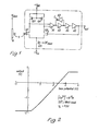
- FIG. 1 A practical embodiment of a device in accordance with the invention in the form of an operational transducer is illustrated in Figure 1.
- a chemical-sensing field-effect transistor Q1 configured to be non-inverting and exposed to solution S and an insulated-gate field-effect transistor Q2 configured to be inverting were connected to a differential amplifier A1 feeding a cascode amplifier A2 with a source follower loop A3,C.
- the high output impedance of the cascode was matched by a source follower stage A4 to the low imput impedance of an output amplifier A5. Feedback from the output stage to the control electrode of the insulated-gate FET Q2 provided compensation for thermal effects, which are rejected as a common-made signal.
- the electrochemical potential of the ambient solution phase to which the transducer is exposed is maintained at a constant value with respect to that of the semiconductor substrate of the operational transducer by means of a reference electrode R connected to a bias voltage source V bias .
- Electron-beam lithography was used to write the designs onto the mask set used for processing.
- Devices were fabricated on 75 mm diameter, p-type, 14-20 ohm cm, (100) orientation silicon wafers, using a modified n-channel MNOS process.
- Half of the wafer batch were given light, n-type channel ion-implants (depletion mode), and the remainder were lightly implanted with p-type impurities (enhancement-mode); resultant threshold voltages (V T ) were approximately -1.0 V and +1.0 V respectively.
- a p-type channel-stopper implant was incorporated, and a 6,000A thick film of polyimide was used for a final, protective overlay, with only the bonding pads and ChemFET gate area remaining exposed.
- the die size was 2.03 x 2.43 mm.
- the operation transducer chip includes a 72 x 484 um aperture in the polyimide overlay for the ChemFET gate; the channel dimensions were 12 x 432 pm, and the gate area was surrounded by three concentric octagonal frames (600, 700 and 800 um diameter), for targetting ink dots which was used during polyimide/photopolymer encapsulation.
- the operational transducers were mounted and wire bonded onto the tips of 9 mm x 94 mm printed-circuit board substrates, so as to form dip-type sensors for electrochemical evaluation, and were selectively encapsulated using either H-54 epoxy resin, or a polyimide/photoresist composite, leaving only the Si 3 N 4 surface of the active gate region exposed.
- the silicon nitride gate dielectric surface of the transducer is intrinsically pH-responsive (3,44).
- Potassium-responsive transducers were made by casting, from solution, an ionophore-doped, polymeric film (by weight: 1% valinomycin; 66X bis(2-ethylhexyl) adipate; 33% poly(vinylchloride)), over the exposed gate, using cyclohexanone as the solvent. A single drop of the doped-polymer solution was applied to each gate, and then the solvent was removed by vacuum desiccation for 12 hours at ambient temperature. The resultant films were approximately 50 ⁇ m thick.
- the transfer characteristics of a typical transducer made by the above process are shown in Figure 2.
- the input offset voltage lies typically in the range -30 - +120 mV, however a relatively large input offset voltage is invariably observed in the chemoresponsive transducer characteristics, and is usually in the range +1 - +2.5 V. This is due to the difference in threshold voltages between the metallised-gate/Si 3 N 4 -gate differential pair, which is caused by the electrochemical differences in gate contact mechanism, and is largely unimportant (viz. the matching is not affected). There is only a very slight optical sensitivity; a change from ambiment illumination to darkness results in a -3 mV change in output signal.
- the electrochemical response of a pH-sensitive transducer i.e. having a Si 3 N 4 gate
- the response is linear, but somewhat sub-Nernstian (46.2 mV/decade), however the latter is a common feature of field-effect sensors having Si 3 N 4 as the electroactive gate material.
- Devices with Si 3 N 4 gates have been found to operate satisfactorily throughout the range pH 1 to pH 14.
- the rate of response to a step change in pH was too rapid to sensibly quantify; being several hundreds ms, at most.
- the electrochemical characteristics of a K transducer are shown in Figure 4.
- the response is virtually Nerstian over the K + concentration range 10 1 - 10 mol 1 -1 , having a slope of 57.8 mV/decade; the response time is, again, too rapid to quantify ( ⁇ 500 ms).
- the H and K transducers are not subject to any hysteresis or spurious, small voltage offsets caused by dipping between solutions of disconnecting the reference electrode, as discrete ChemFET devices are prone to be when operated in constant current mode. A stable output potential was established almost instantaneously when the transducer is placed in solution.
- the thermal characteristics of a transducer having an aluminium gate biased to 0V are shown in Figure 6.
- the output signal was recorded at ambient temperature (22°C) for 6 minutes, then the transducer was placed in an oven, thermostatted at 72°C; 4 minutes later, the output potential was again stable after a 1.2 mV shift (viz. the input offset voltage thermal coefficient is approximately 24 ⁇ V°C -1 ), then 3 minutes later the transducer was returned to ambient temperature.
- a very small background signal drift ( ⁇ 1.5 mV hr ) was apparent, and can be attributed to burn-in effects.
- transducers can be used to deposit both inorganic and organic gate materials, including metal oxides and halides, ionophore-doped polymeric films and others, where the resultant film would be too fragile or insufficiently conductive for use in a conventional ion-selective electrode.
- film techniques such as vacuum evaporation and sputtering, chemical vapour deposition, spin-coating, etc.
- inorganic and organic gate materials including metal oxides and halides, ionophore-doped polymeric films and others, where the resultant film would be too fragile or insufficiently conductive for use in a conventional ion-selective electrode.
- the operational transducer concept is not limited to ion-selective sensor applications, and is compatible with any type of discrete field-effect chemical sensor, including enhancement and depletion-mode FETs, offset gate FETs, junction FETs, gapped-gate devices, suspended mesh variants and devices with electrostatic gate protection. Neither are the devices nor is it restricted to implementation using an NMOS process, the use of CMOS technology would permit a simpler design having fewer transistors. Other worthwhile developments would be the inclusion of electrostatic protection and on-chip temperature measurement, and the fabrication of a multi-function operational transducer array for the simultaneous measurement of several different species, such as H K and Na .
Landscapes
- Engineering & Computer Science (AREA)
- Life Sciences & Earth Sciences (AREA)
- Chemical & Material Sciences (AREA)
- Microelectronics & Electronic Packaging (AREA)
- Health & Medical Sciences (AREA)
- Physics & Mathematics (AREA)
- Biochemistry (AREA)
- Computer Hardware Design (AREA)
- Chemical Kinetics & Catalysis (AREA)
- Electrochemistry (AREA)
- Power Engineering (AREA)
- Analytical Chemistry (AREA)
- Molecular Biology (AREA)
- General Health & Medical Sciences (AREA)
- General Physics & Mathematics (AREA)
- Immunology (AREA)
- Pathology (AREA)
- Investigating Or Analyzing Materials By The Use Of Electric Means (AREA)
- Investigating Or Analyzing Materials By The Use Of Fluid Adsorption Or Reactions (AREA)
- Junction Field-Effect Transistors (AREA)
- Amplifiers (AREA)
Applications Claiming Priority (2)
| Application Number | Priority Date | Filing Date | Title |
|---|---|---|---|
| GB8428138 | 1984-11-07 | ||
| GB848428138A GB8428138D0 (en) | 1984-11-07 | 1984-11-07 | Semiconductor devices |
Publications (2)
| Publication Number | Publication Date |
|---|---|
| EP0181206A2 true EP0181206A2 (de) | 1986-05-14 |
| EP0181206A3 EP0181206A3 (de) | 1988-01-20 |
Family
ID=10569381
Family Applications (1)
| Application Number | Title | Priority Date | Filing Date |
|---|---|---|---|
| EP85308078A Withdrawn EP0181206A3 (de) | 1984-11-07 | 1985-11-06 | Halbleitervorrichtungen |
Country Status (4)
| Country | Link |
|---|---|
| US (1) | US4657658A (de) |
| EP (1) | EP0181206A3 (de) |
| JP (1) | JPS61118652A (de) |
| GB (2) | GB8428138D0 (de) |
Cited By (3)
| Publication number | Priority date | Publication date | Assignee | Title |
|---|---|---|---|---|
| EP0300651A3 (en) * | 1987-07-10 | 1989-12-20 | Molecular Devices Corporation | Photoresponsive electrode for determination of redox potential |
| WO1990001694A1 (de) * | 1988-08-11 | 1990-02-22 | Norbert Hampp | Chemosensitiver wandler |
| WO1998041853A1 (en) * | 1997-03-14 | 1998-09-24 | Osmetech Plc | Gas sensor |
Families Citing this family (24)
| Publication number | Priority date | Publication date | Assignee | Title |
|---|---|---|---|---|
| US4879517A (en) * | 1988-07-25 | 1989-11-07 | General Signal Corporation | Temperature compensation for potentiometrically operated ISFETS |
| US4974592A (en) * | 1988-11-14 | 1990-12-04 | American Sensor Systems Corporation | Continuous on-line blood monitoring system |
| KR930002824B1 (ko) * | 1990-08-21 | 1993-04-10 | 손병기 | 감이온 전계효과 트랜지스터를 이용한 바이오 센서용 측정회로 |
| US6320429B1 (en) | 1991-06-28 | 2001-11-20 | Fuji Electric Co., Ltd. | Integrated circuit having a comparator circuit including at least one differential amplifier |
| CA2066929C (en) * | 1991-08-09 | 1996-10-01 | Katsuji Kimura | Temperature sensor circuit and constant-current circuit |
| KR940010562B1 (ko) * | 1991-09-06 | 1994-10-24 | 손병기 | Ta_2O_5수소이온 감지막을 갖는 감이온 전계효과 트랜지스터의 제조방법 |
| DE4228609C1 (de) * | 1992-08-28 | 1994-01-20 | Fraunhofer Ges Forschung | Vorrichtung zur Messung von Ionenkonzentrationen in Lösungen |
| US5546041A (en) * | 1993-08-05 | 1996-08-13 | Massachusetts Institute Of Technology | Feedback sensor circuit |
| US5414284A (en) * | 1994-01-19 | 1995-05-09 | Baxter; Ronald D. | ESD Protection of ISFET sensors |
| US5833824A (en) * | 1996-11-15 | 1998-11-10 | Rosemount Analytical Inc. | Dorsal substrate guarded ISFET sensor |
| US6137341A (en) * | 1998-09-03 | 2000-10-24 | National Semiconductor Corporation | Temperature sensor to run from power supply, 0.9 to 12 volts |
| US6218208B1 (en) | 1999-07-02 | 2001-04-17 | National Science Council | Fabrication of a multi-structure ion sensitive field effect transistor with a pH sensing layer of a tin oxide thin film |
| ES2165809B1 (es) * | 2000-06-21 | 2003-02-16 | Univ Valencia Estudi General | Sistema de medida basado en sensores isfets/memfets que permite variar el punto de operacion del sensor y determinar la concentracion de iones en un medio liquido. |
| TW468233B (en) | 2000-09-16 | 2001-12-11 | Univ Nat Yunlin Sci & Tech | Apparatus and measurement method of hysteresis and time shift for ISFET containing amorphous silicon hydride sensing membrane |
| JP3883512B2 (ja) * | 2001-04-23 | 2007-02-21 | 三星電子株式会社 | 微細流路の側壁に形成されたmosfetよりなる物質検出用チップ、これを含む物質検出装置、及び物質検出装置を利用した物質検出方法 |
| US20070159325A1 (en) * | 2004-11-16 | 2007-07-12 | Biowam Llc | Methodology and Apparatus for the Detection of Biological Substances |
| US8129978B2 (en) | 2006-07-13 | 2012-03-06 | National University Corporation Nagoya University | Material detector |
| TW200815750A (en) * | 2006-09-19 | 2008-04-01 | Univ Nat Yunlin Sci & Tech | System of measuring pH values of solutions and method for reducing time-drift effects of sensors thereof |
| US20080108164A1 (en) * | 2006-11-06 | 2008-05-08 | Oleynik Vladislav A | Sensor System and Method |
| US20110024305A1 (en) * | 2009-07-29 | 2011-02-03 | Ervin Matthew H | Differential Amplifier Sensor Architecture for Increased Sensing Selectivity |
| US9029132B2 (en) | 2009-08-06 | 2015-05-12 | International Business Machines Corporation | Sensor for biomolecules |
| US8052931B2 (en) * | 2010-01-04 | 2011-11-08 | International Business Machines Corporation | Ultra low-power CMOS based bio-sensor circuit |
| US9068935B2 (en) | 2010-04-08 | 2015-06-30 | International Business Machines Corporation | Dual FET sensor for sensing biomolecules and charged ions in an electrolyte |
| JP5494395B2 (ja) * | 2010-09-28 | 2014-05-14 | 大日本印刷株式会社 | バイオセンサ |
Family Cites Families (3)
| Publication number | Priority date | Publication date | Assignee | Title |
|---|---|---|---|---|
| US3703650A (en) * | 1971-09-16 | 1972-11-21 | Signetics Corp | Integrated circuit with temperature compensation for a field effect transistor |
| GB2077439B (en) * | 1980-04-28 | 1984-03-28 | Kuraray Co | Compensating temperature-dependent characteristic changes in ion-sensitive fet transducers |
| FR2516656A1 (fr) * | 1981-11-18 | 1983-05-20 | Commissariat Energie Atomique | Dispositif de mesure de la concentration d'une espece chimique ionique et application de ce dispositif a la mesure du ph d'une solution |
-
1984
- 1984-11-07 GB GB848428138A patent/GB8428138D0/en active Pending
-
1985
- 1985-11-06 EP EP85308078A patent/EP0181206A3/de not_active Withdrawn
- 1985-11-06 GB GB08527306A patent/GB2166904B/en not_active Expired
- 1985-11-07 JP JP60249936A patent/JPS61118652A/ja active Pending
- 1985-11-07 US US06/795,835 patent/US4657658A/en not_active Expired - Fee Related
Cited By (3)
| Publication number | Priority date | Publication date | Assignee | Title |
|---|---|---|---|---|
| EP0300651A3 (en) * | 1987-07-10 | 1989-12-20 | Molecular Devices Corporation | Photoresponsive electrode for determination of redox potential |
| WO1990001694A1 (de) * | 1988-08-11 | 1990-02-22 | Norbert Hampp | Chemosensitiver wandler |
| WO1998041853A1 (en) * | 1997-03-14 | 1998-09-24 | Osmetech Plc | Gas sensor |
Also Published As
| Publication number | Publication date |
|---|---|
| US4657658A (en) | 1987-04-14 |
| GB8428138D0 (en) | 1984-12-12 |
| GB2166904A (en) | 1986-05-14 |
| EP0181206A3 (de) | 1988-01-20 |
| GB2166904B (en) | 1987-12-31 |
| GB8527306D0 (en) | 1985-12-11 |
| JPS61118652A (ja) | 1986-06-05 |
Similar Documents
| Publication | Publication Date | Title |
|---|---|---|
| US4657658A (en) | Semiconductor devices | |
| Chin et al. | A novel SnO2/Al discrete gate ISFET pH sensor with CMOS standard process | |
| US5155061A (en) | Method for fabricating a silicon pressure sensor incorporating silicon-on-insulator structures | |
| US4771639A (en) | Semiconductor pressure sensor | |
| TW586228B (en) | Method for fabricating a titanium nitride sensing membrane on an EGFET | |
| EP1774306B1 (de) | Signalprozessierungsschaltkreis mit ionensensitivem feldeffekttransistor sowie verfahren zur überwachung einer eigenschaft einer flüssigkeit | |
| Lauks et al. | The extended gate chemically sensitive field effect transistor as multi-species microprobe | |
| EP2568282B1 (de) | Ionempfindlicher Detektor | |
| Chin et al. | Titanium nitride membrane application to extended gate field effect transistor pH sensor using VLSI technology | |
| EP3043173B1 (de) | Feuchtigkeitssensor | |
| US7592854B2 (en) | Temperature sensing circuit | |
| Ishihara et al. | CMOS integrated silicon pressure sensor | |
| US20040256685A1 (en) | Biosensor, method of manufacturing sensing unit thereof, and measuring system | |
| US6387724B1 (en) | Method of fabricating silicon-on-insulator sensor having silicon oxide sensing surface | |
| US4875011A (en) | Magnetic sensor using integrated silicon Hall effect elements formed on the (100) plane of a silicon substrate | |
| US6897081B2 (en) | Method for fabricating a monolithic chip including pH, temperature and photo-intensity multi-sensors and a readout circuit | |
| US7019343B2 (en) | SnO2 ISFET device, manufacturing method, and methods and apparatus for use thereof | |
| EP0118605B1 (de) | Rückkopplungskreis für halbleitende aktive Fühlerelemente | |
| Poghossian | Method of fabrication of ISFET-based biosensors on an Si–SiO2–Si structure | |
| US6683358B1 (en) | Silicon integrated accelerometer | |
| US6867059B2 (en) | A-C:H ISFET device manufacturing method, and testing methods and apparatus thereof | |
| JPH0972805A (ja) | 半導体センサ | |
| Khanna et al. | Design and development of a novel high-transconductance pH-ISFET (ion-sensitive field-effect transistor)-based glucose biosensor | |
| Chen et al. | The fabrication and characterisation of ion-sensitive field-effect transistors with a silicon dioxide gate | |
| JPH08204251A (ja) | GaAsホール素子 |
Legal Events
| Date | Code | Title | Description |
|---|---|---|---|
| PUAI | Public reference made under article 153(3) epc to a published international application that has entered the european phase |
Free format text: ORIGINAL CODE: 0009012 |
|
| AK | Designated contracting states |
Kind code of ref document: A2 Designated state(s): DE FR NL |
|
| RAP1 | Party data changed (applicant data changed or rights of an application transferred) |
Owner name: NATIONAL RESEARCH DEVELOPMENT CORPORATION |
|
| RIN1 | Information on inventor provided before grant (corrected) |
Inventor name: PIBBALD, ALASTAIR |
|
| 17P | Request for examination filed |
Effective date: 19861014 |
|
| RIN1 | Information on inventor provided before grant (corrected) |
Inventor name: SIBBALD, ALASTAIR |
|
| PUAL | Search report despatched |
Free format text: ORIGINAL CODE: 0009013 |
|
| AK | Designated contracting states |
Kind code of ref document: A3 Designated state(s): DE FR NL |
|
| 17Q | First examination report despatched |
Effective date: 19890524 |
|
| STAA | Information on the status of an ep patent application or granted ep patent |
Free format text: STATUS: THE APPLICATION IS DEEMED TO BE WITHDRAWN |
|
| 18D | Application deemed to be withdrawn |
Effective date: 19900306 |
|
| RIN1 | Information on inventor provided before grant (corrected) |
Inventor name: SIBBALD, ALASTAIR |