EP0181619A2 - Logikanalysator - Google Patents
Logikanalysator Download PDFInfo
- Publication number
- EP0181619A2 EP0181619A2 EP85114242A EP85114242A EP0181619A2 EP 0181619 A2 EP0181619 A2 EP 0181619A2 EP 85114242 A EP85114242 A EP 85114242A EP 85114242 A EP85114242 A EP 85114242A EP 0181619 A2 EP0181619 A2 EP 0181619A2
- Authority
- EP
- European Patent Office
- Prior art keywords
- data
- loading
- memory
- stored
- interval
- Prior art date
- Legal status (The legal status is an assumption and is not a legal conclusion. Google has not performed a legal analysis and makes no representation as to the accuracy of the status listed.)
- Granted
Links
Images


Classifications
-
- G—PHYSICS
- G06—COMPUTING OR CALCULATING; COUNTING
- G06F—ELECTRIC DIGITAL DATA PROCESSING
- G06F11/00—Error detection; Error correction; Monitoring
- G06F11/22—Detection or location of defective computer hardware by testing during standby operation or during idle time, e.g. start-up testing
- G06F11/25—Testing of logic operation, e.g. by logic analysers
-
- G—PHYSICS
- G01—MEASURING; TESTING
- G01R—MEASURING ELECTRIC VARIABLES; MEASURING MAGNETIC VARIABLES
- G01R31/00—Arrangements for testing electric properties; Arrangements for locating electric faults; Arrangements for electrical testing characterised by what is being tested not provided for elsewhere
- G01R31/28—Testing of electronic circuits, e.g. by signal tracer
- G01R31/317—Testing of digital circuits
- G01R31/3177—Testing of logic operation, e.g. by logic analysers
Definitions
- the present invention relates to a logic analyzer for testing a logic circuit such as a microcomputer.
- the logic analyzer reads the outputs from the logic circuit under test at equal intervals and checks what waveforms they take. This is called a timing analysis.
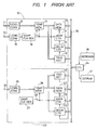
- a state analysis section 10 is supplied at an input port 11 with first input data from a logic circuit under test.
- the first input data is loaded as a set logic levels into a temporary memory 13 via a level converter 12 for removing analog components as required.
- Clock pulses synchronized with those of the first input data to the input port 11 and qualifiers indicating change portions of the data are applied to an input port 14.
- the input external clock pulses synchronized with the data and the qualifiers are similarly converted by a level converter 15 to logic levels for input into a sampling clock generator 16.
- the sampling clock generator 16 creates sampling clock pulses 17 corresponding to the change portions of the first input data.
- the data from the level converter 12 is loaded into the temporary memory 13.
- the first input data to the input port 11, the clock pulses synchronized therewith and the qualifiers are such as shown in Figs. 2A, B and C, respectively, and the sampling clock pulses have a one-to-one correspondence to the first input data, as depicted in Fig. 2D.
- the output of the temporary memory 13 is applied to a data memory 18 and a trigger detector 19.
- the sampling clock pulses 17 are provided to an address counter 21 wherein they are counted.
- the data from the temporary memory 13 is written into the data memory 18 which is addressed by the count value of the address counter 21.
- the address of the address counter 21 is updated after the write is effected in the data memory 18.
- the address counter 21 and the data memory 18 have addresses of the same number, and when the address counter 21 overflows, the write is effected again in the data memory 18 starting at the zero address. In this way, the data memory 18 is successively supplied with the first input data from the input port 11.
- the trigger detector 19 has set therein trigger data, and when the input data from the temporary memory 13 matches the set trigger data, a delay counter 22 serving as a delay means starts to count the sampling clock pulses 17.
- the delay counter 22 overflows, that is, yields a delayed output, by which the address counter 21 is stopped from counting, that is, the data input to the data memory 18 is stopped.
- input data which precedes and follows the same data as the set data (the trigger data) are loaded into the data memory 18.
- a timing analysis section 23 is supplied with second input data from a second data input port 24.
- the second input data is converted by a level converter 25 to a logic level and then input into a temporary memory 26.
- the write in the temporary memory 26 is effected by an internal sampling clock. That is, the second input data from the level converter 25 is loaded into the temporary memory 26 by sampling clock pulses 28 of a fixed frequency which is available from a sampling clock generator 27.
- the sampling clock pulses 28 are supplied as well to an address counter 29, by which they are counted.
- the output of the temporary memory 26 is provided to a data memory 31 and a trigger detector 32. Upon each occurrence of the sampling clock 28, the output of the temporary memory 26 is stored in the data memory 31 which is addressed according to the count value of the address counter 29.
- the trigger detector 32 detects agreement between its set trigger data and the output of the temporary memory 26. When they match, a delay counter 33 as a delay means starts its operation to count the sampling clock pulses 28. Having counted clock pulses of a number corresponding to a present delay, the delay counter 33 overflows, that is, produces an output, by which the counting operation of the address counter 29 is stopped.
- a control section 34 which is equipped with a microcomputer, for instance, is connected via an interface bus 35 with the data memories 18 and 31, the trigger detectors 19 and 32, the address counters 21 and 29 and the delay counters 22 and 33.
- the control section 34 is able to set data to be triggered (trigger data) in the trigger detectors 19 and 32, to read out the stored contents of the data memories 18 and 31 controlling the address counters 21 and 29 and to set delay data in the delay counters 22 and 33.
- the trigger data and delay data are entered through a keyboard (input means) 36, and they are set in the trigger detectors and the delay counters under control of the control section 34.
- the stored contents of the data memories 18 and 31 can be displayed on a display device 37.
- the first and second input data before and after the detection of the set trigger data of the trigger detectors 19 and 32 are stored in the data memories 18 and 31, and either one of the data is displayed on the display device 27.
- the display device 27 For example, in the case of displaying the stored contents of the data memory 18, data indicating various states of program are displayed in the respective lines on a display screen 37a, the trigger data set in the trigger detector 19, that is, the trigger position is indicated by a lateral marker 38 and the states before and after the preset trigger data, for example, steps of the program are sequentially displayed, as shown in Fig. 3A.
- the stored contents of the data memory 31 in the timing analysis section 23 are displayed on the display screen 37a of the display device 37, as depicted in Fig. 3B.
- the states of outputs of the logic circuit are displayed with the lateral direction as the time axis, and the logic outputs of respective parts are arranged in the vertical direction.
- the trigger data detected by the trigger detector 32 corresponds to a set of those logic states on a broken line marker 39 in the vertical direction, that is, in a direction perpendicular to the time axis.
- the data of the data memory 18 in the state analysis section 10 and the data of the data memory 31 in the timing analysis section 23 are selectively displayed on the display device 37, one at a time through manipulation of the keyboard 36, as described above.
- the first input data to the input port 11 and the second input data to the input port 24 will correspond to each other at the time of trigger generation by the trigger detectors 29 and 32. Accordingly, the status (data) indicated by the trigger marker 38 in the data display of the state analysis section 10 and the data indicated by the trigger marker 39 in the display of the timing analysis section 23 can be correlated to each other.
- the state analysis section 10 inputs data, for example, upon each change in the address or status data, as described previously, and the time axis in the vertical direction in Fig. 3A is not always graduated at regular intervals, in other words, the time intervals between data displayed at adjacent lines are usually not fixed.
- the display in Fig. 3A merely indicates data in order of l occurrence not in terms of time.
- the data displayed on the display device 37 is selectively read out specifying a desired place with a cursor.
- the state analysis section 10 and the timing analysis section 23 are both provided, or where two state analysis sections are provided, it would be very convenient if such a desired part of data of one analysis section specified by the cursor and that part of data of the other analysis section corresponding thereto in time could be displayed simultaneously. But the conventional logic analyzer has no such capability.
- the loading intervals are measured by a first interval measuring circuit and stored in a first input interval memory.
- the time interval between delayed outputs of first and second delay means which delay outputs of first and second trigger detectors, that is, the time difference between points of stopping the data input to first and second data memories is measured by a time difference measuring circuit and stored in a time difference memory.
- the time interval between the input stop point of the data memory having stored therein the specified data and the input stop point of the specified data is obtained as a reference time interval, and a value m is determined such that the sum of the time interval from the input stop point of the other data memory back to the input point of the Kth previous data and the time difference, including its sign, between the input stop points of the both data memories will be close to the reference time interval, and the Kth previous data is used as the corresponding data.
- the corresponding data is indicated by another cursor and the respective data of the first and second data memories are simultaneously displayed in first and second display areas, thereby providing a clear indication of the relationship between the specified data and the corresponding data. It is also possible that when the screen of one of the display area is scrolled, the screen of the other display area is also scrolled in association therewith so that temporally corresponding data may always be displayed in the both display areas at predetermined positions respectively.
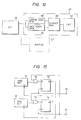
- Fig. 4 illustrates an embodiment of the logic analyzer of the present invention, which is provided with two state analysis sections 10 and 41.
- a second state analysis section 41 is supplied at the input port 24 with the second input data.
- a clock and a qualifier synchronized with the second input data are provided to an input port 42 and converted by a level converter 42 to logic levels, thereafter being applied to a sampling clock generator 44.
- the sampling clock generator 44 creates the sampling clock pulses 28 using the qualifier only when the second input data from the input port 24 changes, as is the case with the sampling clock generator 16 in the state analysis section 10. Accordingly, the second input data is stored in the temporary memory 26 only when the data changes.
- the successive loading intervals of the stored data are measured by loading interval measuring circuits 45 and 46, respectively.
- the thus measured loading intervals are the pulse intervals of the sampling clock pulses 17 and 28.
- an interval measuring counter is used in each of the interval measuring circuits 45 and 46. Reference clock signals from a clock generator 47 are counted by the interval measuring counters in the interval measuring circuits 45 and 46, respectively.
- the interval measuring counters are reset by the sampling clock pulses 17 and 28, and their count values immediately before their resetting are output as the loading intervals.
- the loading intervals of the first and second input data are measured by the interval measuring circuits 45 and 46, respectively, and these measured loading intervals are stored in loading interval memories 48 and 49 using the count values of the address counters 21 and 29 as addresses therefor. That is to say, the input interval data thus stored in the input interval memories 48 and 49 have a one-to-one correspondence to the data stored in the data memories 18 and 31 at the same addresses as those in the memories 48 and 49.
- the time difference between the time of stopping the writing in the data memories 18 and 31 is measured by applying the outputs of the delay counters 22 and 33 to a time difference measuring circuit 51.
- the reference clock signal from the clock generator 47 is provided to the time difference measuring circuit 51 to measure the abovesaid time difference, and the measured time difference is stored in a time difference memory 52.
- the time difference measuring circuit 51 is arranged so that the measured time difference is accompanied by a signal indicating which of them was applied earlier.
- the time difference measuring circuit 51 has such a circuit arrangement as shown in Fig. 5, for instance.
- the outputs of the delay counters 22 and 33 are applied to input terminals 53 and 54, from which they are supplied to an exclusive OR circuit 55.
- the output of the exclusive OR circuit 55 is provided to set and reset terminals of an RS flip-flop 57 via AND circuits 56a and 56b, which are supplied with Q and Q outputs of the flip-flop 57, respectively.
- An earlier one of the inputs from the terminals 53 and 54 is provided via the exclusive OR circuit 55 and the AND circuit 56a to the flip-flop 57 (initially reset) to set it, and by its Q output, a gate 58 is enabled.
- the reference clock pulses from the reference clock generator 47 are applied via the gate 58 to a time counter 59 for counting.
- the other of the inputs from the terminals 53 and 54 is supplied via the exclusive OR circuit 55 and the AND circuit 56b to the flip-flop 57, resetting it. In this way, the time difference between the two inputs, i.e. the time difference in occurrence between the outputs of the delay counters 22 and 23 is obtained as the count value of the time counter 59.
- an RS flip-flop 61 is set by the input from the terminal 53, and is reset by the input from the terminal 54.
- the Q output of the flip-flop 61 is delivered, as a sign bit for the count value of the time counter 59, from a terminal 62. That is, when the input from the terminal 53 is earlier than the input from the terminal 54, the flip-flop 61 is set simultaneously with the starting of the counter 59 and then reset upon completion of the counting operation of the counter 59 and its Q output is derived as a high level at the terminal 62. Similarly, when the input from the terminal 54 is earlier than the input from the terminal 53, the Q output of the flip-flop 61 is provided as a low level upon completion of the counting of the counter 59.
- the inputs to the terminals 53 and 54 are selected short in duration so that they may not overlap each other in time.
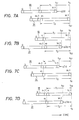
- the data memory 18 holds the oldest data at its address 0 and the newest data at its last address N-l, as depicted in Fig. 6A.
- ⁇ t 10 is stored in the loading interval memory 48 at the address 0, but this is an insignificant data.
- the contents of these loading interval memories for example, ⁇ t ln is the time interval between adjacent two sampling clock pulses for loading the first input data into the loading interval memory 48 at the addresses (n-1) and n, respectively.
- Fig. 7A shows the stored contents of the data memories 18 and 31 along time axis so that the positions in an axial direction of those addresses 0, n, N-1, m-1, m and M-1 may roughly indicate the respective input data loading times at those addresses of the data memories 18 and 31.
- This example shows the case where the load-stop time t s2 of the data memory 31 succeeds the load-stop time t s1 of the data memory 18, and the time difference ⁇ Td between them is stored in the time difference memory 48.
- a desired one of the data stored in one of the data memories 18 and 31 is specified by the keyboard (input means) 36
- data stored in the other data memory is detected which was loaded at the time close to the time of loading of the specified data. For instance, when a cursor is positioned to specify a data on the display read out from the address n of the data memory 18 in Fig. 7A, data at the address m-1 (or m) of the data memory 31 is detected which was stored at a time close to that when the data at the address n of the data memory 18 was stored.
- Fig. 7A illustrates memory locations of the data memories 18 and 31 with their last addresses N-1 and M-1 held in correspondence to their write stopping points t s1 and ts2, respectively. The following procedure is used for obtaining data in the one of the data memories which was loaded at the closest time of loading of the specified data in the other data memory.
- step S 1 a check is made to determine if the mode of operation is a concurrent cursor mode in which when the data in one of the data memories 18 and 31 is specified, data corresponding in loading time to the specified data is detected from the other data memory. If not, the process is immediately finished. If yes, however, the position of specifying the data in the data memory 18, i.e. the posigion of indication by a first cursor, entered through the keyboard 36, is read out in step S 2 .
- step S 3 the time difference between the later one of the data write stopping points t 1 and t 2 and the time of loading of the data at the position of the first cursor is obtained as a reference time interval T 1 .
- the reference time interval T 1 is obtained from the following expression (I):
- the reference time interval T 1 is obtained from the following expression (2):
- the first term on the right side of the expression (1) and expression (2) are each the sum of successive data sampling intervals from the last data storing address N-1 to the address n of the data memory 18 specified by the first cursor, and this is obtained by adding together respective measured interval data from the address N-l to the address n of the input interval memory 48.
- a value m is obtained such that the input data loading time t 1n at the address n may be intermediate between the input data loading time t 2m and t 2(m-1) of data at addresses m and m-1 of the data memory 31.
- the value m is determined which provides those two values of the time interval between the sampling time of a data in the data memory 31 and the later one of the input data load stop points, which two values are immediately above and below the reference time interval T 1 respectively.
- the value m is obtained that satisfies the following expression (3):
- the value of ⁇ t 2i are obtained successively from the interval memory 49. Namely, the measured time intervals ⁇ t 2m stored in the interval memory 49 are sequentially added starting with the one in the last address M-1, obtaining an address m-1 when the sum value exceeds T 1 and the immediately preceding address m.
- the value m is obtained that satisfies the following expression (4):
- the stop time t s2 is later than the other stop time t s1 (Fig. 7A)
- the following expression (5) is used as an expression for decision
- Fig. 7B the following expression (6) is used.
- the time difference between the data loading time t 2m at the address m and the later data load stop time t s is set as T 2 in step S 6 .
- the time difference between the input data loading time t 2(m-1) at the address m-1 and the later stop point t s is set as T 2 in step S 7 .
- step S 6 the computation of the following expression (7) or (8) is conducted depending upon whether the input stop point t s2 is later or earlier than the other stop point t sl :
- step S 7 the following expression (9) or (10) is computed depending upon whether the input stop point t s2 is later or earlier than the other stop point t s1 :
- step S 8 it is checked whether or not the data at the address m or m-1 of the data memory 31 is being displayed on the display screen of the display device.
- the display device 37 does not display all the data of either data memory 18 or 31, but displays only those portions of the data before and after the trigger marker. Accordingly, the data in the data memory 31 corresponding to the data specified by the first cursor is not always displayed on the display screen of the display device 37.
- step S 9 the data is input into the display device 37 from the data memory 31 in step S 9 so that the data corresponding to the time interval T 1 may be displayed on the display device 37.
- step S 10 a second cursor is moved to the position of the data corresponding to the time interval T 2 on the display screen, that is, to the position of the data read out from the address m or m-1 in the data memory 31, after which the process returns to step S 1 .
- the data of the data memories 18 and 31 may also be displayed alternately on one display screen, as referred to previously in connection with Fig. 3.
- a relatively wide display screen is used as the display screen 37a of the display device 37 and the display screen 37a is divided into left and right display areas 37b and 37c, on which the data of the data memories 18 and 31 are displayed and the trigger data set by the trigger detectors 19 and 32 are indicated by the trigger markers 38 and 39, respectively.
- the specified data in the data memory 18 is indicated by the first cursor 63 in the display area 47c and the data at the address m or m-1 of the data memory 31, corresponding to the time interval T 2 is similarly indicated by the second cursor 64 in the display area 37d.
- the cursors 63 and 64 immediately provide a clear indication of the temporal relationship between different data delivered from the input ports 11 and 24.
- the data input from the controller 34 is stored, for example, in a data video memory 65, as shown in Fig. 10.
- data representing character and/or symbols to be displayed at respective parts in the display areas 37b and 37c are stored in the video memory 65 at addresses corresponding to the display positions in the display area.
- data representing the trigger markers 38 and 39 and the cursors 63 and 64 are stored in a cursor video memory 66 at addresses corresponding to the display positions in the display area.
- the video memories 65 and 66 are read out in synchronism with the scanning of the dispiay screen of a cathode ray tube display (a so-called CRT display) 67, and their outputs are provided to a code pattern converter 68 (a so-called character generator), wherein the data such as a character or symbol is converted to dot data for input as display data into the display 67.
- a code pattern converter 68 a so-called character generator
- step S 1 a check is made to determine if the mode of operation is the concurrent cursor mode, and if so, the address m in the data memory 31 specified by the second cursor 46 is read out in step S 2 .
- step S 3 a time difference between the later one of the input data load stop points t s1 and t s2 and the input data loading time t 2m at the specified address m is obtained as the reference time interval T 2 .
- This operation is conducted using the following expression (11) or (12) in dependence upon whether the input data load stop point t s2 is later (Fig. 7C) or earlier (Fig. 7D) than the other stop point t sl :
- step S 4 such a value n is determined that satisfies t 1(n-1) ⁇ t 2m ⁇ t ln' that is, the reference time interval T 2 may be between the two time intervals from the reference point t s (i.e. later one of the stop points t s1 and ts2) to the respective input data loading points t 1n and t 1(n-1) at the addresses n and n-1. That is to say, the value n is obtained which satisfies the following expression (13) or (14) depending on whether the input data load stop point t s2 is later or earlier than the other stop point t .:
- step S 5 it is checked whether or not the data loading time t 1(n-1) at the address n-1 is closer to the data loading time t 2m at the address m than the data loading time t 1n at the address n is close to. That is, it is checked whether the following expression (15) holds when the input data load stop point t s2 is later than the other stop point t sl , and whether the following expression (16) holds when the input data load stop point t s1 is later than the other stop point t s2 :
- step S 6 When the data loading time t 1n at the address n is closer to the data loading time t 2m at the address m, the difference between the reference time t s and the data loading time t 1n at the address n is set as T 1 in step S 6 .
- This operation is conducted using the following expression (17) or (18) depending upon whether the data load stop point t s2 is later or earlier than the other stop point t sl :
- step S 5 where it is decided in step S 5 that the data loading time t 1(n-1) at the address n-1 is closer to the data loading time t 2m at the address m, the difference between the data loading time t 1(n-1) at the address n-1 and the reference time t s is used as T 1 in step 7.
- This operation is conducted using the following expression (19) or (20) depending upon whether the data load stop point t s2 is later or earlier than the other stop point t sl :
- step S 8 it is checked whether or not data corresponding to T 1 is being displayed on the display screen. If not, the corresponding data is input from the data memory 18 into the display device in step S 9 and, in step S 10 , the first cursor 63 is positioned at the data corresponding to the time T 1 . Incidentally, the operation shown in Fig. 8 or 11 is initiated after deciding whether the first cursor indication is provided for the data of the data memory 18 or 31.
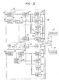
- the present invention is applicable as well to the case of employing the state analysis section 10 and the timing analysis section 23, as shown in Fig. 12 in which the parts corresponding to those in Figs. 4 and 1 are identified by the same reference numerals.
- the level converter 43, the sampling clock generator 44, the interval measuring circuit 46 and the interval memory 49 in Fig. 4 are omitted but the sampling clock generator 27 is employed as in the case of Fig. 1.
- the frequency of the sampling clock 28 is variable and the sampling clock 28 is obtained using the reference clock signal from the clock generator 47 as a reference. Data for displaying such state analysis data as shown in Fig.
- the state analysis data is displayed in the display area 37b of the display screen 37a with the time axis held in the vertical direction and the timing analysis data in the display area 37c with the time axis in the horizontal direction, as depicted in Fig. 9B.
- the trigger marker 38 is displayed as a horizontal line and the first cursor 63 is also displayed sideways, whereas in the display area 37c the trigger marker 39 is displayed as a vertical line and the second cursor 64 is also displayed pointing downward.
- This embodiment also involves the computation of ⁇ t 2i in the operation for obtaining the corresponding data as in the foregoing embodiments. Since the period of the sampling clock 28 (the data input period of the input port 24) is a constant value ⁇ t 2 , however, ⁇ t 2i in the processes shown in Figs. 8 and 11 assumes the constant value dt 2 . Accordingly, it is necessary only to obtain the address m or m-1, or n or n-1 through use of the constant ⁇ t 2i following the procedure depicted in Fig. 8 or 11. Moreover, since At 2i is fixed, the interval measuring circuit 46 and the input interval memory 49 can be left out.
- step S3 the following expression (21) or (22) is used depending upon whether the input data load stop point t s2 is later (Fig. 7A) or earlier (Fig. 7B) than the other stop point t s1 :
- step S 4 the following expression (23) or (24) is used depending upon whether the input data load stop point t s2 is later or earlier than the other stop point t s1 :
- step S 5 the following expression (25) or (26) is used depending upon whether the input data load stop point t s2 is later or earlier than the other stop point tsl:
- step S 6 the following expression (27) or (28) is used depending upon whether the input data load stop point t s2 is later or earlier than the other stop point t s1 :
- step S 7 the following expression (29) or (30) is used depending upon whether the input data load stop point t s2 is later or earlier than the other stop point t sl :
- step S 3 the following expression (31) or (32) is used depending upon whether the input data load stop point t s2 is later or earlier than the other stop point t sl:
- step S 4 the following expression (33) or (34) is used depending upon whether the input data load stop point t S2 is later or earlier than the other stop point t s1 :
- step S 5 the following expression (35) or (36) is used depending upon whether the input data load stop point t s2 is later or earlier than the other stop point t sl:
- step S 6 the following expression (37) or (38) is used depending upon whether the input data load stop point t s2 is later or earlier than the other stop point t sl :
- step S 7 the follbwing expression (39) or (40) is used depending upon whether the input data load stop point t s2 is later or earlier than the other stop point t s1 :
- the reference time interval T s is given as follows:
- ⁇ Td is a value including its sign.
- a sign bit at a terminal 62 in Fig. 5 goes to "1", in which case the absolute value of ⁇ Td is subtracted in the expression (42).
- the sign bit at the terminal 62 goes to "0", in which case the absolute value of ⁇ Td is added in the expression (42). Also in the cases of Figs.
- the data corresponding to the specified data in the data s memory 18 can similarly be indicated using, as the reference time interval, the difference between the reference time t s and the specified data loading time.
- the data stored in one of the data memories 18 and 31 is specified by a cursor
- the corresponding data i.e. data corresponding to the time T 2 in Fig. 8 (data corresponding to the time T 1 in Fig. 11) is delivered to the outside and the data corresponding to the time T 2 (or T 1 ) is specified by the cursor.
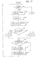
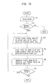
- step S 1 the operator's input mode is read out and it is checked in step S 2 whether the input mode is the concurrent cursor mode. If so, then the first cursor 63 is displayed on the display area 37b (Fig. 9B) in step S 3 . This display is provided at a position set in the previous cycle of operation, or at a predetermined initial position.
- step S 4 an external command, for instance, a move command for the first cursor 63 by the operation of the keyboard 36, is read.
- step S 5 T 1 is computed relative to the commanded position of the first cursor 63, as described previously with respect to Fig. 8, and then T 2 is calculated, determining the corresponding data to be displayed in the display area 37c.
- step S 6 the corresponding data in the display area 37c is indicated by the second cursor 64.
- data in the video memory 65 (in Fig. 10) for " the data memory 31 is updated in step S 7 so that the data to be indicated by the second cursor 64 is displayed.
- step S 8 it is checked whether the concurrent cursor mode is still retained, and if so, the process returns to step S 3 .
- a scroll mode in which data in the data memory 18 or 31 is manually or automatically delivered one by one to the display device 37 to sequentially scroll the data on its display screen.
- a scroll mode in which data in the data memory 18 or 31 is manually or automatically delivered one by one to the display device 37 to sequentially scroll the data on its display screen.
- ste S 1 the operator's set mode of operation is read and it is checked in step S 2 whether it is a concurrent scroll mode.
- step 8 4 a search is made in the data memory 31 for data of the same loading time as that of the data being scrolled on the display area 37b. This operation is carried out in the same manner as described previously with regard to Fig. 8 (or Fig. 11). In such a case, for example, the data (the address) at the center of the display area 37b in the time-axis direction is processed as the address n specified by the first cursor 63.
- step S 5 the corresponding area of the video memory 65 is updated so that the data may be displayed in the display area 37c.
- step S 6 it is checked whether the concurrent scroll mode is still retained, and if so, the process returns to step S 3 .
- the keyboard 36 has mounted thereon a key 71 for selecting the concurrent cursor mode, a key 72 for selecting the concurrent scroll mode, a data/cursor switching key 73 and a key 74 for moving data or cursor on the display screen 37a in the horizontal or vertical direction.
- the keyboard 36 further includes a ten-key pad for setting trigger data and a delay time, as referred to previously, and other function keys.
- a memory in the controller 34 may also be employed.
- the display screen 37a need not always be divided into the display areas 47b and 47c but it is also possible to connect a display device 37' to the controller 34, as shown in Fig. 10, so that the contents of the data memories 18 and 31 are displayed on the display screens of the display devices 37 and 37'.
- the present invention is applicable to the simultaneous display of state analysis data and timing analysis data but also the simultaneous display of data when the two analysis sections are both for state analysis.
- the present invention is applicable not only to the case where data of one of the data memories 18 and 31 is specified and the data in the other data memory corresponding in time to the specified data is displayed, but also to the case where data in one of the two data memories is specified, for example, by an external electronic computer and the temporally corresponding data is delivered from the other data memory.
- step 8 5 it is also possible to omit step 8 5 and perform only step S 6 (or S 7 ) at all times. Furthermore, it is possible to provide three or more analysis sections and utilize the concurrent cursor mode or concurrent scroll mode in displaying their data.
- a trigger priority means is provided so that after a specified one of the trigger detectors yields the detected output, the other trigger detector is allowed to operate.
- a first trigger priority command is applied to a terminal 72.
- the command sets a flip-flop 74 via an OR circuit 73 to make the Q output of the flip-flop 74 high-level and the high-level output is provided to an enable terminal E of the trigger word detector 19, putting it in operation.
- the first trigger priority command at the terminal 72 is provided as well to a reset terminal R of a flip-flop 75 to reset it to make its Q output low-level, and this low-level output is applied to an enable terminal E of the trigger detector 32, putting it out of operation.
- the trigger detector 32 In this state, even if the trigger detector 32 is supplied with the same data as its set data, it will not create its detected output.
- the trigger detector 19 When the trigger detector 19 is supplied with the same data as its set data, it yields the detected output, which is applied via an OR circuit 76 to the flip-flop 75 to set it. In consequence, the trigger detector 32 enters its operative state.
- the trigger detector 32 performs the trigger detecting operation after the trigger detector 19 detect a trigger data.
- a second trigger priority command which is provided to a terminal 77, resets the flip-flop 74 and sets the flip-flop 75 via the OR circuit 76. Accordingly, the trigger detector 32 is made operative but the trigger detector 19 inoperative. In this state, when the trigger detector 32 produces its detected output, it is provided via the OR circuit 73 to the set terminal of the flip-flop 74.
- temporally corresponding data in the other data memory is automatically specified, so that the temporal correspondence between data of the plurality of analysis sections can easily be discerned, greatly facilitating the analysis.
- the temporal correspondence between data indicating each step of a program i.e. a display of a state analysis and signal waveforms, i.e. a display of a timing analysis can easily be recognized. This permits accurate and easy analysis of a logic circuit.
- the states of the plurality of analysis sections are simultaneously displayed, and when the cursor in one of display areas is moved to a desired position, the cursor in the other display area is automatically moved to the temporally corresponding position. Further, when the screen of one of the display areas is scrolled, the screen of the other display area is also scrolled.
- the logic analyzer of the present invention which is equipped with these functions, is of great utility in the analysis of logic circuits.
Landscapes
- Engineering & Computer Science (AREA)
- General Engineering & Computer Science (AREA)
- Physics & Mathematics (AREA)
- General Physics & Mathematics (AREA)
- Theoretical Computer Science (AREA)
- Computer Hardware Design (AREA)
- Quality & Reliability (AREA)
- Test And Diagnosis Of Digital Computers (AREA)
Applications Claiming Priority (2)
| Application Number | Priority Date | Filing Date | Title |
|---|---|---|---|
| JP238994/84 | 1984-11-12 | ||
| JP23899484 | 1984-11-12 |
Publications (3)
| Publication Number | Publication Date |
|---|---|
| EP0181619A2 true EP0181619A2 (de) | 1986-05-21 |
| EP0181619A3 EP0181619A3 (en) | 1988-07-13 |
| EP0181619B1 EP0181619B1 (de) | 1993-10-13 |
Family
ID=17038330
Family Applications (1)
| Application Number | Title | Priority Date | Filing Date |
|---|---|---|---|
| EP85114242A Expired - Lifetime EP0181619B1 (de) | 1984-11-12 | 1985-11-08 | Logikanalysator |
Country Status (4)
| Country | Link |
|---|---|
| US (1) | US4730314A (de) |
| EP (1) | EP0181619B1 (de) |
| JP (1) | JPS61269073A (de) |
| DE (1) | DE3587625D1 (de) |
Cited By (2)
| Publication number | Priority date | Publication date | Assignee | Title |
|---|---|---|---|---|
| EP0318768A1 (de) * | 1987-11-30 | 1989-06-07 | Kontron Elektronik Gmbh | Logikanalysator |
| WO2004099987A1 (en) * | 2003-04-08 | 2004-11-18 | Zeroplus Technology Co., Ltd | Logic analyzer data retrieving circuit and its retrieving method |
Families Citing this family (16)
| Publication number | Priority date | Publication date | Assignee | Title |
|---|---|---|---|---|
| US4817118A (en) * | 1987-06-29 | 1989-03-28 | Step Engineering | Mobile incident logger |
| US4965800A (en) * | 1988-10-11 | 1990-10-23 | Farnbach William A | Digital signal fault detector |
| US5282213A (en) * | 1991-01-02 | 1994-01-25 | Compaq Computer Corporation | Computer-based logic analyzer timing and analysis system |
| US5886660A (en) * | 1997-10-28 | 1999-03-23 | National Instruments Corporation | Time-to-digital converter using time stamp extrapolation |
| US6396517B1 (en) | 1999-03-01 | 2002-05-28 | Agilent Technologies, Inc. | Integrated trigger function display system and methodology for trigger definition development in a signal measurement system having a graphical user interface |
| US6279130B1 (en) * | 1999-04-30 | 2001-08-21 | Tektronix, Inc. | External trigger delay compensation apparatus |
| DE10127656B4 (de) * | 2001-06-07 | 2008-09-18 | Qimonda Ag | Vorrichtung und Verfahren zur Untersuchung des Signalverhaltens von Halbleiterschaltungen |
| US7409617B2 (en) * | 2004-09-30 | 2008-08-05 | Credence Systems Corporation | System for measuring characteristics of a digital signal |
| US7627790B2 (en) * | 2003-08-21 | 2009-12-01 | Credence Systems Corporation | Apparatus for jitter testing an IC |
| TW201213826A (en) * | 2010-09-16 | 2012-04-01 | Peregrine Technology Co Ltd | Data preview device of logic analyzer and method thereof |
| US9557876B2 (en) | 2012-02-01 | 2017-01-31 | Facebook, Inc. | Hierarchical user interface |
| US9229613B2 (en) | 2012-02-01 | 2016-01-05 | Facebook, Inc. | Transitions among hierarchical user interface components |
| US9645724B2 (en) | 2012-02-01 | 2017-05-09 | Facebook, Inc. | Timeline based content organization |
| US9405759B2 (en) * | 2013-11-20 | 2016-08-02 | Lenovo (Beijing) Co., Ltd. | Information processing method and electronic device |
| GB2526850B (en) * | 2014-06-05 | 2020-11-25 | Advanced Risc Mach Ltd | Logic analyzer |
| JP7552643B2 (ja) * | 2022-03-30 | 2024-09-18 | 横河電機株式会社 | データ処理装置、データ処理方法、及びプログラム |
Family Cites Families (9)
| Publication number | Priority date | Publication date | Assignee | Title |
|---|---|---|---|---|
| JPS5813864B2 (ja) * | 1979-11-26 | 1983-03-16 | 岩崎通信機株式会社 | ロジツク信号観測装置 |
| US4541100A (en) * | 1981-05-15 | 1985-09-10 | Tektronix, Inc. | Apparatus including a programmable set-up and hold feature |
| JPS6030898B2 (ja) * | 1981-05-15 | 1985-07-19 | テクトロニクス・インコ−ポレイテツド | ロジツク・アナライザの入力装置 |
| US4434488A (en) * | 1981-06-08 | 1984-02-28 | Tektronix, Inc. | Logic analyzer for a multiplexed digital bus |
| US4425643A (en) * | 1981-06-08 | 1984-01-10 | Tektronix, Inc. | Multi-speed logic analyzer |
| DE3132984A1 (de) * | 1981-08-20 | 1983-03-10 | Siemens AG, 1000 Berlin und 8000 München | Logikanalysator |
| EP0094976B1 (de) * | 1982-05-24 | 1986-08-27 | Ibm Deutschland Gmbh | Logik-Analysator |
| US4538235A (en) * | 1982-08-19 | 1985-08-27 | Rockwell International Corporation | Microcomputer retriggerable interval counter |
| US4558422A (en) * | 1983-03-23 | 1985-12-10 | Tektronix, Inc. | Digital signal sampling system with two unrelated sampling timebases |
-
1985
- 1985-11-08 DE DE85114242T patent/DE3587625D1/de not_active Expired - Lifetime
- 1985-11-08 EP EP85114242A patent/EP0181619B1/de not_active Expired - Lifetime
- 1985-11-11 JP JP60252572A patent/JPS61269073A/ja active Pending
- 1985-11-12 US US06/797,205 patent/US4730314A/en not_active Expired - Fee Related
Cited By (4)
| Publication number | Priority date | Publication date | Assignee | Title |
|---|---|---|---|---|
| EP0318768A1 (de) * | 1987-11-30 | 1989-06-07 | Kontron Elektronik Gmbh | Logikanalysator |
| US4924468A (en) * | 1987-11-30 | 1990-05-08 | Kontron Holding Ag | Logic analyzer |
| WO2004099987A1 (en) * | 2003-04-08 | 2004-11-18 | Zeroplus Technology Co., Ltd | Logic analyzer data retrieving circuit and its retrieving method |
| CN100458711C (zh) * | 2003-04-08 | 2009-02-04 | 孕龙科技股份有限公司 | 逻辑分析仪的资料撷取处理方法及其装置 |
Also Published As
| Publication number | Publication date |
|---|---|
| JPS61269073A (ja) | 1986-11-28 |
| EP0181619A3 (en) | 1988-07-13 |
| EP0181619B1 (de) | 1993-10-13 |
| DE3587625D1 (de) | 1993-11-18 |
| US4730314A (en) | 1988-03-08 |
Similar Documents
| Publication | Publication Date | Title |
|---|---|---|
| EP0181619A2 (de) | Logikanalysator | |
| US4425643A (en) | Multi-speed logic analyzer | |
| JP2733746B2 (ja) | ロジック信号表示方法 | |
| US4495621A (en) | Glitch detecting and measuring apparatus | |
| JPH0549818B2 (de) | ||
| CA1172361A (en) | Logic analyzer for a multiplexed digital bus | |
| EP2829883A1 (de) | Schaltverlustmessung und Zeichnung in einem Prüf- und Messinstrument | |
| US4381563A (en) | Apparatus and method for visually presenting analytical representations of digital signals | |
| EP0163267B1 (de) | Logikanalysator | |
| US6279130B1 (en) | External trigger delay compensation apparatus | |
| US4578666A (en) | Method of comparing data with asynchronous timebases | |
| CA1151329A (en) | Method of displaying logic signals for a logic signal measurement apparatus | |
| EP0004153A1 (de) | Methode und Vorrichtung zum Vergleich logischer Funktionen | |
| JPS59188564A (ja) | 複数の操作レベルを有する測定機器 | |
| JPS64664B2 (de) | ||
| JPS6350668B2 (de) | ||
| JPH0614102B2 (ja) | 回路試験装置 | |
| SU444189A1 (ru) | Устройство дл контрол и классификации полупроводниковых приборов | |
| JP2000147018A (ja) | オシロスコープのメニュー階層表示方法及びメニュー階層表示オシロスコープ | |
| JPH03202783A (ja) | ロジックアナライザ | |
| JPS60205638A (ja) | マイクロプロセツサアナライザ | |
| JPH04138374A (ja) | ロジックアナライザ | |
| JPS63186153A (ja) | ロジツクアナライザ | |
| JPS61114347A (ja) | マイクロプロセツサの処理記憶法 | |
| JPH0424564A (ja) | ロジックアナライザ |
Legal Events
| Date | Code | Title | Description |
|---|---|---|---|
| PUAI | Public reference made under article 153(3) epc to a published international application that has entered the european phase |
Free format text: ORIGINAL CODE: 0009012 |
|
| 17P | Request for examination filed |
Effective date: 19851108 |
|
| AK | Designated contracting states |
Kind code of ref document: A2 Designated state(s): DE GB NL |
|
| PUAL | Search report despatched |
Free format text: ORIGINAL CODE: 0009013 |
|
| AK | Designated contracting states |
Kind code of ref document: A3 Designated state(s): DE GB NL |
|
| 17Q | First examination report despatched |
Effective date: 19910205 |
|
| GRAA | (expected) grant |
Free format text: ORIGINAL CODE: 0009210 |
|
| AK | Designated contracting states |
Kind code of ref document: B1 Designated state(s): DE GB NL |
|
| PG25 | Lapsed in a contracting state [announced via postgrant information from national office to epo] |
Ref country code: NL Effective date: 19931013 Ref country code: DE Effective date: 19931013 |
|
| REF | Corresponds to: |
Ref document number: 3587625 Country of ref document: DE Date of ref document: 19931118 |
|
| PG25 | Lapsed in a contracting state [announced via postgrant information from national office to epo] |
Ref country code: GB Effective date: 19940113 |
|
| NLV1 | Nl: lapsed or annulled due to failure to fulfill the requirements of art. 29p and 29m of the patents act | ||
| PLBE | No opposition filed within time limit |
Free format text: ORIGINAL CODE: 0009261 |
|
| STAA | Information on the status of an ep patent application or granted ep patent |
Free format text: STATUS: NO OPPOSITION FILED WITHIN TIME LIMIT |
|
| GBPC | Gb: european patent ceased through non-payment of renewal fee |
Effective date: 19940113 |
|
| 26N | No opposition filed |