EP0181784B1 - Erzeugungssystem für Digitalsignale und Verfahren dafür - Google Patents
Erzeugungssystem für Digitalsignale und Verfahren dafür Download PDFInfo
- Publication number
- EP0181784B1 EP0181784B1 EP85308304A EP85308304A EP0181784B1 EP 0181784 B1 EP0181784 B1 EP 0181784B1 EP 85308304 A EP85308304 A EP 85308304A EP 85308304 A EP85308304 A EP 85308304A EP 0181784 B1 EP0181784 B1 EP 0181784B1
- Authority
- EP
- European Patent Office
- Prior art keywords
- signal
- level
- read
- enable
- producing
- Prior art date
- Legal status (The legal status is an assumption and is not a legal conclusion. Google has not performed a legal analysis and makes no representation as to the accuracy of the status listed.)
- Expired - Lifetime
Links
Images

Classifications
-
- G—PHYSICS
- G11—INFORMATION STORAGE
- G11B—INFORMATION STORAGE BASED ON RELATIVE MOVEMENT BETWEEN RECORD CARRIER AND TRANSDUCER
- G11B20/00—Signal processing not specific to the method of recording or reproducing; Circuits therefor
- G11B20/10—Digital recording or reproducing
-
- G—PHYSICS
- G11—INFORMATION STORAGE
- G11B—INFORMATION STORAGE BASED ON RELATIVE MOVEMENT BETWEEN RECORD CARRIER AND TRANSDUCER
- G11B20/00—Signal processing not specific to the method of recording or reproducing; Circuits therefor
- G11B20/10—Digital recording or reproducing
- G11B20/10009—Improvement or modification of read or write signals
Definitions
- the present invention relates generally to a digital signal processing system and method especially adapted for reproducing and wave- shaping digital signals. More specifically, the invention relates to generaion of a read-enable pulse for reproducing digital signals recorded on a magnetic medium, such as a magnetic tape, a magnetic disk and so forth.
- the conventional process for generating read- enable pulses works as long as the pulse intervals of the digital signal remain essentially constant and short enough that the analog reproduced signal is always changing due to magnetic reversals on the medium.
- the intervals between reversals vary significantly.
- the reproduced signal level tends to remain constant at approximately zero for a noticeable period of time before continuing toward the next amplitude peak, this waveform being commonly known as a "shoulder".
- EP-A-84358 refers to monitoring of the reproduced signal level and establishing thresholds which that signal must exceed to perform a quality check of the reproduced signal and thereby produce a read-enable signal.
- the probability of read error is especially high when the reproduced signal is noisy, in particular near shoulders.
- a digital signal processing system monitors variation of the signal level of a reproduced signal and also monitors variation of the differentiated signal level.
- the system generates a read-enable pulse when the reproduced signal level rises or drops across a predetermined threshold level and this is followed by a zero-crossing in the differentiated signal level.
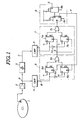
- the preferred embodiment of the digital signal processing system includes a magnetic disk 1 serving as a magnetic recording medium.
- a magnetic head 1a picks up data recorded on the magnetic disk 1.
- the magnetic head 1 a produces a signal representative of the read data, which signal will be referred to hereafter as "reproduced signal A".
- the reproduced signal A is fed to a differentiation circuit 3 and a hysteresis comparator 4.
- the hysteresis comparator 4 has first and second threshold levels Th 1 and Th 2 .
- the first and second threshold levels Th 1 and Th 2 are of opposite sign but have the same absolute values which are selected to be sufficiently far from the zero level of the reproduced signal A to eliminate the influence of shoulders, as explained below.
- the differentiation circuit 3 outputs a signal representative of the differentiated value, which signal will be hereafter referred to as "diffentiated signal C".
- the differentiated signal C is sent to a zero-crossing comparator 5.
- the hysteresis comparator 4 outputs a comparator signal B to an edge-detecting circuit 6.
- the level of the comparator signal B reverses between HIGH and LOW each time the reproduced signal A level raises or drops outside of the range defined by the threshold levels Th 1 and Th 2 .
- the edge-detecting circuit 6 comprises a pair of D-flip-flops 6a and 6b which receive the comparator signal B.
- the edge-detecting circuit 6 also comprises an OR gate 6c and an inverter 6d.
- the inverter 6d is interposed between the hysteresis comparator 4 and the D-flip-flop 6b, whereby it sends the inverted comparator signal B to the latter.
- the zero-crossing comparator 5 sends a comparator signal D to another edge-detecting circuit 7.
- the comparator signal D varies between HIGH and LOW levels. Specifically, the comparator signal D is HIGH while the amplitude of the differentiated signal C is positive and is LOW level while the amplitude of the differentiated signal C is negative.
- the edge-detecting circuit 7 comprises a pair of D-flip-flops 7a and 7b, an OR gate 7c and an inverter 7d.
- the inverter 7d is interposed between the zero-crossing comparator 5 and the D-flip-flop 7b.
- the reset terminals of the D-flip-flops 7a and 7b are connected for input from the OR gate 6c. Therefore, the D-flips-flops 7a and 7b are reset by HIGH level outputs from the OR gate 6c.
- the OR gate 7c is connected for output to a monostable multivibrator 8a in a pulse generator circuit 8.
- the monostable multivibrator 8a has an inverted output terminal connected to the reset terminal of the D-flips-flops 6a and 6b.
- the non-inverted output terminal of the monostable multivibrator 8a is connected to another monostable multivibrator 8b which serves to generate the read-enable pulse G.
- the hysteresis comparator 4 continuously compares the signal level of the reproduced signal A with the threshold levels Th 1 and Th 2 . At a time T 1' the reproduced signal level A increases across the upper threshold level Th 1 . The signal level of the hysteresis comparator 4 then turns from LOW level to HIGH level. The comparator signal level B remains HIGH until the reproduced signal level A drops below the lower threshold level Th 2 . The HIGH level comparator signal B sets the D-flip-flop 6a so that a HIGH-level set signal is sent to the OR gate 6c. At this time, the input level to the D-flip-flop 6b remains LOW.
- the output level of the OR gate 6c goes HIGH to turn the input levels at the reset terminals of the D-flip-flops 7a and 7b LOW. Therefore, the D-flip-flops 7a and 7b are released from their reset states, i.e. they are enabled.
- the D-flip-flops 7a and 7b are responsive to HIGH-level inputs to output HIGH-level set signals.
- the differentiated signal C drops across the zero level, so that the signal level of the zero-crossing comparator 5 goes from HIGH to LOW.
- a HIGH-level signal is input to the D-flip-flop 7b through the inverter 7d. Therefore, the D-flip-flop 7b outputs a HIGH-level set signal to the OR gate 7c.
- the input level to the D-flip-flop 7a remains LOW. Therefore, the output level of the D-flip-flop 7a remains LOW.
- the input level at the reset terminals of the D-flip-flops 6a and 6b go HIGH to reset the latter at the time T 2 .
- the output level at the non-inverted output terminal of the monostable multivibrator 8a goes HIGH to trigger the monostable multivibrator 8b. Therefore, the output G of the monostable multivibrator 8b, which serves as the read- enable pulse, goes HIGH.
- the reproduced signal level A drops below the lower threshold level Th 2 .
- the output level of the hysteresis comparator 4 goes from HIGH to LOW.
- the comparator signal level B remains LOW until the reproduced signal level A rises above the upper threshold level Th 1 .
- the LOW-level comparator signal B is sent to the D-flip-flop 6a and through the inverter 6d to the D-flip-flop 6b.
- This LOW-level input holds the D-flip-flop 6a in its reset state.
- the input level for the D-flip-flop 6b goes HIGH, thus setting the latter. Therefore, the D-flip-flop 6b outputs a HIGH-level set signal to the OR gate 6c.
- the D-flip-flops 7a and 7b are responsive to HIGH-level input at their reset input terminals to be released from the reset state.
- the differentiated signal C rises across the zero-level.
- the signal level of the zero-crossing comparator 5 goes from LOW to HIGH.
- a HIGH-level signal is sent to the D-flip-flop 7a and through the inverter 7d to the D-flip-flop 7b. Therefore, the D-flip-flop 7a outputs a HIGH-level set signal to the OR gate 7c.
- the input level at the D-flip-flop 7b remains LOW. Therefore, the output level of the D-flip-flop 7b remains LOW.
- a HIGH-level signal is transmitted to the monstable multivibrator 8a by the OR gate 7c.
- the output level F at the inverted output terminal of the monostable multivibrator 8b goes LOW. Therefore, the input level at the reset terminals of the D-flip-flips 6a and 6b goes HIGH to reset the latter at the time T 4 .
- the output level at the non-inverted output terminal of the monostable multivibrator 8a goes HIGH to trigger the monostable multivibrator 8b.
- the output G of the monostable multivibrator 8b which serves as the read- enable pulse, goes HIGH.
- a read-enable pulse is again produced in substantially the same manner as disclosed with respect to the period T 1 to T 2 .
- another HIGH-level output 1 2 of the zero-crossing comparator 5 appears but erroneous output of a read- enable pulse is successfully prevented.
- the edge detector 6 is not always necessary for disabling the edge detector 7 but can be replaced with an appropriate gating means for passing and blocking the HIGH-level output of the OR gate 7c to the pulse generator circuit 8.
- the pulse generator circuit 8 may comprise a single monostable multivibrator, in such case, the D-flip-flops 6a and 6b can be reset by the read- enable pulse therefrom.
- the D-flip-flops 6a and 6b can be replaced by an appropriate signal generator which generates a HIGH-level signal to release the D-flip-flops 7a and 7b from their reset state.
- This signal generator can be a monostable multivibrator which continuously outputs a HIGH-level signal for a given period after detecting variation of the reproduced signal level across one of the upper and lower threshold levels Th 1 and Th 2 as discussed previously.
- the D-flip-flops 7a and 7b can be enabled and disabled by setting and resetting an enable flag by which the operation of the edge detector 7 is controlled, according to signal level variation of the reproduced signal and the presence or absence of the read-enable signal.
Landscapes
- Engineering & Computer Science (AREA)
- Signal Processing (AREA)
- Signal Processing For Digital Recording And Reproducing (AREA)
- Digital Magnetic Recording (AREA)
- Mobile Radio Communication Systems (AREA)
- Communication Control (AREA)
- Manipulation Of Pulses (AREA)
Claims (12)
dadurch gekennzeichnet,
gekennzeichnet durch den Verfahrensschritt,
daß anschließend die Erzeugung eines Lese-Freigabe-Impulses (G) in dem Verfahrensschritt
Priority Applications (1)
| Application Number | Priority Date | Filing Date | Title |
|---|---|---|---|
| AT85308304T ATE55843T1 (de) | 1984-11-16 | 1985-11-14 | Erzeugungssystem fuer digitalsignale und verfahren dafuer. |
Applications Claiming Priority (2)
| Application Number | Priority Date | Filing Date | Title |
|---|---|---|---|
| JP59240524A JPS61120380A (ja) | 1984-11-16 | 1984-11-16 | デジタル信号処理回路 |
| JP240524/84 | 1984-11-16 |
Publications (2)
| Publication Number | Publication Date |
|---|---|
| EP0181784A1 EP0181784A1 (de) | 1986-05-21 |
| EP0181784B1 true EP0181784B1 (de) | 1990-08-22 |
Family
ID=17060806
Family Applications (1)
| Application Number | Title | Priority Date | Filing Date |
|---|---|---|---|
| EP85308304A Expired - Lifetime EP0181784B1 (de) | 1984-11-16 | 1985-11-14 | Erzeugungssystem für Digitalsignale und Verfahren dafür |
Country Status (8)
| Country | Link |
|---|---|
| US (1) | US4751591A (de) |
| EP (1) | EP0181784B1 (de) |
| JP (1) | JPS61120380A (de) |
| KR (1) | KR940000974B1 (de) |
| AT (1) | ATE55843T1 (de) |
| AU (1) | AU581267B2 (de) |
| CA (1) | CA1306538C (de) |
| DE (1) | DE3579292D1 (de) |
Families Citing this family (9)
| Publication number | Priority date | Publication date | Assignee | Title |
|---|---|---|---|---|
| US4729045A (en) * | 1986-04-01 | 1988-03-01 | Hewlett-Packard Company | Apparatus and method for digital magnetic recording and reading |
| JPS62275304A (ja) * | 1986-05-22 | 1987-11-30 | Pioneer Electronic Corp | 磁気記録再生装置 |
| US4954903A (en) * | 1987-09-21 | 1990-09-04 | Sharp Kabushiki Kaisha | Digital signal reproduction apparatus for reading magneto-optical disks |
| JPH027234A (ja) * | 1988-02-22 | 1990-01-11 | Hitachi Ltd | 光デイスクのデリートパターン検出回路 |
| US4987500A (en) * | 1988-11-14 | 1991-01-22 | Brier Technology, Inc. | Self compensating high density data recording and detection scheme |
| JPH0786965B2 (ja) * | 1989-08-03 | 1995-09-20 | ローム株式会社 | フロッピーディスク装置用読取り回路 |
| DE69220015T2 (de) * | 1991-12-27 | 1997-09-25 | Matsushita Electric Ind Co Ltd | Optische Platten Lesegerät |
| US5608583A (en) * | 1995-05-24 | 1997-03-04 | Conner Peripherals, Inc. | System for qualifying the detection of a servo dibit |
| CA2656267A1 (en) * | 2006-06-23 | 2008-01-03 | Pixeloptics, Inc. | Electronic adapter for electro-active spectacle lenses |
Family Cites Families (8)
| Publication number | Priority date | Publication date | Assignee | Title |
|---|---|---|---|---|
| US3846829A (en) * | 1972-11-06 | 1974-11-05 | Caelus Memories Inc | Read-write servo track copy system |
| US4345168A (en) * | 1977-02-25 | 1982-08-17 | Fisher Alan J | Electrical peak detector |
| US4135161A (en) * | 1977-05-31 | 1979-01-16 | Torrieri Don J | Method and means for pulse detection |
| DE2729108C3 (de) * | 1977-06-28 | 1980-03-13 | Siemens Ag, 1000 Berlin Und 8000 Muenchen | Schaltungsanordnung zur Erkennung von Taktsignalen und zur Umwandlung in digitale Dauersignale |
| DE3201318A1 (de) * | 1982-01-18 | 1983-07-28 | Tandberg Data A/S, Oslo | Verfahren und schaltungsanordnung zum bewerten von lesesignalen eines magnetschichtspeichers |
| US4467374A (en) * | 1982-04-05 | 1984-08-21 | Hewlett Packard Company | Method and means for direct-current polarity restoration in magnetic recording |
| US4495529A (en) * | 1982-05-07 | 1985-01-22 | Digital Equipment Corporation | Qualifier circuit |
| JPH065593B2 (ja) * | 1982-09-28 | 1994-01-19 | 株式会社東芝 | 磁気ディスク装置のパルス回路 |
-
1984
- 1984-11-16 JP JP59240524A patent/JPS61120380A/ja active Pending
-
1985
- 1985-10-24 KR KR1019850007836A patent/KR940000974B1/ko not_active Expired - Fee Related
- 1985-11-13 US US06/797,499 patent/US4751591A/en not_active Expired - Lifetime
- 1985-11-13 CA CA000495213A patent/CA1306538C/en not_active Expired - Lifetime
- 1985-11-14 EP EP85308304A patent/EP0181784B1/de not_active Expired - Lifetime
- 1985-11-14 DE DE8585308304T patent/DE3579292D1/de not_active Expired - Lifetime
- 1985-11-14 AT AT85308304T patent/ATE55843T1/de not_active IP Right Cessation
- 1985-11-14 AU AU49917/85A patent/AU581267B2/en not_active Ceased
Also Published As
| Publication number | Publication date |
|---|---|
| AU581267B2 (en) | 1989-02-16 |
| JPS61120380A (ja) | 1986-06-07 |
| KR940000974B1 (ko) | 1994-02-07 |
| US4751591A (en) | 1988-06-14 |
| EP0181784A1 (de) | 1986-05-21 |
| KR860004382A (ko) | 1986-06-20 |
| CA1306538C (en) | 1992-08-18 |
| ATE55843T1 (de) | 1990-09-15 |
| DE3579292D1 (de) | 1990-09-27 |
| AU4991785A (en) | 1986-05-22 |
Similar Documents
| Publication | Publication Date | Title |
|---|---|---|
| CA1180110A (en) | Automatic threshold tracking system | |
| JPH0132591B2 (de) | ||
| EP0181784B1 (de) | Erzeugungssystem für Digitalsignale und Verfahren dafür | |
| US4495529A (en) | Qualifier circuit | |
| US4764916A (en) | Reading circuit for an optical disk apparatus | |
| US4417213A (en) | Data regenerative system for NRZ mode signals | |
| US5105316A (en) | Qualification for pulse detecting in a magnetic media data storage system | |
| US4564870A (en) | Signal detector of magnetic disk apparatus | |
| US3622894A (en) | Predetection signal compensation | |
| GB2118403A (en) | Digital signal demodulator circuit | |
| EP0324532B1 (de) | Schwellenwertnachlaufsystem | |
| US3617904A (en) | Noise insensitive peak detector | |
| US4724496A (en) | Peak detector for magnetically recorded binary signal | |
| CA1061893A (en) | Self-clocking, error correcting low bandwidth digital recording system | |
| US3840891A (en) | Time duration modulation and demodulation for storage or transmission of digital data | |
| US3631424A (en) | Binary data detecting apparatus responsive to the change in sign of the slope of a waveform | |
| US4544963A (en) | Read signal detection in ternary 3PM magnetic recording | |
| EP0357046B1 (de) | Signalverarbeitungsanordnung zur Analog-Digital-Wandlung | |
| US4849834A (en) | Read channel architecture for processing read head signals | |
| US4012785A (en) | Magnetic recording playback circuit | |
| US3349389A (en) | Detection system for binary data | |
| US4813059A (en) | Readback recovery of run length limited codes | |
| US3614758A (en) | Method and apparatus for saturation-type digital magnetic recording | |
| US4152731A (en) | Read circuit for distinguishing false peaks in an alternating current playback signal | |
| ES334929A1 (es) | Una disposicion para deteccion de senales binarias. |
Legal Events
| Date | Code | Title | Description |
|---|---|---|---|
| PUAI | Public reference made under article 153(3) epc to a published international application that has entered the european phase |
Free format text: ORIGINAL CODE: 0009012 |
|
| 17P | Request for examination filed |
Effective date: 19851122 |
|
| AK | Designated contracting states |
Kind code of ref document: A1 Designated state(s): AT DE FR GB NL |
|
| 17Q | First examination report despatched |
Effective date: 19880208 |
|
| GRAA | (expected) grant |
Free format text: ORIGINAL CODE: 0009210 |
|
| AK | Designated contracting states |
Kind code of ref document: B1 Designated state(s): AT DE FR GB NL |
|
| REF | Corresponds to: |
Ref document number: 55843 Country of ref document: AT Date of ref document: 19900915 Kind code of ref document: T |
|
| REF | Corresponds to: |
Ref document number: 3579292 Country of ref document: DE Date of ref document: 19900927 |
|
| ET | Fr: translation filed | ||
| PLBE | No opposition filed within time limit |
Free format text: ORIGINAL CODE: 0009261 |
|
| STAA | Information on the status of an ep patent application or granted ep patent |
Free format text: STATUS: NO OPPOSITION FILED WITHIN TIME LIMIT |
|
| 26N | No opposition filed | ||
| PGFP | Annual fee paid to national office [announced via postgrant information from national office to epo] |
Ref country code: AT Payment date: 19951113 Year of fee payment: 11 |
|
| PGFP | Annual fee paid to national office [announced via postgrant information from national office to epo] |
Ref country code: NL Payment date: 19951129 Year of fee payment: 11 |
|
| PG25 | Lapsed in a contracting state [announced via postgrant information from national office to epo] |
Ref country code: AT Effective date: 19961114 |
|
| PG25 | Lapsed in a contracting state [announced via postgrant information from national office to epo] |
Ref country code: NL Effective date: 19970601 |
|
| NLV4 | Nl: lapsed or anulled due to non-payment of the annual fee |
Effective date: 19970601 |
|
| REG | Reference to a national code |
Ref country code: GB Ref legal event code: IF02 |
|
| PGFP | Annual fee paid to national office [announced via postgrant information from national office to epo] |
Ref country code: FR Payment date: 20031110 Year of fee payment: 19 |
|
| PGFP | Annual fee paid to national office [announced via postgrant information from national office to epo] |
Ref country code: GB Payment date: 20031112 Year of fee payment: 19 |
|
| PGFP | Annual fee paid to national office [announced via postgrant information from national office to epo] |
Ref country code: DE Payment date: 20031127 Year of fee payment: 19 |
|
| PG25 | Lapsed in a contracting state [announced via postgrant information from national office to epo] |
Ref country code: GB Free format text: LAPSE BECAUSE OF NON-PAYMENT OF DUE FEES Effective date: 20041114 |
|
| PG25 | Lapsed in a contracting state [announced via postgrant information from national office to epo] |
Ref country code: DE Free format text: LAPSE BECAUSE OF NON-PAYMENT OF DUE FEES Effective date: 20050601 |
|
| GBPC | Gb: european patent ceased through non-payment of renewal fee |
Effective date: 20041114 |
|
| PG25 | Lapsed in a contracting state [announced via postgrant information from national office to epo] |
Ref country code: FR Free format text: LAPSE BECAUSE OF NON-PAYMENT OF DUE FEES Effective date: 20050729 |
|
| REG | Reference to a national code |
Ref country code: FR Ref legal event code: ST |