EP0182457A2 - RAM dynamique, et méthode pour la stabilisation des impulsions de courant dans un tel circuit de mémoire - Google Patents
RAM dynamique, et méthode pour la stabilisation des impulsions de courant dans un tel circuit de mémoire Download PDFInfo
- Publication number
- EP0182457A2 EP0182457A2 EP85305818A EP85305818A EP0182457A2 EP 0182457 A2 EP0182457 A2 EP 0182457A2 EP 85305818 A EP85305818 A EP 85305818A EP 85305818 A EP85305818 A EP 85305818A EP 0182457 A2 EP0182457 A2 EP 0182457A2
- Authority
- EP
- European Patent Office
- Prior art keywords
- sensing
- sensing signal
- active period
- signal
- delay
- Prior art date
- Legal status (The legal status is an assumption and is not a legal conclusion. Google has not performed a legal analysis and makes no representation as to the accuracy of the status listed.)
- Granted
Links
- 238000000034 method Methods 0.000 title claims abstract description 27
- 230000000087 stabilizing effect Effects 0.000 title claims abstract description 8
- 230000000977 initiatory effect Effects 0.000 claims abstract description 31
- 230000004044 response Effects 0.000 claims description 11
- 230000007704 transition Effects 0.000 claims description 6
- 230000006641 stabilisation Effects 0.000 claims description 2
- 238000011105 stabilization Methods 0.000 claims description 2
- 230000006870 function Effects 0.000 abstract description 13
- 230000000295 complement effect Effects 0.000 description 8
- 230000001419 dependent effect Effects 0.000 description 6
- 230000007423 decrease Effects 0.000 description 5
- 238000010586 diagram Methods 0.000 description 5
- 238000007796 conventional method Methods 0.000 description 3
- 238000013459 approach Methods 0.000 description 2
- 230000001186 cumulative effect Effects 0.000 description 1
- 230000001934 delay Effects 0.000 description 1
- 238000013461 design Methods 0.000 description 1
- 238000007599 discharging Methods 0.000 description 1
- 230000000694 effects Effects 0.000 description 1
- 238000007429 general method Methods 0.000 description 1
- 238000012986 modification Methods 0.000 description 1
- 230000004048 modification Effects 0.000 description 1
- 230000003071 parasitic effect Effects 0.000 description 1
- 230000002093 peripheral effect Effects 0.000 description 1
- 230000008569 process Effects 0.000 description 1
- 230000011664 signaling Effects 0.000 description 1
Images

Classifications
-
- G—PHYSICS
- G05—CONTROLLING; REGULATING
- G05F—SYSTEMS FOR REGULATING ELECTRIC OR MAGNETIC VARIABLES
- G05F1/00—Automatic systems in which deviations of an electric quantity from one or more predetermined values are detected at the output of the system and fed back to a device within the system to restore the detected quantity to its predetermined value or values, i.e. retroactive systems
-
- G—PHYSICS
- G11—INFORMATION STORAGE
- G11C—STATIC STORES
- G11C11/00—Digital stores characterised by the use of particular electric or magnetic storage elements; Storage elements therefor
- G11C11/21—Digital stores characterised by the use of particular electric or magnetic storage elements; Storage elements therefor using electric elements
- G11C11/34—Digital stores characterised by the use of particular electric or magnetic storage elements; Storage elements therefor using electric elements using semiconductor devices
- G11C11/40—Digital stores characterised by the use of particular electric or magnetic storage elements; Storage elements therefor using electric elements using semiconductor devices using transistors
- G11C11/401—Digital stores characterised by the use of particular electric or magnetic storage elements; Storage elements therefor using electric elements using semiconductor devices using transistors forming cells needing refreshing or charge regeneration, i.e. dynamic cells
- G11C11/4063—Auxiliary circuits, e.g. for addressing, decoding, driving, writing, sensing or timing
- G11C11/407—Auxiliary circuits, e.g. for addressing, decoding, driving, writing, sensing or timing for memory cells of the field-effect type
- G11C11/4076—Timing circuits
-
- G—PHYSICS
- G11—INFORMATION STORAGE
- G11C—STATIC STORES
- G11C11/00—Digital stores characterised by the use of particular electric or magnetic storage elements; Storage elements therefor
- G11C11/21—Digital stores characterised by the use of particular electric or magnetic storage elements; Storage elements therefor using electric elements
- G11C11/34—Digital stores characterised by the use of particular electric or magnetic storage elements; Storage elements therefor using electric elements using semiconductor devices
- G11C11/40—Digital stores characterised by the use of particular electric or magnetic storage elements; Storage elements therefor using electric elements using semiconductor devices using transistors
Definitions
- the present invention relates to a dynamic random access memory circuit and to a method of stabilizing current surges in such a memory circuit.
- DRAM dynamic random access memory
- the logical complement RAS of a row address strobe R AS is used to define a "cycle." Such a cycle may include nominally 100 to 120 nanoseconds, during which RAS will be high for 40 nanoseconds or so. The time between the high to low edge of RAS and the next low to high edge of RAS is called the "active period".
- RAS is high in DRAMs of the prior art, precharging of the bit lines will occur.
- the decoders are set up to access the intended memory cell. Afterwards, but still during the active period, the sensing and restore operations occur. These terminate when RAS goes high, signalling the end of the active period.
- CMOS DRAM in a fast 256K CMOS DRAM there are typically 1024 pairs of bit lines, each having a capacitance of typically 800 femtofarads (fF).
- fF femtofarads
- the DRAM must move a cumulative 800 pF. of capacitance from its precharged level of V cc/ 2 to V cc during the time between the initiation of sensing and the termination of the active period (which ordinarily corresponds to the initiation of the precharge period).
- sensing will generally be initiated approximately 30 nS. prior to termination of the active period.
- sense and restore signals must be supplied to a series of two or more pull-up transistors of a sense amplifier coupled to the bit lines, such as the DRAM sense amplifier represented in Figure 1.
- a first sense and restore signal will turn on a relatively small pull-up transistor.
- Subsequent sense and restore signals will then each turn on a somewhat larger pull-up transistor or a pair of such transistors.
- the amount of current drawn through the pull-up transistors into the DRAM circuits is controlled somewhat by the size of the transistor used.
- the relative timing between the initiation of these signals will further help control the surge of current associated with turning on the transistors.
- Figure 1 shows the circuit of a known dynamic RAM sense amplifier which comprises a flip-flop arrangement of paired P channel transistors 14 and 16, and paired N channel transistors 18, 20 arranged to amplify the differential developed between bit lines 10 and 12.
- the sense amplifier of Figure 1 is turned on by driving a line 22 towards V cc and driving a line 24 towards ground potential.
- the line 22 may be connected to V cc by turning on a set of P channel transistors represented by two P channel transistors 26 and 28.
- the line 24 may be driven towards ground potential by turning on a set of N channel transistors represented by two N channel transistors 30 and 32.
- each of paired transistors 26 and 30 is a smaller device than each of paired transistors 28 and 32. These first transistors 26 and 30 will be turned on first, thereby limiting the maximum current which may surge through to the sense amplifier by the actual physical limitations on the size of transistors 26 and 30. Once these transistors have been turned on for a period of time, the larger transistors 28 and 32 will be turned on to deliver a larger current to complete the sense and restore operations.
- the first N channel transistor 30 is turned on by receipt of a first sensing signal ⁇ s1 on a line 34.
- the second N channel transistor 32 is turned on by the receipt of a second sensing signal O s2 on a line 36.
- the first and second P channel transistors 26 and 28 are turned on by the receipt on lines 38 and 40 of the logical complements ⁇ s1 , ⁇ s2 of the first and second sensing signals, respectively.
- the interval between the first and second sensing signals 0 sl , O s2 determines the amount of time for which the first smaller transistors 26 and 30 are on before the second, larger transistors 28 and 32 are also turned on. This time interval also determines the current which will be drawn through the second transistor 28 into the DRAM circuitry when it is first turned on by reducing the source to drain potential across the transistor 28 at that time.
- This general method of turning on the transistors in a sense amplifier at differing times is used to overcome the capacitance of the bit lines 10 and 12.
- an amount of charge corresponding to the bit line capacitance must be supplied to the circuit. This may be done by supplying a large current for a short time or a small current for a longer time.
- the turning on of the smaller transistors such as transistors 26 and 30 first and leaving them on for a period of time causes a certain amount of charge to be transferred to bit lines 10 and 12 to overcome partially the parasitic capacitance and raise the potential at the bit lines before the larger transistors 28 and 32 are turned on.
- a sense amplifier as illustrated in Figure 1 may be turned on in stages by means of time-staggered sense and restore signals to turn on increasingly larger pull-up transistors illustrated by the two P/N channel transistor pairs 26/40 and 28/32. This provides a gradual increase in current instead of a relatively unmanagable current surge all at once which would result from turning on all transistor pairs together.
- FIG. 2 Conventional logic circuitry for providing such time-staggered sense and restore signals is illustrated in Figure 2.
- this conventional circuit for attempting to control the current drawn through the sense amplifier, as the RAS signal goes low, a first sensing signal ⁇ s1 will be initiated at a subsequent time to.
- the interval between RAS going low and to is the time required to set up the bit lines for sensing. This time is dependent upon the conditions in which the DRAM is operating, for example, upon the temperature and upon the power supply voltage.
- a second sensing signal ⁇ s2 is generated after a delay time t 1 after initiation of the first sensing signal ⁇ s1 .
- Time t l may be controlled by a series of MOS inverters as shown in Figure 2 which interpose a delay determined by on-chip circuitry. For example, ten to twelve MOS inverters in series may be provided by the chip fabricator.
- RAS goes high indicating the initiation of the precharge period
- both sensing signals ⁇ s1 , 0s2 are terminated by means of a ⁇ pre signal.
- the row address strobe complement signal RAS is received on a line 42. It generates a first ⁇ pre signal on a line 44 to enable NOR gates 46 and 48 for later generation of the first and second sensing signals.
- the first sensing signal will be generated at a time to following the initiation of the RAS signal as determined by the time required to set up the bit lines of the dynamic RAM, which time is represented by a delay block 50.
- the first sensing signal ⁇ s1 is generated at a node 52 and is supplied to the sense amplifier via the line 34 ( Figure 1).
- An inverter 54 generates the logical complement ⁇ s1 of the first sensing signal and supplies it to transistor 26 of the circuit of Figure 1 via the line 38.
- the second sensing signal ⁇ s2 will be generated at a time t l after the initiation of the first sensing signal ⁇ s1 .
- the time t l is determined by a series of MOS inverters 56 arranged to create a predetermined delay between the first and second sensing signals.
- the second sensing signal ⁇ s2 will be generated at the output of the NOR gate 48 and fed via the line 36 ( Figure 1) to the N channel transistor 32 of Figure 1.
- An inverter gate 58 is used to generate the logical complement ⁇ s2 of the second sensing signal which is arranged to turn on the larger transistor 28 of Figure 1 via the line 40. It is in this fashion that it has previously been attempted to control the current surge when bit line capacitance needs to be overcome.
- a typical DRAM will be called upon to meet its specified access times over a large range of temperature, power supply and process parameters.
- a 30 nS. interval will be required between the first set of sense and restore signals ⁇ s1 and ⁇ s1 and the second set of sense and restore signals ⁇ s2 and ⁇ s2 .
- this time interval will be reduced to about 15 nS.
- the DRAM circuit may have to move the 800 pF. of capacitance associated with the bit lines from about 2.25 volts to about 5.5 volts in 15 nS. That requires 2600 picoCoulombs of charge to be supplied through the V cc pin. Even if it were possible to supply this amount of charge with a perfectly triangular current waveform (to minimize current surge), it would still require a current ramp rate of 45 mA. per nS. up to a maximum current peak of 350 mA. Both of these parameters are unacceptably high for the typical DRAM circuit and will tend to degrade the chip power supply. Also, peripheral circuits may fail after repeated such current surges.
- the circuit will operate at its slowest speed. That is, when the ambient temperature is approximately 100°C and the power supply is approximately 4.5 volts, to will be at its maximum value. Likewise, the t l MOS inverter delay period will be at its maximum inverter gates. The first sensing signal ⁇ s1 will be initiated well into the chip active period, and the second sensing signal O s2 will be generated after a relatively long delay at a time shortly before the chip active period terminates. Both of these sensing signals will be terminated at the end of the chip active period. Under these ambient conditions, the maximum current which may be generated is typically much less than would be generated under the best case conditions. Accordingly, the delay between the first and second sensing signals need not be as long to provide the desired current stabilization. However, because of the delays inherent in this approach, the access time for the DRAM becomes unacceptable.
- a method for stabilizing current surges during sense and restore operations of a dynamic random access memory circuit having active and precharge periods comprising:
- the invention generally provides a technique for controlling current spikes involved with the bit lines of a random access memory while permitting fast access times over an entire range of operating conditions such as ambient temperature and power supply variations.
- the method comprises the steps of initiating a first sensing signal after a first delay period subsequent to the initiation of the active period.
- the first delay period varies with the temperature and power supply variations of the circuitry.
- the first sensing signal is used to turn on smaller devices in a sense amplifier so that current begins flowing.
- the current will reach a peak and start to decay as the drain to source voltage decreases.
- a second sensing signal is generated and used to turn on larger devices in the sense amplifier, so that further current is applied to overcome the bit line capacity in stages.
- the second (or subsequent) sensing signal is not dependent.
- the time interval between one sensing signal and a subsequent sensing signal will not decrease, but preferably will increase.
- the second sensing signal will be dependent on a relatively steady signal.
- this will be the RAS signal which has a relatively stable low time.
- the generation of the second sensing signal will be dependent on a transition of RAS.
- the second (or ultimate) sensing signal will be generated to complete the sense and restore functions in response to RAS going high, which would normally denote the completion of the DRAM active period when the DRAM returns to the precharge stage.
- some of the RAS high time may be employed to complete the restore functions.
- a method of the invention may further include the step of terminating the first and second sensing signals after a second delay period.
- the overall effect of the preferred method on cycle time is much less than merely extending the RAS low time. The result is an efficient sense and restore operation having inherently shorter cycle time then conventional circuitry, with proper access times over a wide range of conditions.
- the method defined above may be used in a logic circuit including first logic means responsive to the initiation of the DRAM active period to generate a first or preliminary sensing signal after a first time delay determined by the time required to set up the bit lines for sensing. This first delay varies as a function of the circuit temperature and power supply variations. Second logic means then generates a second or final sensing signal in response illustratively to the completion of the DRAM active period at the initiation of the DRAM precharge period.
- Apparatus according to the present invention may further include third logic means responsive to the completion of the DRAM active period to terminate the sensing signals after a second selectable, on-chip delay period.
- a dynamic random access memory circuit having chip active and precharge periods and having means for compensating for ambient environment variations to control current surges in said circuit, said compensation means comprising:
- Figure 3 shows schematically logic circuitry of an embodiment of the invention for generating first and second paired sensing signals ( ⁇ s1 , ⁇ s1 and ⁇ s2 , ⁇ s2 ) which can be used to drive a sense amplifier as illustrated in Figure 1.
- the row address strobe complement signal RAS is received on a line 60 and its complement ⁇ a is generated by way of an inverter on a line 62.
- RAS and ⁇ a are illustrated in Figure 5.
- a first sensing signal ⁇ s1 is generated at the output of a NOR gate 64 at a time to after the initiation of the RAS signal (RAS drops low). Again, time to represents the time required to set up the bit lines. This delay is affected by the temperature and power supply of the DRAM and is represented in Figure 3 by a delay block 66.
- First sensing signal ⁇ s1 may be generated at the output of NOR gate 64 because both inputs to NOR gate 64 will be low at that time.
- a signal on a line 68, labelled ⁇ pre will be low because the 0a signal on the line 62 serves as one input to a NOR gate 70 and is high as long as RAS is low. This guarantees that the output of NOR gate 70 on line 68 will be low.
- the first sensing signal will lag behind the initiation of the chip active period by a time to which represents the time required to set up the bit lines 10, 12, with to being a variable dependent upon the temperature and power supply conditions of the dynamic RAM.
- the generation of the second sensing signal ⁇ s2 allows the preferred embodiment to adequately compensate against current surges and to stabilize the overall current drawn by the dynamic RAM during its sense and restore function. Because the O a signal on line 62 also serves as an input to a NOR gate 72, the second sensing signal which is the output of a NOR gate 72 will not be generated until O a on line 62 falls to a low value. This can occur only when the RAS signal on line 60 goes high, indicating the termination of the active period and initiation of the chip precharge period. At that time, the second sensing signal can be generated at the output of the NOR gate 72.
- the second sensing signal is not generated by circuitry which receives the first sensing signal as an input. To this extent, the second sensing signal is generated independently of the time at which the first sensing signal is generated. Rather than following the first sensing signal by a time delay interposed by a predetermined number of inverters, the second sensing signal ⁇ s2 will generally coincide with the initiation of the chip precharge period.
- the generation of the second sensing signal independently of the first sensing signal enables adequate compensation for the temperature and power supply variations which may be found in the dynamic RAM operational environment to be made.
- that delay is now a function of the active period, and preferably is the total time that RAS is low minus tp.
- the delay between the first and second sensing signals will be at its longest.
- the P channel transistor 26 will typically be on for a longer period of time (and delivering charge) during those conditions in which unacceptably large current would be likely to surge through the large current transistor 28 if it were turned on quickly.
- the maximum current drawn through the DRAM circuitry will not generally exceed that which is initially drawn through the P-channel transistor 26. Because the transistor 26 is a relatively small physical device, the current through it in most circumstances will be manageable.
- the time period separating the first and second sensing signals will be at its shortest. This is required because the conditions which create the slowness in setting up the bit lines are also the sane conditions which are unlikely to generate excessive current at any time. Thus, the period between initiation of the first and second sensing signals may be shortened. Further, because the second sensing signal coincides with the initiation of the chip precharge period, the surge created by the RAS signal going high at this juncture assists in completing the sensing and restore operations.
- the O b signal on the line 74 is the second input to the controlling NOR gate 70 in the circuit shown in Figure 3.
- This input is generated as a time delay of the 0a signal present on the line 62. Accordingly, when ⁇ a on line 62 goes low, indicating the termination of the chip active period and the initiation of the chip precharge period, the signal on line 74 will correspondingly go low at a time t 2 later.
- the ⁇ pre output of the NOR gate 70 on line 68 will go high which will disable the NOR gates 64 and 72 and terminate the first and second sensing signals. Accordingly, the duration of the second sensing signal may be determined by the time t 2 which is determined through a series of MOS inverters 76.
- the second sensing signal endures for a period corresponding at least in part to the length of time necessary for the large current occasioned by the second sensing signal to accomplish the sense and restore functions.
- the second sensing signal When the circuit is operating at a high temperature with a low power supply voltage, it is desirable for the second sensing signal to endure for a longer time to complete the sense and restore functions. In the described embodiment this will occur because the t 2 MOS delay is responsive to the same temperature and power supply variations that the to delay responds to. This is in direct contrast to the conventional method in which the second sensing signal would endure for a shorter period of time when the circuit operates at its slowest.
- the logic circuitry shown in Figure 3 is compatible with the sense amplifier shown in Figure 1.
- the first sensing signal at the output of the NOR gate 64 is supplied via the line 34 to the first N-channel transistor 30.
- the logical complement of the first sensing signal from the output of an inverter 78 is supplied by the line 38 to the first P-channel transistor 26.
- the second sensing signal at the output of the NOR gate 72 is supplied via the line 36 to the second N-channel transistor 32, and the logical complement of the second sensing signal is supplied via the line 40 to the large current P-channel transistor 28.
- the logic circuitry of Figure 3 need be laid out on the chip architecture only once.
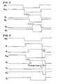
- Figure 4 shows RAS, the ⁇ pre signal, the first and second sensing signals ⁇ s1 and O s2 and the respective timing relationships of the signals in the conventional method for providing the sense and restore functions. It will be appreciated from a brief analysis of these waveforms that the sense and restore functions are always accomplished during the chip active period when the RAS signal is low.
- Figure 5 shows a series of waveforms illustrating the relative timing between the RAS signal, the 0p re signal, and the first and second sensing signals ⁇ s1 and O s2 and other signals generated in accordance with the invention.
- the second sensing signal is initiated after the chip active period has terminated and the precharge period has begun.
- the second sensing signal is generated independently of the first sensing signal and in fact will lag further behind the first sensing signal as the chip operates faster. This is a preferable method of completing the sense and restore functions with much less of an impact on the overall chip cycle time than would occur if the active period were extended to allow adequate completion of the sense and restore functions. This is especially true when midpoint sensing is utilized because the bit lines need only be shorted together to equilibrate them during the precharge period.
- the present invention has been described above in terms of one embodiment, but changes and modifications may be made.
- the invention is not limited to the provision only of two sensing signals, not to the application of signals to only two pairs of transistors.
- Other arrangements could be devised. There could be for instance, three or more pairs of transistors in the sense amplifier and a corresponding number of sensing signals. Some of the sensing signals may be functions of one another, while further sensing signals will be independent of other sensing signals. There could be plural transistor pairs in the sense amplifier with a lesser number of distinct sensing signals being distributed among them. Some of the sensing signals could be combined to form further sensing signals.
- the invention limited to generating the second or ultimate sensing signal in response to RAS going high. Other signals may be used or developed so that the interval between switching on transistors in the sense amplifier would not decrease, but preferably would increase, as the DRAM gets faster.
Landscapes
- Engineering & Computer Science (AREA)
- Microelectronics & Electronic Packaging (AREA)
- Computer Hardware Design (AREA)
- Physics & Mathematics (AREA)
- Electromagnetism (AREA)
- General Physics & Mathematics (AREA)
- Radar, Positioning & Navigation (AREA)
- Automation & Control Theory (AREA)
- Dram (AREA)
- Semiconductor Memories (AREA)
- Static Random-Access Memory (AREA)
Applications Claiming Priority (2)
| Application Number | Priority Date | Filing Date | Title |
|---|---|---|---|
| US672907 | 1984-11-19 | ||
| US06/672,907 US4656612A (en) | 1984-11-19 | 1984-11-19 | Dram current control technique |
Publications (3)
| Publication Number | Publication Date |
|---|---|
| EP0182457A2 true EP0182457A2 (fr) | 1986-05-28 |
| EP0182457A3 EP0182457A3 (en) | 1989-05-10 |
| EP0182457B1 EP0182457B1 (fr) | 1992-02-19 |
Family
ID=24700524
Family Applications (1)
| Application Number | Title | Priority Date | Filing Date |
|---|---|---|---|
| EP85305818A Expired - Lifetime EP0182457B1 (fr) | 1984-11-19 | 1985-08-15 | RAM dynamique, et méthode pour la stabilisation des impulsions de courant dans un tel circuit de mémoire |
Country Status (5)
| Country | Link |
|---|---|
| US (1) | US4656612A (fr) |
| EP (1) | EP0182457B1 (fr) |
| JP (1) | JPH07111827B2 (fr) |
| KR (1) | KR910002801B1 (fr) |
| DE (1) | DE3585402D1 (fr) |
Cited By (3)
| Publication number | Priority date | Publication date | Assignee | Title |
|---|---|---|---|---|
| DE3916972A1 (de) * | 1988-07-11 | 1990-01-18 | Samsung Electronics Co Ltd | Leseverstaerkertreiber fuer speichervorrichtung |
| EP0355828A3 (fr) * | 1988-08-26 | 1992-03-04 | Kabushiki Kaisha Toshiba | Circuit de commande pour une mémoire à semi-conducteurs et système de mémoire à semi-conducteurs |
| EP0452510A4 (en) * | 1989-11-07 | 1992-04-29 | Fujitsu Limited | Semiconductor memory device |
Families Citing this family (17)
| Publication number | Priority date | Publication date | Assignee | Title |
|---|---|---|---|---|
| US4825416A (en) * | 1986-05-07 | 1989-04-25 | Advanced Micro Devices, Inc. | Integrated electronic memory circuit with internal timing and operable in both latch-based and register-based systems |
| JPH06101227B2 (ja) * | 1986-11-29 | 1994-12-12 | 三菱電機株式会社 | 半導体メモリ装置 |
| JPH0812760B2 (ja) * | 1986-11-29 | 1996-02-07 | 三菱電機株式会社 | ダイナミックメモリ装置 |
| US4979190A (en) * | 1988-04-01 | 1990-12-18 | Digital Equipment Corporation | Method and apparatus for stabilized data transmission |
| JPH01263995A (ja) * | 1988-04-13 | 1989-10-20 | Nec Corp | ダイナミック型半導体記憶素子 |
| JP2534757B2 (ja) * | 1988-07-06 | 1996-09-18 | 株式会社東芝 | リフレッシュ回路 |
| US4985865A (en) * | 1988-12-21 | 1991-01-15 | Texas Instruments Incorporated | Asymmetrical delay for controlling word line selection |
| JP2614514B2 (ja) * | 1989-05-19 | 1997-05-28 | 三菱電機株式会社 | ダイナミック・ランダム・アクセス・メモリ |
| US5163168A (en) * | 1990-03-30 | 1992-11-10 | Matsushita Electric Industrial Co., Ltd. | Pulse signal generator and redundancy selection signal generator |
| EP0467638B1 (fr) * | 1990-07-17 | 1997-05-07 | Nec Corporation | Dispositif de mémoire à semi-conducteur |
| US5313422A (en) * | 1991-05-29 | 1994-05-17 | Texas Instruments Incorporated | Digitally controlled delay applied to address decoder for write vs. read |
| US5359630A (en) * | 1992-08-13 | 1994-10-25 | Digital Equipment Corporation | Method and apparatus for realignment of synchronous data |
| US6463396B1 (en) * | 1994-05-31 | 2002-10-08 | Kabushiki Kaisha Toshiba | Apparatus for controlling internal heat generating circuit |
| US5532969A (en) * | 1994-10-07 | 1996-07-02 | International Business Machines Corporation | Clocking circuit with increasing delay as supply voltage VDD |
| US5602785A (en) * | 1995-12-13 | 1997-02-11 | Micron Technology, Inc. | P-channel sense amplifier pull-up circuit with a timed pulse for use in DRAM memories having non-bootstrapped word lines |
| US6535798B1 (en) * | 1998-12-03 | 2003-03-18 | Intel Corporation | Thermal management in a system |
| KR100300079B1 (ko) * | 1999-07-28 | 2001-11-01 | 김영환 | 센스앰프 구동회로 |
Family Cites Families (12)
| Publication number | Priority date | Publication date | Assignee | Title |
|---|---|---|---|---|
| US3796998A (en) * | 1971-09-07 | 1974-03-12 | Texas Instruments Inc | Mos dynamic memory |
| US3996481A (en) * | 1974-11-19 | 1976-12-07 | International Business Machines Corporation | FET load gate compensator |
| US4081701A (en) * | 1976-06-01 | 1978-03-28 | Texas Instruments Incorporated | High speed sense amplifier for MOS random access memory |
| JPS5441633A (en) * | 1977-09-09 | 1979-04-03 | Hitachi Ltd | Readout system for memory cell |
| JPS54150064A (en) * | 1978-05-18 | 1979-11-24 | Toshiba Corp | Pulse generation circuit |
| JPS594790B2 (ja) * | 1978-05-18 | 1984-01-31 | 株式会社東芝 | メモリ−回路 |
| US4222112A (en) * | 1979-02-09 | 1980-09-09 | Bell Telephone Laboratories, Incorporated | Dynamic RAM organization for reducing peak current |
| DE3101520A1 (de) * | 1981-01-19 | 1982-08-26 | Siemens AG, 1000 Berlin und 8000 München | Monolithisch integrierter halbleiterspeicher |
| US4421996A (en) * | 1981-10-09 | 1983-12-20 | Advanced Micro Devices, Inc. | Sense amplification scheme for random access memory |
| JPS5987696A (ja) * | 1982-11-10 | 1984-05-21 | アドバンスト・マイクロ・デイバイシズ・インコ−ポレ−テツド | センス率の制御装置 |
| JPS5998390A (ja) * | 1982-11-26 | 1984-06-06 | Hitachi Ltd | ダイナミツク型mosram |
| US4551641A (en) * | 1983-11-23 | 1985-11-05 | Motorola, Inc. | Sense amplifier |
-
1984
- 1984-11-19 US US06/672,907 patent/US4656612A/en not_active Expired - Lifetime
-
1985
- 1985-08-15 DE DE8585305818T patent/DE3585402D1/de not_active Expired - Lifetime
- 1985-08-15 EP EP85305818A patent/EP0182457B1/fr not_active Expired - Lifetime
- 1985-10-09 JP JP60225937A patent/JPH07111827B2/ja not_active Expired - Fee Related
- 1985-10-18 KR KR1019850007685A patent/KR910002801B1/ko not_active Expired
Cited By (4)
| Publication number | Priority date | Publication date | Assignee | Title |
|---|---|---|---|---|
| DE3916972A1 (de) * | 1988-07-11 | 1990-01-18 | Samsung Electronics Co Ltd | Leseverstaerkertreiber fuer speichervorrichtung |
| EP0355828A3 (fr) * | 1988-08-26 | 1992-03-04 | Kabushiki Kaisha Toshiba | Circuit de commande pour une mémoire à semi-conducteurs et système de mémoire à semi-conducteurs |
| EP0452510A4 (en) * | 1989-11-07 | 1992-04-29 | Fujitsu Limited | Semiconductor memory device |
| US5335206A (en) * | 1989-11-07 | 1994-08-02 | Fujitsu Limited | Semiconductor storage device |
Also Published As
| Publication number | Publication date |
|---|---|
| JPS61126693A (ja) | 1986-06-14 |
| EP0182457B1 (fr) | 1992-02-19 |
| KR860004348A (ko) | 1986-06-20 |
| DE3585402D1 (de) | 1992-03-26 |
| JPH07111827B2 (ja) | 1995-11-29 |
| EP0182457A3 (en) | 1989-05-10 |
| US4656612A (en) | 1987-04-07 |
| KR910002801B1 (ko) | 1991-05-04 |
Similar Documents
| Publication | Publication Date | Title |
|---|---|---|
| EP0182457B1 (fr) | RAM dynamique, et méthode pour la stabilisation des impulsions de courant dans un tel circuit de mémoire | |
| US5673225A (en) | Word line voltage boosting circuit and method thereof | |
| US5995435A (en) | Semiconductor memory device having controllable supplying capability of internal voltage | |
| US5677649A (en) | Frequency-variable oscillator controlled high efficiency charge pump | |
| US5144585A (en) | Supply voltage converter for high-density semiconductor memory device | |
| US6043685A (en) | Circuit for controlling sense amplifier over-driving voltage | |
| US5268600A (en) | Boosting clamping circuit and output buffer circuit using the same | |
| US5901055A (en) | Internal boosted voltage generator of semiconductor memory device | |
| US3937983A (en) | Mos buffer circuit | |
| US5111078A (en) | Input circuit for logic circuit having node and operating method therefor | |
| US5334890A (en) | Sense amplifier clock driver | |
| US6255900B1 (en) | Rapid on chip voltage generation for low power integrated circuits | |
| US5420823A (en) | Semiconductor memory with improved power supply control circuit | |
| US4649289A (en) | Circuit for maintaining the potential of a node of a MOS dynamic circuit | |
| JP3449752B2 (ja) | 低スイッチングノイズ出力バッファ | |
| US5504715A (en) | Word line loading compensating circuit of semiconductor memory device | |
| US5798970A (en) | Memory device output buffer | |
| US5754075A (en) | Integrated circuits including power supply boosters and methods of operating same | |
| US4618786A (en) | Precharge circuit for enhancement mode memory circuits | |
| JPH0413796B2 (fr) | ||
| EP1151365B1 (fr) | Generation rapide de tension dans le microcircuit dans le cas de circuits integres courant faible | |
| KR100333239B1 (ko) | 부트스트랩회로 | |
| US5404325A (en) | Dynamic random access memory device with precharging unit preventing counter electrodes of storage capacitors from voltage fluctuation | |
| US6438645B1 (en) | Apparatus and structure for rapid enablement | |
| KR940004516B1 (ko) | 반도체 메모리의 고속 센싱장치 |
Legal Events
| Date | Code | Title | Description |
|---|---|---|---|
| PUAI | Public reference made under article 153(3) epc to a published international application that has entered the european phase |
Free format text: ORIGINAL CODE: 0009012 |
|
| AK | Designated contracting states |
Kind code of ref document: A2 Designated state(s): DE FR GB NL |
|
| PUAL | Search report despatched |
Free format text: ORIGINAL CODE: 0009013 |
|
| AK | Designated contracting states |
Kind code of ref document: A3 Designated state(s): DE FR GB NL |
|
| 17P | Request for examination filed |
Effective date: 19890605 |
|
| RAP1 | Party data changed (applicant data changed or rights of an application transferred) |
Owner name: THORN EMI NORTH AMERICA INC. |
|
| 17Q | First examination report despatched |
Effective date: 19900531 |
|
| GRAA | (expected) grant |
Free format text: ORIGINAL CODE: 0009210 |
|
| AK | Designated contracting states |
Kind code of ref document: B1 Designated state(s): DE FR GB NL |
|
| REF | Corresponds to: |
Ref document number: 3585402 Country of ref document: DE Date of ref document: 19920326 |
|
| ET | Fr: translation filed | ||
| PLBE | No opposition filed within time limit |
Free format text: ORIGINAL CODE: 0009261 |
|
| STAA | Information on the status of an ep patent application or granted ep patent |
Free format text: STATUS: NO OPPOSITION FILED WITHIN TIME LIMIT |
|
| 26N | No opposition filed | ||
| REG | Reference to a national code |
Ref country code: GB Ref legal event code: IF02 |
|
| PGFP | Annual fee paid to national office [announced via postgrant information from national office to epo] |
Ref country code: FR Payment date: 20020722 Year of fee payment: 18 |
|
| PGFP | Annual fee paid to national office [announced via postgrant information from national office to epo] |
Ref country code: GB Payment date: 20020725 Year of fee payment: 18 |
|
| PGFP | Annual fee paid to national office [announced via postgrant information from national office to epo] |
Ref country code: NL Payment date: 20020726 Year of fee payment: 18 |
|
| PGFP | Annual fee paid to national office [announced via postgrant information from national office to epo] |
Ref country code: DE Payment date: 20020916 Year of fee payment: 18 |
|
| PG25 | Lapsed in a contracting state [announced via postgrant information from national office to epo] |
Ref country code: GB Free format text: LAPSE BECAUSE OF NON-PAYMENT OF DUE FEES Effective date: 20030815 |
|
| PG25 | Lapsed in a contracting state [announced via postgrant information from national office to epo] |
Ref country code: NL Free format text: LAPSE BECAUSE OF NON-PAYMENT OF DUE FEES Effective date: 20040301 |
|
| PG25 | Lapsed in a contracting state [announced via postgrant information from national office to epo] |
Ref country code: DE Free format text: LAPSE BECAUSE OF NON-PAYMENT OF DUE FEES Effective date: 20040302 |
|
| GBPC | Gb: european patent ceased through non-payment of renewal fee |
Effective date: 20030815 |
|
| PG25 | Lapsed in a contracting state [announced via postgrant information from national office to epo] |
Ref country code: FR Free format text: LAPSE BECAUSE OF NON-PAYMENT OF DUE FEES Effective date: 20040430 |
|
| NLV4 | Nl: lapsed or anulled due to non-payment of the annual fee |
Effective date: 20040301 |
|
| REG | Reference to a national code |
Ref country code: FR Ref legal event code: ST |