EP0182587B1 - Photolack und Verfahren zur Herstellung einer integrierten Schaltung - Google Patents
Photolack und Verfahren zur Herstellung einer integrierten Schaltung Download PDFInfo
- Publication number
- EP0182587B1 EP0182587B1 EP19850308229 EP85308229A EP0182587B1 EP 0182587 B1 EP0182587 B1 EP 0182587B1 EP 19850308229 EP19850308229 EP 19850308229 EP 85308229 A EP85308229 A EP 85308229A EP 0182587 B1 EP0182587 B1 EP 0182587B1
- Authority
- EP
- European Patent Office
- Prior art keywords
- photoresist
- integrated circuit
- photoconductivity
- complexing agent
- photoresist layer
- Prior art date
- Legal status (The legal status is an assumption and is not a legal conclusion. Google has not performed a legal analysis and makes no representation as to the accuracy of the status listed.)
- Expired
Links
- 229920002120 photoresistant polymer Polymers 0.000 title claims description 52
- 238000000034 method Methods 0.000 title claims description 26
- 238000004519 manufacturing process Methods 0.000 title claims description 9
- 239000008139 complexing agent Substances 0.000 claims description 14
- 150000001412 amines Chemical class 0.000 claims description 10
- 238000000059 patterning Methods 0.000 claims description 9
- 230000007246 mechanism Effects 0.000 claims description 8
- 238000012545 processing Methods 0.000 claims description 6
- RHLWQEFHFQTKNT-UHFFFAOYSA-N (2z)-1-cyclooctyl-2-diazocyclooctane Chemical compound [N-]=[N+]=C1CCCCCCC1C1CCCCCCC1 RHLWQEFHFQTKNT-UHFFFAOYSA-N 0.000 claims description 5
- XXTZHYXQVWRADW-UHFFFAOYSA-N diazomethanone Chemical compound [N]N=C=O XXTZHYXQVWRADW-UHFFFAOYSA-N 0.000 claims description 4
- 206010034972 Photosensitivity reaction Diseases 0.000 claims description 2
- 230000036211 photosensitivity Effects 0.000 claims description 2
- 239000000543 intermediate Substances 0.000 description 9
- 239000002184 metal Substances 0.000 description 9
- 229910052751 metal Inorganic materials 0.000 description 9
- 238000001020 plasma etching Methods 0.000 description 9
- 238000005530 etching Methods 0.000 description 8
- 239000012212 insulator Substances 0.000 description 6
- 235000012431 wafers Nutrition 0.000 description 6
- 239000000463 material Substances 0.000 description 5
- 239000004065 semiconductor Substances 0.000 description 5
- 201000006824 bubonic plague Diseases 0.000 description 4
- 230000008020 evaporation Effects 0.000 description 4
- 238000001704 evaporation Methods 0.000 description 4
- 238000009413 insulation Methods 0.000 description 4
- 150000001875 compounds Chemical class 0.000 description 3
- 230000001747 exhibiting effect Effects 0.000 description 3
- 238000001465 metallisation Methods 0.000 description 3
- 239000002904 solvent Substances 0.000 description 3
- 238000010521 absorption reaction Methods 0.000 description 2
- 230000010354 integration Effects 0.000 description 2
- 150000002739 metals Chemical class 0.000 description 2
- 230000002411 adverse Effects 0.000 description 1
- 238000013019 agitation Methods 0.000 description 1
- 238000013459 approach Methods 0.000 description 1
- 230000000740 bleeding effect Effects 0.000 description 1
- 230000009918 complex formation Effects 0.000 description 1
- 230000007797 corrosion Effects 0.000 description 1
- 238000005260 corrosion Methods 0.000 description 1
- 238000011161 development Methods 0.000 description 1
- 239000006185 dispersion Substances 0.000 description 1
- 230000000694 effects Effects 0.000 description 1
- 238000010894 electron beam technology Methods 0.000 description 1
- 238000000609 electron-beam lithography Methods 0.000 description 1
- 230000008030 elimination Effects 0.000 description 1
- 238000003379 elimination reaction Methods 0.000 description 1
- 238000010438 heat treatment Methods 0.000 description 1
- 238000005286 illumination Methods 0.000 description 1
- 125000000468 ketone group Chemical group 0.000 description 1
- 238000010907 mechanical stirring Methods 0.000 description 1
- 230000003287 optical effect Effects 0.000 description 1
- 150000003141 primary amines Chemical class 0.000 description 1
- 239000000523 sample Substances 0.000 description 1
- 150000003335 secondary amines Chemical class 0.000 description 1
- 239000013049 sediment Substances 0.000 description 1
- 238000004544 sputter deposition Methods 0.000 description 1
- 239000000126 substance Substances 0.000 description 1
- 239000000758 substrate Substances 0.000 description 1
- 150000003512 tertiary amines Chemical group 0.000 description 1
- 238000012360 testing method Methods 0.000 description 1
- 238000012546 transfer Methods 0.000 description 1
Images
Classifications
-
- G—PHYSICS
- G03—PHOTOGRAPHY; CINEMATOGRAPHY; ANALOGOUS TECHNIQUES USING WAVES OTHER THAN OPTICAL WAVES; ELECTROGRAPHY; HOLOGRAPHY
- G03F—PHOTOMECHANICAL PRODUCTION OF TEXTURED OR PATTERNED SURFACES, e.g. FOR PRINTING, FOR PROCESSING OF SEMICONDUCTOR DEVICES; MATERIALS THEREFOR; ORIGINALS THEREFOR; APPARATUS SPECIALLY ADAPTED THEREFOR
- G03F7/00—Photomechanical, e.g. photolithographic, production of textured or patterned surfaces, e.g. printing surfaces; Materials therefor, e.g. comprising photoresists; Apparatus specially adapted therefor
- G03F7/004—Photosensitive materials
- G03F7/022—Quinonediazides
- G03F7/0226—Quinonediazides characterised by the non-macromolecular additives
-
- G—PHYSICS
- G03—PHOTOGRAPHY; CINEMATOGRAPHY; ANALOGOUS TECHNIQUES USING WAVES OTHER THAN OPTICAL WAVES; ELECTROGRAPHY; HOLOGRAPHY
- G03F—PHOTOMECHANICAL PRODUCTION OF TEXTURED OR PATTERNED SURFACES, e.g. FOR PRINTING, FOR PROCESSING OF SEMICONDUCTOR DEVICES; MATERIALS THEREFOR; ORIGINALS THEREFOR; APPARATUS SPECIALLY ADAPTED THEREFOR
- G03F7/00—Photomechanical, e.g. photolithographic, production of textured or patterned surfaces, e.g. printing surfaces; Materials therefor, e.g. comprising photoresists; Apparatus specially adapted therefor
- G03F7/004—Photosensitive materials
- G03F7/038—Macromolecular compounds which are rendered insoluble or differentially wettable
Definitions
- This invention relates to a process for manufacturing an integrated circuit by using a photoresist.
- Photoresists commonly used in semiconductor integrated circuit device fabrication are excellent insulators, and as such are very susceptible to charge buildup during high voltage processes such as reactive ion etching (RIE) or plasma etching.
- RIE reactive ion etching
- production of integrated circuits commonly involves numerous photoresist mask patterning steps to control etching of metal or semiconductor to precise patterns. Etching of metals is easy; etching of semiconductors is not difficult; but etching of insulators is very difficult. Rather than resorting to etching of insulators, it is common to convert the patterns to stencil masks and vapour deposit the insulator patterns through stencil masks. There is very little patterning of insulation by etching; stencilling is the common approach.
- RIE reactive ion etching
- plasma etching are examples of etching techniques appropriate to such insulation patterning.
- Such techniques require high voltages, often in vacuum, in environments which may damage integrated circuit process intermediates as a result of charge buildup on the surfaces of the integrated circuits. Such damage may be inchoate; actual failure or even testability may be months in the future.
- Failure mechanisms affected by charge buildup include "SiO bumps", “resistor blowout", and a corrosion known as "black death”. Charge buildup can also affect the accuracy of e-beam patterning of photoresist, by defocussing the beam in a manner analogous to that of a deflection plate in a cathode ray tube.
- Photoresists commonly used in semiconductor (and other) device fabrication are excellent insulators.
- Current practice involves use of photoresist in many patterning steps such as metal or insulator patterning by either lift-off or RIE/plasma etch subtractive patterning.
- Evaporation of metals is commonly done using e-beam evaporation or e-beam heating or a crucible containing source material.
- Plasma precleans are common where metal-metal contacts are important or for improved metal-metal, insulator-metal adhesion. Each of these processes may cause charge buildup on the resist. The charge may cause extensive damage to underlying material and/or circuits.
- EP-A 0 067 954 discloses a photoresist comprising a photoresistivity complexing agent and an amine photoconductivity complexing agent.
- the invention seeks to provide a process which avoids charge buildup during fabrication of integrated circuits using photoresists.
- the invention provides a process for manufacturing an integrated circuit comprising the steps of providing a photoresist layer on an integrated circuit process intermediate and subsequently treating the integrated circuit process intermediate, with photoresist layer, to a patterning process step by mounting it on an attachment mechanism for processing in an environment of significant electric potential; the method being characterised, according to the invention, by the photoresist comprising a diazo ketone photosensitivity complexing agent and an amine photoconductivity complexing agent of low ionisation potential and such that the photoconductivity and photosensivity peaks of the photoresist are at different wavelengths; and means connecting the photoresist layer to a drain electrode at a reference potential, for charges resulting from the environment of significant electric potential.
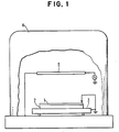
- a photoconductive photoresist 1 (shown greatly enlarged) on integrated circuit intermediate 2, is effective to bleed off charges to electrode 3 upon which the integrated circuit 2 is placed.
- the processing chamber 4 is equipped with another electrode 5 and such additional standard equipment as is required for its function.
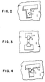
- Figures 2-4 illustrate failure mechanisms related to charge buildup.
- pattern 6 of metallisation over SiO insulation on intermediate 2 has SiO bumps 7 which interfere with mechanical strength and electrical conductivity.
- resistance material 8 has a discontinuity in its desired connection between areas of metallisation 9 on intermediate 2.
- FIG. 4 exhibiting "black death”, corroded dark patches 11 appear on metallisation 10 on intermediate 2.
- a common photoresist containing a diazoketone as the photoactive compound is compounded with a photoconductor by addition of an amine with low ionisation potential, diazobicyclooctane (DABCO).
- DABCO diazobicyclooctane
- Other amines with low ionisation potential include primary, secondary or tertiary amines
- This complex imparts conductive properties to the film in the presence of light.
- the photoresist retains its usual properties for exposure on normal tools used in the trade, but in the plasma discharge, RIE, e-beam evaporation or sputter deposition processes the photoconducting material conducts away the charge to the cathode through the normal means of wafer attachment. Charges may be dissipated via the semiconductor substrate to the electrode which is the source of reference potential (usually ground) for elimination of charge build-up. Depending upon the characteristics of the tool and of the integrated circuit intermediate, it may be advantageous to connect the photoconducting photoresist complex to ground by a conductive metal clip or probe.
- photoconducting photoresist in the processing, bleeding charges away through electrodes already present in the process, minimises failure mechanisms such as SiO bumps, resistor blowout and black death which are related to charge buildup.
- the photoconductivity exhibits no apparent undesirable side effects.
- the preferred photoconducting photoresist complex is prepared as follows:
- the process of using the photoconductive photoresist complex is as follows:
- the wavelength of absorption is determined by the difference between the ionisation potential of the amine and the electron affinity of the acceptor compound (diazoketone in the photoresist). This property allows the optimum wavelength for the photoconductivity to be tailored for particular light sources. This allows the photoresist to be conductive in a cleanroom/yellow light situation and thus gives protection against electrostatic damage to the devices. It also allows use where only a various band light source is permissible. Such a situation might be in an electron-beam exposure tool.
- any of the several available photoresists comprised in the definition of Claim 1 may be used as photoresist complexing agent, together with the amine photoconductivity complexing agent, for use as a photoconductive photoresist complex in accordance with the invention. So long as the photoconductivity complexing agent does not adversely react nor block light necessary for photoresist exposure, a range of photoconductive material may be substituted for that of the preferred embodiment.
Landscapes
- Physics & Mathematics (AREA)
- General Physics & Mathematics (AREA)
- Spectroscopy & Molecular Physics (AREA)
- Electron Beam Exposure (AREA)
- Drying Of Semiconductors (AREA)
- Photosensitive Polymer And Photoresist Processing (AREA)
Claims (3)
Applications Claiming Priority (2)
| Application Number | Priority Date | Filing Date | Title |
|---|---|---|---|
| US67230384A | 1984-11-16 | 1984-11-16 | |
| US672303 | 1984-11-16 |
Publications (3)
| Publication Number | Publication Date |
|---|---|
| EP0182587A2 EP0182587A2 (de) | 1986-05-28 |
| EP0182587A3 EP0182587A3 (en) | 1987-11-04 |
| EP0182587B1 true EP0182587B1 (de) | 1989-09-20 |
Family
ID=24697998
Family Applications (1)
| Application Number | Title | Priority Date | Filing Date |
|---|---|---|---|
| EP19850308229 Expired EP0182587B1 (de) | 1984-11-16 | 1985-11-12 | Photolack und Verfahren zur Herstellung einer integrierten Schaltung |
Country Status (3)
| Country | Link |
|---|---|
| EP (1) | EP0182587B1 (de) |
| JP (1) | JPS61125019A (de) |
| DE (1) | DE3573175D1 (de) |
Families Citing this family (2)
| Publication number | Priority date | Publication date | Assignee | Title |
|---|---|---|---|---|
| JPH083628B2 (ja) * | 1986-10-13 | 1996-01-17 | 三菱電機株式会社 | 非帯電性レジスト |
| US5168030A (en) * | 1986-10-13 | 1992-12-01 | Mitsubishi Denki Kabushiki Kaisha | Positive type o-quinone diazide photo-resist containing antistatic agent selected from hydrazones, ethylcarbazole and bis(dimethylamino)benzene |
Family Cites Families (10)
| Publication number | Priority date | Publication date | Assignee | Title |
|---|---|---|---|---|
| NL247939A (de) * | 1959-02-04 | |||
| FR2255629B1 (de) * | 1973-12-20 | 1976-10-22 | Ibm | |
| US4196003A (en) * | 1974-02-01 | 1980-04-01 | Fuji Photo Film Co., Ltd. | Light-sensitive o-quinone diazide copying composition |
| CA1120763A (en) * | 1977-11-23 | 1982-03-30 | James A. Carothers | Enhancement of resist development |
| DE3066410D1 (en) * | 1979-10-10 | 1984-03-08 | Ibm | Photo, e-beam, and x-ray sensitive negative resists based on donor polymer-doped halocarbon acceptor transfer complexes and method for producing negative resist images |
| CA1161685A (en) * | 1979-10-10 | 1984-02-07 | Ari Aviram | Class of x-ray resists based on donor polymer-doped halocarbon acceptor transfer complexes |
| JPS56125833A (en) * | 1980-03-07 | 1981-10-02 | Chiyou Lsi Gijutsu Kenkyu Kumiai | Exposing method for electron beam |
| JPS57170526A (en) * | 1981-04-14 | 1982-10-20 | Fujitsu Ltd | Exposing method and device for charged beam |
| JPS57188040A (en) * | 1981-05-15 | 1982-11-18 | Toshiba Corp | Electrophographic organic photoconductive composition |
| JPS59116745A (ja) * | 1982-12-24 | 1984-07-05 | Fujitsu Ltd | パタ−ン形成方法 |
-
1985
- 1985-07-18 JP JP15714885A patent/JPS61125019A/ja active Pending
- 1985-11-12 DE DE8585308229T patent/DE3573175D1/de not_active Expired
- 1985-11-12 EP EP19850308229 patent/EP0182587B1/de not_active Expired
Also Published As
| Publication number | Publication date |
|---|---|
| DE3573175D1 (en) | 1989-10-26 |
| EP0182587A2 (de) | 1986-05-28 |
| JPS61125019A (ja) | 1986-06-12 |
| EP0182587A3 (en) | 1987-11-04 |
Similar Documents
| Publication | Publication Date | Title |
|---|---|---|
| US4092442A (en) | Method of depositing thin films utilizing a polyimide mask | |
| US4600686A (en) | Method of forming a resist mask resistant to plasma etching | |
| US5169494A (en) | Fine pattern forming method | |
| CA1161787A (en) | Dry etching of copper patterns | |
| US20060154153A1 (en) | Anti-ESD photomask blank | |
| US4504574A (en) | Method of forming a resist mask resistant to plasma etching | |
| EP0083408B1 (de) | Verfahren und Vorrichtung zum Testen lithographischer Masken durch Abtastung mit einem Elektronenstrahl | |
| KR100293975B1 (ko) | 건식 에칭 방법 및 건식 에칭 방법을 이용한 반도체 장치의 제조방법 | |
| US6803156B2 (en) | Electrostatic damage (ESD) protected photomask | |
| US3346385A (en) | Process for photo-engraving by use of photo-chromic dye and product | |
| US6110624A (en) | Multiple polarity mask exposure method | |
| US4702993A (en) | Treatment of planarizing layer in multilayer electron beam resist | |
| US20010044077A1 (en) | Stabilization of chemically amplified resist coating | |
| EP0182587A2 (de) | Photolack und Verfahren zur Herstellung einer integrierten Schaltung | |
| US6632115B1 (en) | Method for forming transparent conductive film using chemically amplified resist | |
| US4968582A (en) | Photoresists resistant to oxygen plasmas | |
| EP0390038B1 (de) | Feinmusterherstellungsverfahren | |
| US5114827A (en) | Photoresists resistant to oxygen plasmas | |
| US4237208A (en) | Silane electron beam resists | |
| US4810617A (en) | Treatment of planarizing layer in multilayer electron beam resist | |
| JPS5993441A (ja) | レジスト | |
| US7252911B2 (en) | ESD-resistant photomask and method of preventing mask ESD damage | |
| US4595649A (en) | Glassy TiO2 polymer films as electron beam charge dissipation layers | |
| US4497884A (en) | Method for the production of a self-supporting mask | |
| JP2516968B2 (ja) | 二層構造電子線レジスト用平坦化材料 |
Legal Events
| Date | Code | Title | Description |
|---|---|---|---|
| PUAI | Public reference made under article 153(3) epc to a published international application that has entered the european phase |
Free format text: ORIGINAL CODE: 0009012 |
|
| AK | Designated contracting states |
Kind code of ref document: A2 Designated state(s): DE FR GB |
|
| 17P | Request for examination filed |
Effective date: 19860919 |
|
| PUAL | Search report despatched |
Free format text: ORIGINAL CODE: 0009013 |
|
| AK | Designated contracting states |
Kind code of ref document: A3 Designated state(s): DE FR GB |
|
| 17Q | First examination report despatched |
Effective date: 19880314 |
|
| GRAA | (expected) grant |
Free format text: ORIGINAL CODE: 0009210 |
|
| AK | Designated contracting states |
Kind code of ref document: B1 Designated state(s): DE FR GB |
|
| ET | Fr: translation filed | ||
| REF | Corresponds to: |
Ref document number: 3573175 Country of ref document: DE Date of ref document: 19891026 |
|
| PLBE | No opposition filed within time limit |
Free format text: ORIGINAL CODE: 0009261 |
|
| STAA | Information on the status of an ep patent application or granted ep patent |
Free format text: STATUS: NO OPPOSITION FILED WITHIN TIME LIMIT |
|
| 26N | No opposition filed | ||
| PGFP | Annual fee paid to national office [announced via postgrant information from national office to epo] |
Ref country code: GB Payment date: 19911008 Year of fee payment: 7 |
|
| PGFP | Annual fee paid to national office [announced via postgrant information from national office to epo] |
Ref country code: FR Payment date: 19911028 Year of fee payment: 7 |
|
| PGFP | Annual fee paid to national office [announced via postgrant information from national office to epo] |
Ref country code: DE Payment date: 19911118 Year of fee payment: 7 |
|
| PGFP | Annual fee paid to national office [announced via postgrant information from national office to epo] |
Ref country code: LU Payment date: 19921027 Year of fee payment: 8 |
|
| PG25 | Lapsed in a contracting state [announced via postgrant information from national office to epo] |
Ref country code: GB Effective date: 19921112 |
|
| EPTA | Lu: last paid annual fee | ||
| GBPC | Gb: european patent ceased through non-payment of renewal fee |
Effective date: 19921112 |
|
| PG25 | Lapsed in a contracting state [announced via postgrant information from national office to epo] |
Ref country code: FR Effective date: 19930730 |
|
| PG25 | Lapsed in a contracting state [announced via postgrant information from national office to epo] |
Ref country code: DE Effective date: 19930803 |
|
| REG | Reference to a national code |
Ref country code: FR Ref legal event code: ST |