EP0182610A2 - Halbleiter-Fotodetektorvorrichtung - Google Patents
Halbleiter-Fotodetektorvorrichtung Download PDFInfo
- Publication number
- EP0182610A2 EP0182610A2 EP85308283A EP85308283A EP0182610A2 EP 0182610 A2 EP0182610 A2 EP 0182610A2 EP 85308283 A EP85308283 A EP 85308283A EP 85308283 A EP85308283 A EP 85308283A EP 0182610 A2 EP0182610 A2 EP 0182610A2
- Authority
- EP
- European Patent Office
- Prior art keywords
- gate
- gate electrode
- junction
- extension portion
- photodetector device
- Prior art date
- Legal status (The legal status is an assumption and is not a legal conclusion. Google has not performed a legal analysis and makes no representation as to the accuracy of the status listed.)
- Granted
Links
Images


Classifications
-
- H—ELECTRICITY
- H10—SEMICONDUCTOR DEVICES; ELECTRIC SOLID-STATE DEVICES NOT OTHERWISE PROVIDED FOR
- H10F—INORGANIC SEMICONDUCTOR DEVICES SENSITIVE TO INFRARED RADIATION, LIGHT, ELECTROMAGNETIC RADIATION OF SHORTER WAVELENGTH OR CORPUSCULAR RADIATION
- H10F30/00—Individual radiation-sensitive semiconductor devices in which radiation controls the flow of current through the devices, e.g. photodetectors
- H10F30/20—Individual radiation-sensitive semiconductor devices in which radiation controls the flow of current through the devices, e.g. photodetectors the devices having potential barriers, e.g. phototransistors
- H10F30/21—Individual radiation-sensitive semiconductor devices in which radiation controls the flow of current through the devices, e.g. photodetectors the devices having potential barriers, e.g. phototransistors the devices being sensitive to infrared, visible or ultraviolet radiation
- H10F30/28—Individual radiation-sensitive semiconductor devices in which radiation controls the flow of current through the devices, e.g. photodetectors the devices having potential barriers, e.g. phototransistors the devices being sensitive to infrared, visible or ultraviolet radiation the devices being characterised by field-effect operation, e.g. junction field-effect phototransistors
- H10F30/282—Insulated-gate field-effect transistors [IGFET], e.g. MISFET [metal-insulator-semiconductor field-effect transistor] phototransistors
-
- H—ELECTRICITY
- H10—SEMICONDUCTOR DEVICES; ELECTRIC SOLID-STATE DEVICES NOT OTHERWISE PROVIDED FOR
- H10F—INORGANIC SEMICONDUCTOR DEVICES SENSITIVE TO INFRARED RADIATION, LIGHT, ELECTROMAGNETIC RADIATION OF SHORTER WAVELENGTH OR CORPUSCULAR RADIATION
- H10F77/00—Constructional details of devices covered by this subclass
- H10F77/10—Semiconductor bodies
- H10F77/16—Material structures, e.g. crystalline structures, film structures or crystal plane orientations
-
- Y—GENERAL TAGGING OF NEW TECHNOLOGICAL DEVELOPMENTS; GENERAL TAGGING OF CROSS-SECTIONAL TECHNOLOGIES SPANNING OVER SEVERAL SECTIONS OF THE IPC; TECHNICAL SUBJECTS COVERED BY FORMER USPC CROSS-REFERENCE ART COLLECTIONS [XRACs] AND DIGESTS
- Y02—TECHNOLOGIES OR APPLICATIONS FOR MITIGATION OR ADAPTATION AGAINST CLIMATE CHANGE
- Y02E—REDUCTION OF GREENHOUSE GAS [GHG] EMISSIONS, RELATED TO ENERGY GENERATION, TRANSMISSION OR DISTRIBUTION
- Y02E10/00—Energy generation through renewable energy sources
- Y02E10/50—Photovoltaic [PV] energy
- Y02E10/547—Monocrystalline silicon PV cells
Definitions
- the invention relates to a photodetector, more but not necessarily exclusively, particularly/, to semiconductor photodetector devices serving as image elements of a solid state imaging device.
- Various devices such as a bipolar transistor type device, an insulating gate field effect transistor (FET), and a charge coupled device (CCD) are used as. semiconductor photodetector devices in solid state imaging devices. All of the above-mentioned devices have a P-type (or N-type) silicon substrate and an N-type (or P-type) region therein so as to form a PN junction, and utilize the photovoltaic-effect brought about by illuminating the PN junction region with light.
- a light receiving structure basically corresponds to a P-N junction photodiode.
- the P-N junction photodiode in which a P-type silicon substrate is grounded and a N-type region formed in the substrate is at a positive potential, i.e., the PN junction is reverse-biased, the energy of the light photons creates electron-hole pairs in a depletion region, creates electrons in the P-type substrate, and creates holes in the N-type region.
- the electron-hole pairs are separated by the electric field, leading to a current flow in an external circuit as carriers drift across the depletion region.
- the total current (photo-current) of the P-N photodiode is the drift current due to carriers.generated in the depletion region and the diffusion current due to carriers generated in the P-type substrate and the N-type region and diffusing into the PN junction.
- Such a PN junction photodiode carries with it the following disadvantages.
- An / of the present invention may provide a semiconductor photodetector device in which the above-mentioned disadvantages may be alleviated.
- a semiconductor photodetector device comprising an insulating gate field effect transistor (FET) having a channel region of a first conductivity type, a gate electrode of a second conductivity type, opposite to the first conductivity type, and a gate extension portion of the first conductivity type, the gate electrode and the gate extension portion forming a PN junction outside the channel region and an area including the PN junction receiving a light.
- FET insulating gate field effect transistor
- the gate electrode and gate extension portion are made of single crystalline silicon.
- the photodetection process in the photodetector an embodiment of device according to/the present invention is performed in the following manner.
- the PN junction is reverse biased and the joining area including the PN junction illuminated by light.
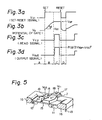
- An electric charge generated in a depletion region formed at the PN junction is accumulated in the gate electrode of doped single crystalline or polycrystalline silicon, so that the FET is an "on" state.
- a read signal e.g., pulse signal
- an output signal from a source region of the FET is detected and the light intensity can be measured since the current density of the output signal is related to the light intensity.
- the PN junction is forward biased to remove the charge accumulated in the gate electrode, and thus the photodetector element is reset.
- the electric charge in the gate electrode can be removed (escaped) through the gate extension portion, so that lag or persistence can be decreased.
- the P-type silicon substrate 13 is grounded, and the drain region 11 is connected to a d.c. supply E of, e.g., +5 V, through an FET Q, which is made "on” by applying a read signal VC2.
- the source region 12 is connected to a load resistance R and an output signal V out from the source region 12 is obtained.
- the gate extension portion 17 of N +- type single crystalline silicon is connected to a suitable device (not shown) sending a control signal V C1 of, e.g., +5 V, for setting and resetting the photodetector device. ( e .g. OV)
- the potential of the control signal V C1 is returned to "0" for a period D, whereby the charge accumulated in the gate electrode 14 is removed through the gate extension portion 17.
- the photodetector device is reset to an initial state.
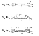
- a resist pattern 20 is formed on the P +- type silicon layer SS by a conventional method.
- the P + -type silicon layer SS is selectively etched by a suitable etching method, e.g., a reactive ion etching (RIE) method, to form a gate electrode and a gate extension portion.
- RIE reactive ion etching
- arsenic ions (As+) are implanted into the P-type silicon substrate 13 by an ion-implantation method to form the N +- type drain region 11 and the N +- type source region 12.
- the conditions of the ion-implantation treatment are, e.g., an accelerated energy of 100 keV and a dosage of approximately 5 x 10 15 cm- 2 .
- the resist pattern 20 is then removed.
- another resist pattern 21 is formed on the exposed surface except for at least the gate extension portion 17.
- phosphorus ions P + are implanted into the gate extension portion 17 of the P + -type silicon to convert it to an N +- type conductivity type.
- the conditions of the ion-implantation treatment are, e.g., an accelerated energy of 80 keV and a dosage of approxi- m ately 5 x 10 15 cm- 2 .
- the resist pattern 21 is then removed. Thereafter an annealing treatment is carried out at a temperature of, e.g., approximately 1000°C, for a period of, e.g., 30 minutes.
- a P-type region between the P -type gate electrode and the N +- type gate extension portion by doping a low impurity concentration of acceptors into a portion of the single crystalline silicon layer SS.
- an ion-implantation treatment for the P-type region is carried out at a dosage 1 to 5 x 10 a 13 cm -2 , lower than for the P +- type gate electrode.
- Such/P-type region can increase the sensitivity of the photodetector device.
- the photodetector device In the photodetector device according to/the present invention, electric charges generated by light are accumulated and then a signal of the accumulated charges is amplified by an FET for detection. Therefore, the sensitivity to faint light can be increased.
- a floating (parasitic) capacitance of the gate electrode can be reduced to a very small value, so that a high sensitivity is maintained.
- the light receiving area is defined on a single crystalline silicon portion formed on an insulating layer, so that the area is completely isolated from other light receiving areas of other photodetector devices.
- the potential of the gate electrode storing electric charges resets to "0" directly after the detection, so that lag (persistence) can be prevented. Therefore be photodetector devices of the present invention can/used for a solid state imaging device, whereby the accuracy and reliability of the image processing are increased.
Landscapes
- Solid State Image Pick-Up Elements (AREA)
- Light Receiving Elements (AREA)
- Transforming Light Signals Into Electric Signals (AREA)
Applications Claiming Priority (2)
| Application Number | Priority Date | Filing Date | Title |
|---|---|---|---|
| JP59241978A JPS61120466A (ja) | 1984-11-16 | 1984-11-16 | 半導体光検出素子 |
| JP241978/84 | 1984-11-16 |
Publications (3)
| Publication Number | Publication Date |
|---|---|
| EP0182610A2 true EP0182610A2 (de) | 1986-05-28 |
| EP0182610A3 EP0182610A3 (en) | 1986-09-17 |
| EP0182610B1 EP0182610B1 (de) | 1990-01-17 |
Family
ID=17082418
Family Applications (1)
| Application Number | Title | Priority Date | Filing Date |
|---|---|---|---|
| EP85308283A Expired - Lifetime EP0182610B1 (de) | 1984-11-16 | 1985-11-14 | Halbleiter-Fotodetektorvorrichtung |
Country Status (5)
| Country | Link |
|---|---|
| US (1) | US4841349A (de) |
| EP (1) | EP0182610B1 (de) |
| JP (1) | JPS61120466A (de) |
| KR (1) | KR890004476B1 (de) |
| DE (1) | DE3575498D1 (de) |
Cited By (2)
| Publication number | Priority date | Publication date | Assignee | Title |
|---|---|---|---|---|
| US5021849A (en) * | 1989-10-30 | 1991-06-04 | Motorola, Inc. | Compact SRAM cell with polycrystalline silicon diode load |
| USRE37769E1 (en) | 1990-04-30 | 2002-06-25 | Stmicroelectronics, Inc. | Methods for fabricating memory cells and load elements |
Families Citing this family (25)
| Publication number | Priority date | Publication date | Assignee | Title |
|---|---|---|---|---|
| JP2857397B2 (ja) * | 1988-08-05 | 1999-02-17 | シャープ株式会社 | 光駆動型半導体装置の製造方法 |
| US5241575A (en) * | 1989-12-21 | 1993-08-31 | Minolta Camera Kabushiki Kaisha | Solid-state image sensing device providing a logarithmically proportional output signal |
| IL96623A0 (en) * | 1989-12-26 | 1991-09-16 | Gen Electric | Low capacitance,large area semiconductor photodetector and photodetector system |
| US5117113A (en) * | 1990-07-06 | 1992-05-26 | Thompson And Nielson Electronics Ltd. | Direct reading dosimeter |
| US6013565A (en) * | 1991-12-16 | 2000-01-11 | Penn State Research Foundation | High conductivity thin film material for semiconductor device |
| JPH05219443A (ja) * | 1992-02-05 | 1993-08-27 | Minolta Camera Co Ltd | 固体撮像装置 |
| US5557114A (en) * | 1995-01-12 | 1996-09-17 | International Business Machines Corporation | Optical fet |
| US6144366A (en) * | 1996-10-18 | 2000-11-07 | Kabushiki Kaisha Toshiba | Method and apparatus for generating information input using reflected light image of target object |
| US6746893B1 (en) | 1997-07-29 | 2004-06-08 | Micron Technology, Inc. | Transistor with variable electron affinity gate and methods of fabrication and use |
| US7154153B1 (en) | 1997-07-29 | 2006-12-26 | Micron Technology, Inc. | Memory device |
| US6965123B1 (en) | 1997-07-29 | 2005-11-15 | Micron Technology, Inc. | Transistor with variable electron affinity gate and methods of fabrication and use |
| US7196929B1 (en) | 1997-07-29 | 2007-03-27 | Micron Technology Inc | Method for operating a memory device having an amorphous silicon carbide gate insulator |
| US6794255B1 (en) | 1997-07-29 | 2004-09-21 | Micron Technology, Inc. | Carburized silicon gate insulators for integrated circuits |
| US6936849B1 (en) * | 1997-07-29 | 2005-08-30 | Micron Technology, Inc. | Silicon carbide gate transistor |
| US6031263A (en) | 1997-07-29 | 2000-02-29 | Micron Technology, Inc. | DEAPROM and transistor with gallium nitride or gallium aluminum nitride gate |
| US6046466A (en) * | 1997-09-12 | 2000-04-04 | Nikon Corporation | Solid-state imaging device |
| JPH11274466A (ja) | 1998-03-20 | 1999-10-08 | Nikon Corp | 固体撮像装置及びこれを備えたカメラ |
| US6545333B1 (en) | 2001-04-25 | 2003-04-08 | International Business Machines Corporation | Light controlled silicon on insulator device |
| US6936895B2 (en) * | 2003-10-09 | 2005-08-30 | Chartered Semiconductor Manufacturing Ltd. | ESD protection device |
| US8477125B2 (en) * | 2005-12-21 | 2013-07-02 | Samsung Display Co., Ltd. | Photo sensor and organic light-emitting display using the same |
| US8476709B2 (en) | 2006-08-24 | 2013-07-02 | Infineon Technologies Ag | ESD protection device and method |
| JP2008288499A (ja) * | 2007-05-21 | 2008-11-27 | Panasonic Corp | 半導体装置及びその製造方法 |
| JP5196963B2 (ja) * | 2007-11-09 | 2013-05-15 | 株式会社ジャパンディスプレイウェスト | 表示装置および表示制御方法ならびに電子機器 |
| US9070784B2 (en) | 2011-07-22 | 2015-06-30 | Taiwan Semiconductor Manufacturing Company, Ltd. | Metal gate structure of a CMOS semiconductor device and method of forming the same |
| CN109920895B (zh) * | 2019-03-12 | 2024-02-09 | 中国科学院微电子研究所 | 可控发光位置的二极管器件、制造方法、电压控制方法 |
Family Cites Families (12)
| Publication number | Priority date | Publication date | Assignee | Title |
|---|---|---|---|---|
| US3207926A (en) * | 1962-07-06 | 1965-09-21 | Bell Telephone Labor Inc | Stabilized timing network |
| GB1139170A (en) * | 1965-12-22 | 1969-01-08 | Mullard Ltd | Thin film transistors |
| US3459944A (en) * | 1966-01-04 | 1969-08-05 | Ibm | Photosensitive insulated gate field effect transistor |
| US3648258A (en) * | 1969-07-01 | 1972-03-07 | Sperry Rand Corp | Optical memory circuit |
| US4057819A (en) * | 1976-08-05 | 1977-11-08 | Alan Ernest Owen | Semiconductor device |
| US4099196A (en) * | 1977-06-29 | 1978-07-04 | Intel Corporation | Triple layer polysilicon cell |
| JPS5850030B2 (ja) * | 1979-03-08 | 1983-11-08 | 日本放送協会 | 光電変換装置およびそれを用いた固体撮像板 |
| JPS55156371A (en) * | 1979-05-24 | 1980-12-05 | Toshiba Corp | Non-volatile semiconductor memory device |
| US4236831A (en) * | 1979-07-27 | 1980-12-02 | Honeywell Inc. | Semiconductor apparatus |
| US4419586A (en) * | 1981-08-27 | 1983-12-06 | Motorola, Inc. | Solid-state relay and regulator |
| JPS5922360A (ja) * | 1982-07-28 | 1984-02-04 | Matsushita Electric Works Ltd | 光入力モス型トランジスタ |
| US4564770A (en) * | 1983-03-29 | 1986-01-14 | Rca Corporation | Solid state relay with fast turnoff |
-
1984
- 1984-11-16 JP JP59241978A patent/JPS61120466A/ja active Pending
-
1985
- 1985-11-14 EP EP85308283A patent/EP0182610B1/de not_active Expired - Lifetime
- 1985-11-14 DE DE8585308283T patent/DE3575498D1/de not_active Expired - Lifetime
- 1985-11-15 KR KR1019850008542A patent/KR890004476B1/ko not_active Expired
-
1987
- 1987-10-28 US US07/113,324 patent/US4841349A/en not_active Expired - Fee Related
Cited By (2)
| Publication number | Priority date | Publication date | Assignee | Title |
|---|---|---|---|---|
| US5021849A (en) * | 1989-10-30 | 1991-06-04 | Motorola, Inc. | Compact SRAM cell with polycrystalline silicon diode load |
| USRE37769E1 (en) | 1990-04-30 | 2002-06-25 | Stmicroelectronics, Inc. | Methods for fabricating memory cells and load elements |
Also Published As
| Publication number | Publication date |
|---|---|
| KR860004479A (ko) | 1986-06-23 |
| JPS61120466A (ja) | 1986-06-07 |
| EP0182610B1 (de) | 1990-01-17 |
| EP0182610A3 (en) | 1986-09-17 |
| DE3575498D1 (de) | 1990-02-22 |
| US4841349A (en) | 1989-06-20 |
| KR890004476B1 (ko) | 1989-11-04 |
Similar Documents
| Publication | Publication Date | Title |
|---|---|---|
| EP0182610B1 (de) | Halbleiter-Fotodetektorvorrichtung | |
| US4916512A (en) | Photoelectric converter | |
| US6858912B2 (en) | Photodetector circuit | |
| US6111300A (en) | Multiple color detection elevated pin photo diode active pixel sensor | |
| US5043783A (en) | Solid state image sensor | |
| JP4131031B2 (ja) | 受光素子を有する半導体装置、光学ピックアップ装置、および受光素子を有する半導体装置の製造方法 | |
| KR100253820B1 (ko) | 포토디텍터 및 그의 제조방법 | |
| EP0625803A1 (de) | Photodiodenstruktur | |
| JPH06500431A (ja) | フォトダイオードとccdエレメントとの間に転送ゲートを有するイメージセンサ | |
| EP0544260A1 (de) | Überlaufvorrichtung für einen CCD-Bildsensor | |
| US4589003A (en) | Solid state image sensor comprising photoelectric converting film and reading-out transistor | |
| US5118631A (en) | Self-aligned antiblooming structure for charge-coupled devices and method of fabrication thereof | |
| US4906856A (en) | Semiconductive photodetection device having coplanar circuit components | |
| US4499654A (en) | Method for fabricating semiconductor photodetector | |
| EP0118568B1 (de) | Halbleiter-bildaufzeichnungsvorrichtung | |
| EP0015596B1 (de) | Ladungsgekoppelte Vorrichtungen | |
| US4603342A (en) | Imaging array having higher sensitivity and a method of making the same | |
| Elliott | Cadmium mercury telluride infrared detectors | |
| US4967249A (en) | Gain compression photodetector array | |
| JPH0570946B2 (de) | ||
| JPS61141176A (ja) | 半導体光検出装置 | |
| RU2781461C1 (ru) | Способ изготовления фотоприемника | |
| KR0147603B1 (ko) | 고체촬상소자 및 그 제조방법 | |
| US4658497A (en) | Method of making an imaging array having a higher sensitivity | |
| JPH09232617A (ja) | 赤外線検知素子及びその製造方法 |
Legal Events
| Date | Code | Title | Description |
|---|---|---|---|
| PUAI | Public reference made under article 153(3) epc to a published international application that has entered the european phase |
Free format text: ORIGINAL CODE: 0009012 |
|
| AK | Designated contracting states |
Kind code of ref document: A2 Designated state(s): DE FR GB |
|
| PUAL | Search report despatched |
Free format text: ORIGINAL CODE: 0009013 |
|
| AK | Designated contracting states |
Kind code of ref document: A3 Designated state(s): DE FR GB |
|
| 17P | Request for examination filed |
Effective date: 19870303 |
|
| 17Q | First examination report despatched |
Effective date: 19890503 |
|
| GRAA | (expected) grant |
Free format text: ORIGINAL CODE: 0009210 |
|
| AK | Designated contracting states |
Kind code of ref document: B1 Designated state(s): DE FR GB |
|
| REF | Corresponds to: |
Ref document number: 3575498 Country of ref document: DE Date of ref document: 19900222 |
|
| ET | Fr: translation filed | ||
| PLBE | No opposition filed within time limit |
Free format text: ORIGINAL CODE: 0009261 |
|
| STAA | Information on the status of an ep patent application or granted ep patent |
Free format text: STATUS: NO OPPOSITION FILED WITHIN TIME LIMIT |
|
| 26N | No opposition filed | ||
| PGFP | Annual fee paid to national office [announced via postgrant information from national office to epo] |
Ref country code: GB Payment date: 19920903 Year of fee payment: 8 |
|
| PGFP | Annual fee paid to national office [announced via postgrant information from national office to epo] |
Ref country code: FR Payment date: 19921127 Year of fee payment: 8 |
|
| PGFP | Annual fee paid to national office [announced via postgrant information from national office to epo] |
Ref country code: DE Payment date: 19930129 Year of fee payment: 8 |
|
| PG25 | Lapsed in a contracting state [announced via postgrant information from national office to epo] |
Ref country code: GB Effective date: 19931114 |
|
| GBPC | Gb: european patent ceased through non-payment of renewal fee |
Effective date: 19931114 |
|
| PG25 | Lapsed in a contracting state [announced via postgrant information from national office to epo] |
Ref country code: FR Effective date: 19940729 |
|
| PG25 | Lapsed in a contracting state [announced via postgrant information from national office to epo] |
Ref country code: DE Effective date: 19940802 |
|
| REG | Reference to a national code |
Ref country code: FR Ref legal event code: ST |