EP0183260A2 - Schrittmotorantriebsschaltung - Google Patents
Schrittmotorantriebsschaltung Download PDFInfo
- Publication number
- EP0183260A2 EP0183260A2 EP85115094A EP85115094A EP0183260A2 EP 0183260 A2 EP0183260 A2 EP 0183260A2 EP 85115094 A EP85115094 A EP 85115094A EP 85115094 A EP85115094 A EP 85115094A EP 0183260 A2 EP0183260 A2 EP 0183260A2
- Authority
- EP
- European Patent Office
- Prior art keywords
- transistor
- excitation
- power source
- drive circuit
- excitation coils
- Prior art date
- Legal status (The legal status is an assumption and is not a legal conclusion. Google has not performed a legal analysis and makes no representation as to the accuracy of the status listed.)
- Granted
Links
Images


Classifications
-
- H—ELECTRICITY
- H02—GENERATION; CONVERSION OR DISTRIBUTION OF ELECTRIC POWER
- H02P—CONTROL OR REGULATION OF ELECTRIC MOTORS, ELECTRIC GENERATORS OR DYNAMO-ELECTRIC CONVERTERS; CONTROLLING TRANSFORMERS, REACTORS OR CHOKE COILS
- H02P8/00—Arrangements for controlling dynamo-electric motors rotating step by step
- H02P8/12—Control or stabilisation of current
Definitions
- the present invention relates to a stepping motor drive circuit.
- circuits for driving a stepping motor which is rotated and driven in response to an excitation phase switching signal or a step pulse signal supplied from an external control section there are circuits for driving a stepping motor which is rotated and driven in response to an excitation phase switching signal or a step pulse signal supplied from an external control section.
- a switching device such as a transistor or the like which is turned on or off by the excitation phase switching signal is inserted in each excitation voltage supply path of each excitation coil constituting each excitation phase of the stepping motor, and when a level of the excitation phase switching signal is changed to switch the excitation phase, an excitation current flows through a corresponding excitation coil from a power source.
- this excitation current value does not immediately become a specified value after the conduction of the switching transistor but increases in accordance with a characteristic curve which is determined by a time constant of the inductance and resistance value.
- some of the constant current control circuits are constituted such that a large current flows at the start of conduction of the switching transistor using a current amplifying transistor and after an elapse of a constant period of time, the current is reduced and thereafter it is suppressed to a constant value.
- the stepping motor drive circuit having such a constant current control circuit still has the following problems which must be solved. Namely, in the constant current control circuit, the current amplifying transistor is operated to suppress the current value a constant period of time after the current starts to rise, resulting in an increase in generation of heat due to the collector dissipation. Therefore, it is required to arrange devices and design a heat radiation mechanism in consideration of heat radiation due to the operation for a long time. On the other hand, a service life of a device could be reduced due to the heat generation as well.
- a stepping motor drive circuit comprising: a plurality of switching transistors, respectively connected between a reference potential terminal and first ends of a plurality of excitation coils, for controlling currents flowing through these excitation coils; and a constant current control circuit, connected between a power source terminal and a second end of each of the plurality of excitation coils, for setting the currents flowing through the plurality of excitation coils to a constant value, wherein this constant current control circuit includes first and second resistors, a first transistor whose current path is connected at one end to the power source terminal through the first resistor and connected at the other end to each of the other ends of the plurality of excitation coils, a control circuit whose control terminal is connected to one end of the current path of the first transistor through the second resistor and which supplies a control signal to a base of the first transistor in response to a voltage drop in the first resistor thereby to control the conduction state of the first transistor, and a feedback circuit having a predetermined time constant and connected between the control terminal
- the feed-back circuit having a predetermined time constant since the feed-back circuit having a predetermined time constant is used, when the first transistor is made nonconductive, the voltage across the first resistor is not immediately set at a value nearly equal to 0V but gradually changes towards Ov in accordance with the time constant of the feedback circuit. Therefore, the first transistor is held in the nonconductive state for a predetermined period of time, thereby reducing the mean value of the current flowing through the excitation coil.
- Terminals A, B, A, and B of excitation coils 2A to 2D are connected to power source terminal VC through flywheel diodes 8A to 8D and a Zener diode 9 for suppressing a surge voltage, respectively.
- Control circuit 4 has a current detecting resistor 10 which is connected at one end to power source terminal VC and a current controlling pnp transistor 11 whose emitter is connected to the other end of resistor 10.
- a collector of transistor 11 is connected to common terminal COM of excitation coils 2A to 2D.
- An emitter of a pnp transistor 12 to control the conduction state of transistor 11 is connected to power source terminal VC.
- a base of transistor 12 is connected to the emitter of transistor 11 through a current limiting resistor 13.
- a collector of transistor 12 is connected to a base of transistor 11 and also grounded through a resistor 14.
- a feedback circuit having a series circuit of a resistor 15 and a capacitor 16 is connected between the base of transistor 12 and the collector of transistor 11.
- a flywheel diode 17 is interposed between the collector of transistor 11 and the ground.
- a diode 18 is interposed between the collector of transistor 11 and power source terminal VC.
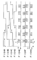
- step pulse signals SA to SD having the same period (pulse width TO) are ordinarily generated from output terminals ECA to ECD of control circuit 7 such that their phases are shifted by 1/4 of the period at a time.
- step pulse signals SA of phase "A" changes from a low level to a high level at time t 0 .
- switching transistor 6A is made conductive.
- transistor 11 allows capacitor 16 of the feedback circuit to be gradually charged through resistors 10, 13, and 15. Thus, the conductive state of transistor 12 is maintained. Capacitor 16 is further charged at time t 2 after an elapse of time T 1 which is determined by a time constant of the series circuit of resistors 10, 13, and 15, and capacitor 16.
- T 1 which is determined by a time constant of the series circuit of resistors 10, 13, and 15, and capacitor 16.
- step pulse signal SB of phase “B” rises at time t 3 and transistor 6B is made conductive and step pulse signal SD of phase “D” rises and transistor 6D is turned off, the excitation current flowing through excitation coil 2D is cut off and the excitation current newly starts flowing through excitation coil 2B.
- the excitation current flowing through excitation coil 2B gradually rises due to the inductance of excitation coil 2B in a manner similar to the case of phase "A", so that the value of the current flowing through current detecting resistor 10 decreases to a sufficiently small value when it starts flowing. After the current flowing through coil 2 B reached the specified value, the conduction and nonconduction of transistor 11 are repeated.
- each excitation phase switching signal is changed to switch the excitation phase and the excitation current starts flowing through the corresponding excitation coil
- this excitation current continuously flows for a period of time from the time when the excitation current started flowing until the time when it reaches the predetermined specified value.
- the excitation current intermittently and repeatedly flows at a constant period for a period of time until the next excitation phase switching signal is changed to a high level after the excitation current reached the specified value. Therefore, the mean value of the excitation current after it became the specified value is reduced, thereby making it possible to suppress the heat generation of current controlling transistor 11 after the excitation current reached the specified value.
- the excitation current after it reached the specified value is chopper-processed by the use of the time constant of the feedback circuit having resistor 15 and capacitor 16; therefore, constant current control circuit 4 itself can be realized by a simple circuit arrangement and the manufacturing cost of the whole stepping motor drive circuit can be reduced.
- Fig. 5 shows a constant current control circuit 19 in a stepping motor drive circuit according to another embodiment of the present invention, in which the same parts and devices as those in constant current control circuit 4 shown in Fig. 3 are designated by the same reference numerals and their descriptions are omitted.
- an auxiliary choke coil 20 is interposed between the collector of transistor 11 to control the excitation current flowing through each of excitation coils 2A to 2D and common terminal COM of respective excitation coils 2A to 2D.
Landscapes
- Engineering & Computer Science (AREA)
- Power Engineering (AREA)
- Control Of Stepping Motors (AREA)
Applications Claiming Priority (2)
| Application Number | Priority Date | Filing Date | Title |
|---|---|---|---|
| JP253070/84 | 1984-11-30 | ||
| JP59253070A JPS61132098A (ja) | 1984-11-30 | 1984-11-30 | ステツピングモ−タの駆動回路 |
Publications (3)
| Publication Number | Publication Date |
|---|---|
| EP0183260A2 true EP0183260A2 (de) | 1986-06-04 |
| EP0183260A3 EP0183260A3 (en) | 1987-10-07 |
| EP0183260B1 EP0183260B1 (de) | 1992-02-19 |
Family
ID=17246071
Family Applications (1)
| Application Number | Title | Priority Date | Filing Date |
|---|---|---|---|
| EP85115094A Expired EP0183260B1 (de) | 1984-11-30 | 1985-11-28 | Schrittmotorantriebsschaltung |
Country Status (4)
| Country | Link |
|---|---|
| US (1) | US4673856A (de) |
| EP (1) | EP0183260B1 (de) |
| JP (1) | JPS61132098A (de) |
| DE (1) | DE3585403D1 (de) |
Families Citing this family (1)
| Publication number | Priority date | Publication date | Assignee | Title |
|---|---|---|---|---|
| JP4234266B2 (ja) * | 1999-05-07 | 2009-03-04 | 日本電産サーボ株式会社 | ステッピングモータの駆動回路 |
Family Cites Families (4)
| Publication number | Priority date | Publication date | Assignee | Title |
|---|---|---|---|---|
| DD108425A1 (de) * | 1973-07-11 | 1974-09-12 | ||
| JPS5131339A (ja) * | 1974-09-10 | 1976-03-17 | Toyota Motor Co Ltd | Tenkajikiseigyosochi |
| SE7807961L (sv) * | 1977-07-20 | 1979-01-21 | Janome Sewing Machine Co Ltd | Drivanordning for symaskinspulsmotor |
| JPS5986497A (ja) * | 1982-11-10 | 1984-05-18 | Tokyo Electric Co Ltd | 直流モ−タの制御装置 |
-
1984
- 1984-11-30 JP JP59253070A patent/JPS61132098A/ja active Pending
-
1985
- 1985-11-22 US US06/801,089 patent/US4673856A/en not_active Expired - Lifetime
- 1985-11-28 EP EP85115094A patent/EP0183260B1/de not_active Expired
- 1985-11-28 DE DE8585115094T patent/DE3585403D1/de not_active Expired - Lifetime
Also Published As
| Publication number | Publication date |
|---|---|
| JPS61132098A (ja) | 1986-06-19 |
| US4673856A (en) | 1987-06-16 |
| EP0183260B1 (de) | 1992-02-19 |
| EP0183260A3 (en) | 1987-10-07 |
| DE3585403D1 (de) | 1992-03-26 |
Similar Documents
| Publication | Publication Date | Title |
|---|---|---|
| EP0763882A1 (de) | Lastantriebsvorrichtung | |
| US4453194A (en) | Integrated power circuit with current sensing means | |
| EP0677925A1 (de) | Elektronische Leistungsvorrichtung mit drei Anschlüssen und isoliertem Gate mit einer Sättigungsausgangskernlinie veränderliche Neigung in diskontinuierlicher Abhängigkeit vom Ausgangsstrom | |
| US4514679A (en) | Secondary switch controller circuit for power supply | |
| US4683438A (en) | Circuit for connecting a load to the high side of a DC power supply | |
| EP0299267B1 (de) | Leistungsrückgewinnungsschaltung | |
| EP0433488A1 (de) | Steuerschaltung für einen Leistungswandler | |
| US4319301A (en) | Circuits for electromagnet energization control | |
| US6021037A (en) | Device including a thermally protected switching transistor | |
| EP0590223A1 (de) | Verfahren und Vorrichtung zur Energierückgewinnung bei der Ansteuerung induktiver Lasten | |
| CA1276993C (en) | Transistor fault tolerance method and apparatus | |
| US4673856A (en) | Stepping motor drive circuit | |
| US5541487A (en) | Driving circuit for stepping motor | |
| CA1216324A (en) | Series transistor chopper | |
| US4486696A (en) | Stepping motor driving circuit | |
| EP0107807A1 (de) | Antriebsschaltung für einen Schrittmotor | |
| EP0194075B1 (de) | Schaltnetzteil | |
| US5221885A (en) | Low-power dual voltage drive circuit and method | |
| JPS6249967B2 (de) | ||
| US4400756A (en) | Inductive load driver protection circuits having minimal power dissipation | |
| JP2520526Y2 (ja) | ソレノイド駆動回路 | |
| US4450394A (en) | Stepper motor drive circuit | |
| JP2648032B2 (ja) | モータ駆動回路 | |
| JPS58115730A (ja) | 定電力リレ−ドライブ回路 | |
| JPS63237326A (ja) | リレ−駆動回路 |
Legal Events
| Date | Code | Title | Description |
|---|---|---|---|
| PUAI | Public reference made under article 153(3) epc to a published international application that has entered the european phase |
Free format text: ORIGINAL CODE: 0009012 |
|
| AK | Designated contracting states |
Kind code of ref document: A2 Designated state(s): DE FR GB |
|
| PUAL | Search report despatched |
Free format text: ORIGINAL CODE: 0009013 |
|
| AK | Designated contracting states |
Kind code of ref document: A3 Designated state(s): DE FR GB |
|
| 17P | Request for examination filed |
Effective date: 19880224 |
|
| 17Q | First examination report despatched |
Effective date: 19900320 |
|
| GRAA | (expected) grant |
Free format text: ORIGINAL CODE: 0009210 |
|
| AK | Designated contracting states |
Kind code of ref document: B1 Designated state(s): DE FR GB |
|
| REF | Corresponds to: |
Ref document number: 3585403 Country of ref document: DE Date of ref document: 19920326 |
|
| ET | Fr: translation filed | ||
| PGFP | Annual fee paid to national office [announced via postgrant information from national office to epo] |
Ref country code: FR Payment date: 19921014 Year of fee payment: 8 |
|
| PGFP | Annual fee paid to national office [announced via postgrant information from national office to epo] |
Ref country code: GB Payment date: 19921117 Year of fee payment: 8 |
|
| PLBE | No opposition filed within time limit |
Free format text: ORIGINAL CODE: 0009261 |
|
| STAA | Information on the status of an ep patent application or granted ep patent |
Free format text: STATUS: NO OPPOSITION FILED WITHIN TIME LIMIT |
|
| PGFP | Annual fee paid to national office [announced via postgrant information from national office to epo] |
Ref country code: DE Payment date: 19930129 Year of fee payment: 8 |
|
| 26N | No opposition filed | ||
| PG25 | Lapsed in a contracting state [announced via postgrant information from national office to epo] |
Ref country code: GB Effective date: 19931128 |
|
| GBPC | Gb: european patent ceased through non-payment of renewal fee |
Effective date: 19931128 |
|
| PG25 | Lapsed in a contracting state [announced via postgrant information from national office to epo] |
Ref country code: FR Effective date: 19940729 |
|
| PG25 | Lapsed in a contracting state [announced via postgrant information from national office to epo] |
Ref country code: DE Effective date: 19940802 |
|
| REG | Reference to a national code |
Ref country code: FR Ref legal event code: ST |