EP0183355A2 - Couplage de sortie d'un tube à micro-ondes - Google Patents
Couplage de sortie d'un tube à micro-ondes Download PDFInfo
- Publication number
- EP0183355A2 EP0183355A2 EP85306930A EP85306930A EP0183355A2 EP 0183355 A2 EP0183355 A2 EP 0183355A2 EP 85306930 A EP85306930 A EP 85306930A EP 85306930 A EP85306930 A EP 85306930A EP 0183355 A2 EP0183355 A2 EP 0183355A2
- Authority
- EP
- European Patent Office
- Prior art keywords
- section
- conductor
- internal conductor
- ring
- microwave tube
- Prior art date
- Legal status (The legal status is an assumption and is not a legal conclusion. Google has not performed a legal analysis and makes no representation as to the accuracy of the status listed.)
- Granted
Links
- 239000004020 conductor Substances 0.000 claims abstract description 151
- 229910052751 metal Inorganic materials 0.000 claims abstract description 15
- 239000002184 metal Substances 0.000 claims abstract description 15
- 239000002826 coolant Substances 0.000 claims description 15
- 230000001629 suppression Effects 0.000 claims description 5
- 239000011247 coating layer Substances 0.000 claims description 4
- 230000008878 coupling Effects 0.000 description 6
- 238000010168 coupling process Methods 0.000 description 6
- 238000005859 coupling reaction Methods 0.000 description 6
- 230000008646 thermal stress Effects 0.000 description 3
- 238000003466 welding Methods 0.000 description 3
- ZOKXTWBITQBERF-UHFFFAOYSA-N Molybdenum Chemical compound [Mo] ZOKXTWBITQBERF-UHFFFAOYSA-N 0.000 description 2
- 230000005540 biological transmission Effects 0.000 description 2
- 239000000919 ceramic Substances 0.000 description 2
- 238000001816 cooling Methods 0.000 description 2
- 230000005684 electric field Effects 0.000 description 2
- 238000010894 electron beam technology Methods 0.000 description 2
- 238000007373 indentation Methods 0.000 description 2
- 238000000034 method Methods 0.000 description 2
- 229910052750 molybdenum Inorganic materials 0.000 description 2
- 239000011733 molybdenum Substances 0.000 description 2
- ATJFFYVFTNAWJD-UHFFFAOYSA-N Tin Chemical compound [Sn] ATJFFYVFTNAWJD-UHFFFAOYSA-N 0.000 description 1
- 238000005452 bending Methods 0.000 description 1
- 238000005219 brazing Methods 0.000 description 1
- 238000005516 engineering process Methods 0.000 description 1
- 238000003780 insertion Methods 0.000 description 1
- 230000037431 insertion Effects 0.000 description 1
- 238000005304 joining Methods 0.000 description 1
- 238000004519 manufacturing process Methods 0.000 description 1
- 239000000463 material Substances 0.000 description 1
- 230000002265 prevention Effects 0.000 description 1
- 230000002787 reinforcement Effects 0.000 description 1
- 230000003014 reinforcing effect Effects 0.000 description 1
Images


Classifications
-
- H—ELECTRICITY
- H01—ELECTRIC ELEMENTS
- H01J—ELECTRIC DISCHARGE TUBES OR DISCHARGE LAMPS
- H01J23/00—Details of transit-time tubes of the types covered by group H01J25/00
- H01J23/36—Coupling devices having distributed capacitance and inductance, structurally associated with the tube, for introducing or removing wave energy
- H01J23/40—Coupling devices having distributed capacitance and inductance, structurally associated with the tube, for introducing or removing wave energy to or from the interaction circuit
- H01J23/46—Loop coupling devices
-
- H—ELECTRICITY
- H01—ELECTRIC ELEMENTS
- H01J—ELECTRIC DISCHARGE TUBES OR DISCHARGE LAMPS
- H01J23/00—Details of transit-time tubes of the types covered by group H01J25/00
- H01J23/005—Cooling methods or arrangements
Definitions
- the present invention relates to an output section for a microwave tube, for example a klystron or a travelling-wave tube.
- One type of structure for the output section of microwave tubes such as klystrons is to have a rectangular waveguide joined to the end of a coaxial line which is connected to the output cavity.
- a vacuum-tight aperture made of a ceramic dielectric is set up in part of the waveguide.
- a dielectric air-tight wall may be set up partway along the coaxial line section ⁇ USP No.3254263 (Nelson) and Japanese Patent Laid open No. 56-42097).
- USP No.3254263 Nelson
- Japanese Patent Laid open No. 56-42097 Japanese Patent Laid open No.
- the invention seeks to provide a microwave tube output section with a structure that is easy to assemble, adequately resists high power levels, and solves difficulties such as those described above.
- the invention also seeks to provide a simply microwave tube output section structure which allows the connection of various output waveguides, and which allows easy adjustment of the coupling characteristics between the coaxial line and the output waveguide according to requirements, after the evacuation of the tube.
- a microwave tube output section for a microwave tube having an output cavity in which a vacuum can be maintained, comprising: a coaxial line section with an internal conductor and an external conductor coupable to the output cavity, and a dielectric air-tight ring which forms a vacuum tight seal between the outside of the internal conductor and the inside of the external conductor, characterised in that the internal conductor is hollow, and is divided at a position on the output cavity side of the dielectric air-tight ring in the coaxial line, at least one metal ring is attached inside each of the divided parts of the internal conductor, and these metal rings are welded together to form a hermetic seal between the, parts of the internal conductor the external conductor is divided at a position on the output cavity side of the dielectric ring in the coaxial line, at least one metal ring is attached to each part of the divided external conductor, and these metal rings are welded together to form a hermetic seal between the parts of the divided external conductor and the parts of each conductor are electrical
- the joining of the dielectric air-tight ring attached between the internal and external conductors allows manufacture as a single unit, so a structure with a sufficiently high reliability can be assembled, and this can be done on the basis of the minimum necessary evacuation of the tube itself. Accordingly, a microwave tube output section which can resist comparatively high power levels can be obtained.
- an end section of the internal conductor can be made separable at a position outside that where the dielectric air-tight ring is attached, so an output section is obtained which can be installed or exchanged after evacuation of the tube.
- the evacuation of the tube can be done for the minimum necessary vacuum volume.
- the internal conductor end section can be fitted or exchanged according to requirements and the required output characteristics can be obtained after evacuation. Accordingly, the required output coupling characteristics can be obtained by using various shapes and sizes of output waveguides coupled with this output section.
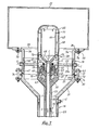
- FIG. 1 An outline structure of a sample application of the invention to a klystron is described using Figure 1.
- the components of the klystron tube an intermediate resonant cavity 11, drift tube 12, output cavity 13 and collector 14 are arranged vertically along the axis of the tube.
- a coaxial line section 17, comprising an internal conductor 15 and an external conductor 16 is coupled to part of the cavity wall of output cavity 13, and coolant is circulated in internal conductor 15, as shown by the arrows (C).
- the internal and external conductors both increase in diameter partway along, becoming the internal conductor large diameter section 18, and the external conductor large diameter section 19 respectively.
- a dielectric air-tight ring 20 is fixed so that it is vacuum tight between the two conductors at the large diameter section. Both conductors are split into components, as described below, at division 21 which is inside the position of the air-tight ring 20, and when the tube is complete, and the components are solidly coupled both electrically and hermetically.
- the end section 25 of internal conductor large diameter section 18 protrudes to a fixed. length only into the waveguide from coupling hole 24 in the waveguide.
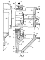
- Fig.2 is a broken down half-section of the essential parts to explain the order of assembly
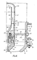
- Fig.3 is a vertical section showing the completed structure.
- the external conductor 16 of coaxial line section 17 connected to the klystron output cavity has, after an elongated section with a fixed diameter, an external conductor funnel-shaped section 31 which changes into large diameter section 19.
- No.1 flange 32 and external conductor No.1 thin weld ring 33 are soldered on at the open end of the large diameter section, and an indentation for the external conductor contact is made on the end surface.
- Internal conductor 15 is set coaxially on the inside of this external conductor.
- This comprises the internal conductor outer tube 35 and internal conductor inner tube 36, with a coolant path 37 inside.
- An internal conductor funnel section 38 is joined to internal conductor tube 35, and a connecting ring 39 for the internal conductor is joined to its end.
- an internal conductor No.1 thin weld ring 41 with a U-shaped half-section 40, and a contact edge 42 is formed at its end.
- An outer tube cylinder 44 with many diagonal slits 43 in part of it is joined to funnel-shaped section 38 of the internal conductor, and several screw holes 45 are formed at the end.
- An inner tube screw cylinder 46 having a female screw thread is joined to the end of the internal conductor inner tube.
- the section with dielectric air-tight ring 20 is assembled as a separate structure from this as follows.
- a thin outside wall 48 of an external conductor connecting ring 47 is given an air-tight join to the outside edge of ceramic dielectric air-tight ring 20, and several Molybdenum (Mo) external reinforcement rings 49 are wrapped around the outside.
- the bottom edge of external conductor connecting ring 47 has a tapered edge 50 for external conductor contact, and an external conductor No.2 thin weld ring 51 and an No.2 flange 52 are brazed onto the outside.
- External conductor connecting ring 47 is joined to external conductor end cylinder 54 so as to form a ring-shaped coolant chamber 53 around thin outer wall 48, and the coolant pipe 55 is fitted to part of this.
- No.3 flange 56 is fitted to the end section of cylinder 54 above.
- a thin inner wall 58 joined to an inner conductor connecting ring 57 is given an air-tight join to the inner edge of the dielectric air-tight ring 20, and a molybdenum reinforcing ring 59 is positioned inside it.
- a cylindrical internal conductor No.2 thin weld ring 60 is brazed to the inside of the internal conductor connecting ring 57, and an internal conductor No.1 weld ring 61 is joined to the top end of thin inner wall 58.
- a TiN multipactor suppression coating layer 20a is applied to the vacuum side of dielectric air-tight ring 20. (K.M.Welch "New materials and technology for suppression of RF multipactor" 1974 IEEE International Electron Devices Meeting Technical Digest.) As described above, these structures are assembled as a single unit.
- the section with the dielectric air-tight ring joined in an air-tight way between the internal and external conductors can be assembled separately from the tube as a single structure.
- high reliability can be readily achieved for the air-tight joints at the inner and outer edges of the dielectric air-tight ring, and for the application of the mutipactor suppression coating layer.
- high frequency current does not flow through the air-tight joints formed by the external conductor thin weld rings and the internal conductor thin weld rings, there is little possibility of these joints being damaged.
- the internal and external conductor walls are constructed so that high frequency current can actually flow through them, through the external conductor connecting ring and internal conductor connecting rings. Because of this, the structure can sufficiently withstand high power microwave transmission.
- a press ring 62 is prepared separately from the above structure.
- This press ring 62 has many diagonal slits 63, and several bolt holes 65 for the insertion of bolts 64.
- Internal conductor end section 25 having an inner tube cylinder 66 and an outer tube cylinder 67 is also prepared separately.
- An inner tube funnel-shaped section 68 is attached to the bottom end of inner tube cylinder 66, and an inner tube screw cylinder 69 which has a female screw thread is joined to it.
- Internal conductor No.2 weld ring 70 is joined to the bottom end of outer tube cylinder 67.
- Internal conductor end section 25 is joined to the top end of outer tube cylinder 67 at an outer tube connecting section 71 by brazing.
- the structure from the klystron output cavity to funnel-shaped section 31, 38 of internal and external conductors in coaxial section 17 is assembled as a single structure, and the structure containing dielectric air-tight ring section 20 is coupled to it. That is to say, at large diameter section 19 of the external conductor, external conductor No.1 thin weld ring 33 on external conductor funnel-shaped section 31 and external conductor No.2 thin weld ring 51 on external conductor connecting ring 47 are brought together, and their edges are sealed by argon-arc welding.
- internal conductor No.1 thin weld ring 41 on internal conductor funnel-shaped section 38 and internal conductor No.2 thin weld ring 60 on internal conductor connecting ring 57 are brought together and their edges are welded by argon-arc welding. These air-tight joints are denoted respectively by 72 and 73.
- external conductor No.1 flange 32 and No.2 flange 52 are clamped together by several clamping bolts 74, and on the internal conductor side, press ring 62 is inserted from above until it reaches internal conductor connecting ring 57, and is fastened on by screwing bolts 64 into bolt screw holes 45 in outer tube cylinder 44.
- coupling aperture 24 of waveguide 22 is brought together with No.3 flange 56 of external conductor cylinder end 54, and coupled with bolts 76.
- coolant is circulated, as shown by various arrows (C), through a coolant path 77 of the external conductor, coolant path 37 of the internal conductor, and through coolant chamber 53 around dielectric air-tight ring 20.
- the coolant flows mainly through slits 43 in outer cylinder 44, sufficiently cools internal conductor thin weld rings 41, 60, positioned inside the coolant circulation path, passes through slits 63 in press ring 62, cools thin inside wall 58, outer tube cylinder 67 and the internal conductor end section, flows into inner tube cylinder 66, and is discharged to the outside through internal conductor inner tube 36.
- cup-shaped internal conductor end section 25 is coupled so that it can be removed and refitted by screwing it on at a position outside that of dielectric air-tight ring 20 with a screw section 81.
- An O-ring 82 is added on the inside to form a watertight seal.
- the embodiment shown in Fig.5 has outer tube cylinder 67 of the internal conductor end section made even longer, with pipes 83, 85 for the supply and discharge of coolant at its end.
- Outer tube cylinder 67 is coupled by welding at a position outside that of dielectric air-tight ring 20.
- This output section has a coaxial waveguide section 85 protruding from the opposite face of the output waveguide so that it coaxially surrounds the internal conductor end section, and so that its bottom is electrically coupled with the outer tube cylinder 67, 86 are the fastening bolts.
- internal conductor end section 25 with the required length to correspond to the characteristics of the output waveguide can be fitted.
- the invention having the above configuration is formed with the coaxial line section having a division into 2 coaxial line divided blocks in the line axis direction at a position inside, i.e.., on the output cavity side of, that where the dielectric air-tight ring is attached in an air-tight manner between the outer wall of the internal conductor and the inner wall of the external conductor. Since the thin weld rings joined to each of the conductor walls at the division point are welded so as to be air-tight, the block on the side of the dielectric air-tight ring forming an air-tight joint between the internal and external conductors can be assembled as a single unit independent of the tube. Because of this, an extremely reliable joint structure can be easily achieved for each of the air-tight joint sections.
- the dielectric air-tight ring is attached to the large diameter section of the coaxial line, high frequency electric field density in the dielectric air-tight ring is reduced, preventing damage due to electric discharge and thermal stress, and moreover, prevention of part of the electron beam reaching the dielectric air-tight ring is ensured. Accordingly, because the coaxial line section can be made to be straight, each component shape is simple and easy to assemble. Moreover, an internal conductor end section with length, thickness and shape corresponding to the requirements of the output waveguide can be connected after evacuation of the tube, and fine adjustment of the coupling characteristics can also be easily carried out. This is a remarkable advantage for the output section of this type.
Landscapes
- Microwave Tubes (AREA)
- Waveguide Connection Structure (AREA)
Applications Claiming Priority (4)
| Application Number | Priority Date | Filing Date | Title |
|---|---|---|---|
| JP20355484A JPS6182639A (ja) | 1984-09-28 | 1984-09-28 | マイクロ波電子管の出力部 |
| JP203554/84 | 1984-09-28 | ||
| JP1984146776U JPH0438448Y2 (fr) | 1984-09-28 | 1984-09-28 | |
| JP146776/84U | 1984-09-28 |
Publications (3)
| Publication Number | Publication Date |
|---|---|
| EP0183355A2 true EP0183355A2 (fr) | 1986-06-04 |
| EP0183355A3 EP0183355A3 (en) | 1988-04-06 |
| EP0183355B1 EP0183355B1 (fr) | 1991-01-02 |
Family
ID=26477509
Family Applications (1)
| Application Number | Title | Priority Date | Filing Date |
|---|---|---|---|
| EP85306930A Expired EP0183355B1 (fr) | 1984-09-28 | 1985-09-27 | Couplage de sortie d'un tube à micro-ondes |
Country Status (3)
| Country | Link |
|---|---|
| US (1) | US4683401A (fr) |
| EP (1) | EP0183355B1 (fr) |
| DE (1) | DE3581062D1 (fr) |
Cited By (3)
| Publication number | Priority date | Publication date | Assignee | Title |
|---|---|---|---|---|
| EP0312446A1 (fr) * | 1987-10-16 | 1989-04-19 | Thomson-Csf | Dispositif de refroidissement pour circuits hyperfréquence |
| EP0241943A3 (en) * | 1986-04-18 | 1989-05-03 | Kabushiki Kaisha Toshiba | Microwave apparatus having coaxial waveguide partitioned by vacuum-tight dielectric plate |
| EP1675150A3 (fr) * | 2004-12-24 | 2007-07-18 | E2V Technologies (UK) Limited | Arrangement de sortie pour un tube à faisceau d'électrons |
Families Citing this family (2)
| Publication number | Priority date | Publication date | Assignee | Title |
|---|---|---|---|---|
| US5130601A (en) * | 1990-03-14 | 1992-07-14 | Litton Systems, Inc. | Quick warm-up cathode heater for high average power magnetrons |
| RU2674750C1 (ru) * | 2018-01-15 | 2018-12-13 | Российская Федерация, от имени которой выступает Государственная корпорация по атомной энергии "Росатом" (Госкорпорация "Росатом") | Устройство согласования замедляющей системы |
Family Cites Families (8)
| Publication number | Priority date | Publication date | Assignee | Title |
|---|---|---|---|---|
| US2608673A (en) * | 1949-10-25 | 1952-08-26 | Raytheon Mfg Co | Electron discharge device |
| US3254263A (en) * | 1960-05-04 | 1966-05-31 | Varian Associates | High frequency tube apparatus with improved output coaxial connector |
| US3227915A (en) * | 1960-10-17 | 1966-01-04 | Eitel Mccullough Inc | Fluid cooling of hollow tuner and radio frequency probe in klystron |
| US3252034A (en) * | 1962-04-16 | 1966-05-17 | Eitel Mccullough Inc | R-f window for high power electron tubes |
| US3439296A (en) * | 1967-04-20 | 1969-04-15 | Varian Associates | Microwave window employing a half-wave window structure with internal inductive matching structure |
| US3701061A (en) * | 1970-10-20 | 1972-10-24 | Atomic Energy Commission | Radiofrequency window assembly having shielded solder joints and reweldable replacement flanges |
| FR2137311B1 (fr) * | 1971-05-18 | 1973-05-11 | Thomson Csf | |
| US3891884A (en) * | 1972-06-26 | 1975-06-24 | Raytheon Co | Electron discharge device having electron multipactor suppression coating on window body |
-
1985
- 1985-09-26 US US06/780,308 patent/US4683401A/en not_active Expired - Fee Related
- 1985-09-27 DE DE8585306930T patent/DE3581062D1/de not_active Expired - Lifetime
- 1985-09-27 EP EP85306930A patent/EP0183355B1/fr not_active Expired
Cited By (5)
| Publication number | Priority date | Publication date | Assignee | Title |
|---|---|---|---|---|
| EP0241943A3 (en) * | 1986-04-18 | 1989-05-03 | Kabushiki Kaisha Toshiba | Microwave apparatus having coaxial waveguide partitioned by vacuum-tight dielectric plate |
| EP0312446A1 (fr) * | 1987-10-16 | 1989-04-19 | Thomson-Csf | Dispositif de refroidissement pour circuits hyperfréquence |
| FR2622048A1 (fr) * | 1987-10-16 | 1989-04-21 | Thomson Csf | Dispositif de refroidissement pour circuits hyperfrequence |
| US5006825A (en) * | 1987-10-16 | 1991-04-09 | Thomson-Cf | Coaxial line coupler with fluid cooled inner conductor |
| EP1675150A3 (fr) * | 2004-12-24 | 2007-07-18 | E2V Technologies (UK) Limited | Arrangement de sortie pour un tube à faisceau d'électrons |
Also Published As
| Publication number | Publication date |
|---|---|
| EP0183355B1 (fr) | 1991-01-02 |
| EP0183355A3 (en) | 1988-04-06 |
| US4683401A (en) | 1987-07-28 |
| DE3581062D1 (de) | 1991-02-07 |
Similar Documents
| Publication | Publication Date | Title |
|---|---|---|
| EP0241943B1 (fr) | Dispositif aux micro-ondes comportant un guide coaxial pourvu d'une fenêtre diélectrique étanche au vide | |
| US4705989A (en) | Magnetron with a ceramic stem having a cathode support structure | |
| EP0183355B1 (fr) | Couplage de sortie d'un tube à micro-ondes | |
| US3876901A (en) | Microwave beam tube having an improved fluid cooled main body | |
| US3325671A (en) | Klystron device having fluid cooled tunable cavities and output window mode suppression means | |
| US2768327A (en) | Wave guide output circuit for a magnetron | |
| US3707647A (en) | High frequency vacuum tube energy coupler | |
| US4970432A (en) | Travelling wave tube with coupling device between its delay line and external microwave circuits | |
| JPH0427082Y2 (fr) | ||
| JPH0438448Y2 (fr) | ||
| US3348088A (en) | Electron tube apparatus | |
| JPH0756782B2 (ja) | マイクロ波電子管の出力部構体 | |
| US3334262A (en) | High frequency velocity modulation electron discharge devices having replaceable beam forming and projecting assemblies | |
| JPS6323871Y2 (fr) | ||
| JP3039956B2 (ja) | マグネトロン陰極構体 | |
| JPH0453063B2 (fr) | ||
| JPS62246228A (ja) | 同軸導波管構体 | |
| JP2597386B2 (ja) | ジャイロトロン | |
| JPH0250501A (ja) | 同軸導波管構体 | |
| JP3170106B2 (ja) | 高周波結合器 | |
| KR0123822Y1 (ko) | 마그네트론 요우크의 결합장치 | |
| US2890371A (en) | Travelling wave tubes | |
| JP2602297B2 (ja) | ジャイロトロン | |
| JPH0127543B2 (fr) | ||
| JPH0523397U (ja) | 進行波管用rf出力窓 |
Legal Events
| Date | Code | Title | Description |
|---|---|---|---|
| PUAI | Public reference made under article 153(3) epc to a published international application that has entered the european phase |
Free format text: ORIGINAL CODE: 0009012 |
|
| 17P | Request for examination filed |
Effective date: 19851018 |
|
| AK | Designated contracting states |
Kind code of ref document: A2 Designated state(s): DE FR GB |
|
| PUAL | Search report despatched |
Free format text: ORIGINAL CODE: 0009013 |
|
| AK | Designated contracting states |
Kind code of ref document: A3 Designated state(s): DE FR GB |
|
| 17Q | First examination report despatched |
Effective date: 19891106 |
|
| GRAA | (expected) grant |
Free format text: ORIGINAL CODE: 0009210 |
|
| AK | Designated contracting states |
Kind code of ref document: B1 Designated state(s): DE FR GB |
|
| ET | Fr: translation filed | ||
| REF | Corresponds to: |
Ref document number: 3581062 Country of ref document: DE Date of ref document: 19910207 |
|
| PGFP | Annual fee paid to national office [announced via postgrant information from national office to epo] |
Ref country code: GB Payment date: 19910806 Year of fee payment: 7 |
|
| PLBE | No opposition filed within time limit |
Free format text: ORIGINAL CODE: 0009261 |
|
| STAA | Information on the status of an ep patent application or granted ep patent |
Free format text: STATUS: NO OPPOSITION FILED WITHIN TIME LIMIT |
|
| 26N | No opposition filed | ||
| PG25 | Lapsed in a contracting state [announced via postgrant information from national office to epo] |
Ref country code: GB Effective date: 19920927 |
|
| GBPC | Gb: european patent ceased through non-payment of renewal fee |
Effective date: 19920927 |
|
| PGFP | Annual fee paid to national office [announced via postgrant information from national office to epo] |
Ref country code: FR Payment date: 19940909 Year of fee payment: 10 |
|
| PGFP | Annual fee paid to national office [announced via postgrant information from national office to epo] |
Ref country code: DE Payment date: 19940921 Year of fee payment: 10 |
|
| PG25 | Lapsed in a contracting state [announced via postgrant information from national office to epo] |
Ref country code: FR Effective date: 19960531 |
|
| PG25 | Lapsed in a contracting state [announced via postgrant information from national office to epo] |
Ref country code: DE Effective date: 19960601 |
|
| REG | Reference to a national code |
Ref country code: FR Ref legal event code: ST |