EP0183592A1 - Asynchrone Paketvermittlung - Google Patents
Asynchrone Paketvermittlung Download PDFInfo
- Publication number
- EP0183592A1 EP0183592A1 EP85402159A EP85402159A EP0183592A1 EP 0183592 A1 EP0183592 A1 EP 0183592A1 EP 85402159 A EP85402159 A EP 85402159A EP 85402159 A EP85402159 A EP 85402159A EP 0183592 A1 EP0183592 A1 EP 0183592A1
- Authority
- EP
- European Patent Office
- Prior art keywords
- packet
- circuit
- outgoing
- memory
- path
- Prior art date
- Legal status (The legal status is an assumption and is not a legal conclusion. Google has not performed a legal analysis and makes no representation as to the accuracy of the status listed.)
- Withdrawn
Links
- 230000015654 memory Effects 0.000 claims abstract description 140
- 238000012546 transfer Methods 0.000 claims abstract description 112
- 239000011159 matrix material Substances 0.000 claims description 32
- 230000005540 biological transmission Effects 0.000 claims description 20
- 239000003550 marker Substances 0.000 claims description 20
- 238000012423 maintenance Methods 0.000 claims description 8
- 230000006870 function Effects 0.000 claims description 6
- 101001091388 Homo sapiens Kallikrein-7 Proteins 0.000 claims description 4
- 102100034867 Kallikrein-7 Human genes 0.000 claims description 4
- 230000005055 memory storage Effects 0.000 claims 1
- 238000012986 modification Methods 0.000 claims 1
- 230000004048 modification Effects 0.000 claims 1
- 238000007493 shaping process Methods 0.000 claims 1
- 230000002123 temporal effect Effects 0.000 claims 1
- 230000000712 assembly Effects 0.000 abstract description 4
- 238000000429 assembly Methods 0.000 abstract description 4
- 238000004891 communication Methods 0.000 abstract description 3
- 230000000007 visual effect Effects 0.000 abstract 1
- 238000010586 diagram Methods 0.000 description 11
- 230000003287 optical effect Effects 0.000 description 10
- 229920006395 saturated elastomer Polymers 0.000 description 6
- 238000013475 authorization Methods 0.000 description 5
- 238000001514 detection method Methods 0.000 description 5
- 230000008901 benefit Effects 0.000 description 3
- 238000000034 method Methods 0.000 description 3
- 238000012545 processing Methods 0.000 description 2
- 101000861263 Homo sapiens Steroid 21-hydroxylase Proteins 0.000 description 1
- 102100027545 Steroid 21-hydroxylase Human genes 0.000 description 1
- 230000006978 adaptation Effects 0.000 description 1
- 230000003466 anti-cipated effect Effects 0.000 description 1
- 210000001367 artery Anatomy 0.000 description 1
- 230000001143 conditioned effect Effects 0.000 description 1
- 238000012217 deletion Methods 0.000 description 1
- 230000037430 deletion Effects 0.000 description 1
- 238000005516 engineering process Methods 0.000 description 1
- 230000007246 mechanism Effects 0.000 description 1
- 238000002360 preparation method Methods 0.000 description 1
- 230000035484 reaction time Effects 0.000 description 1
- 230000009467 reduction Effects 0.000 description 1
- 230000009466 transformation Effects 0.000 description 1
Images





Classifications
-
- H—ELECTRICITY
- H04—ELECTRIC COMMUNICATION TECHNIQUE
- H04L—TRANSMISSION OF DIGITAL INFORMATION, e.g. TELEGRAPHIC COMMUNICATION
- H04L49/00—Packet switching elements
- H04L49/10—Packet switching elements characterised by the switching fabric construction
- H04L49/104—Asynchronous transfer mode [ATM] switching fabrics
- H04L49/105—ATM switching elements
- H04L49/108—ATM switching elements using shared central buffer
-
- H—ELECTRICITY
- H04—ELECTRIC COMMUNICATION TECHNIQUE
- H04L—TRANSMISSION OF DIGITAL INFORMATION, e.g. TELEGRAPHIC COMMUNICATION
- H04L49/00—Packet switching elements
- H04L49/10—Packet switching elements characterised by the switching fabric construction
- H04L49/104—Asynchronous transfer mode [ATM] switching fabrics
- H04L49/105—ATM switching elements
- H04L49/106—ATM switching elements using space switching, e.g. crossbar or matrix
-
- H—ELECTRICITY
- H04—ELECTRIC COMMUNICATION TECHNIQUE
- H04L—TRANSMISSION OF DIGITAL INFORMATION, e.g. TELEGRAPHIC COMMUNICATION
- H04L49/00—Packet switching elements
- H04L49/15—Interconnection of switching modules
- H04L49/1515—Non-blocking multistage, e.g. Clos
-
- H—ELECTRICITY
- H04—ELECTRIC COMMUNICATION TECHNIQUE
- H04L—TRANSMISSION OF DIGITAL INFORMATION, e.g. TELEGRAPHIC COMMUNICATION
- H04L49/00—Packet switching elements
- H04L49/20—Support for services
- H04L49/205—Quality of Service based
- H04L49/206—Real Time traffic
Definitions
- the present invention relates to an asynchronous packet switch.
- the switch described intended for use in a packet switched network, manages packets comprising a header indicating the final destination of the packet.
- Such a type of switch is described, for example, in French patent n ° 80 06210 (2 478 911) filed on March 20, 1980 by the applicant.
- the switch described in this patent includes means for reading the header of the packet and means for determining, from routing tables, the output of the switch to which the packet must be sent. It includes a first stage of spatial preselection allowing incoming interface sections to access a second time stage composed of groups of memory cells of the size of a packet. The outputs of the memory cells are connected to the outgoing interface sections by means of a third spatial mixing stage and a fourth final selection spatial stage.
- the advantages of such a switch are great flexibility of adaptation, high resistance to partial failures of the elements of the switch and, at the network level, a low vulnerability to switch failure and the possibility of dynamic equalization. of the load of the transmission arteries.
- the present invention relates to an asynchronous packet switch making it possible to remedy these drawbacks and to push the usable technologies to the limits of their possibilities.
- the present invention describes a switch for a multiservice network including video communication and which, thanks to identical standardized memories, can transmit large packets for high speed links.
- This switch can, in addition, switch a large number of packets in parallel thanks to a packet transfer network with high marking power.
- the switch provides a step of receiving the packet in the memory and a step of transmitting the packet on the chosen output line, the two steps are doing asynchronously according to the state of the different stages of the switch.
- the structure of the switch allows the storage of the incoming packet in one of two subgroups of t memories, t being a natural integer, and this, from the start of reception of the incoming packet .
- the packet header is analyzed during storage and the characteristics of said packet are sent to the chosen output circuit.
- the output circuit requests a path connection in the packet transfer network before the end of transmission of the previous packet and sends the packet request as soon as the end of transmission of the previous packet.
- Direct control signals such as maintaining matrix cross points, start, next end, end of packet and request to send packet, are transmitted by planes parallel to those of the packet transfer network.
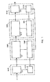
- FIG. 1 the various main parts of the packet switch according to the invention are represented, composed of groups of incoming circuits GCE, groups of packet memories GMP, three spatial switching stages SSS and groups of outgoing circuits GCS.
- Incoming packets are transmitted by an incoming circuit CE, controlled by an incoming circuit control circuit CCE, to a space-time stage ST, itself controlled by a packet memory control circuit CMP which exchanges information with the incoming circuit control circuits CCE and the outgoing circuit control circuits CCS.
- These packets are transmitted to the outgoing circuit CS through a packet transfer network RTP composed of several transfer matrix plans, the latter being controlled by a marker MQ exchanging information with the outgoing circuit control circuit CCS.
- An incoming circuit CE which receives an incoming packet, directs the needle to a group of packet memories GMP, thanks to the incoming circuit control circuit CCE.
- the incoming packet is sent to one of two subgroups of packet memories, depending on the sequence of incoming packets, either alternately or depending on the availability of these subgroups of packet memories.
- the group of packet memories GMP comprises a spatial stage which sends the packet entering a packet memory of the time stage thanks to the circuit of control of packet memories CMP.
- This packet memory control circuit CMP receives the packet memory requests from the group of incoming circuits GCE and sends it the availability information of the packet memory subgroups.
- the outgoing circuit CS which the packet must borrow, is determined by the packet memory control circuit CMP, according to its state of charge sent by the circuit of CCS outgoing circuit control, and a routing table. As soon as the incoming packet is stored, the characteristics of the packet are sent by the same packet memory control circuit CMP to the chosen outgoing circuit control circuit CCS. As soon as the CMP packet memory control circuit sends it a signal for the next end of the previous outgoing packet, the CCS outgoing circuit control circuit requests the marker MQ to connect it a path in the RTP packet network from the memory package containing the package.
- the marker MQ determines the path, before arrival at the outgoing circuit control circuit CCS, of the previous outgoing packet end signal. Upon receipt of this signal, the outgoing circuit control circuit CCS requests the packet memory control circuit CMP sending the packet to the outgoing circuit CS. This makes it possible to significantly reduce the dead time between two packets sent on the same outgoing line LE.
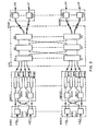
- FIG. 2 shows the more detailed structure of the packet transmission circuits in which there are, for example, two hundred and fifty-six incoming LE lines distributed in groups of eight out of thirty-two groups of incoming circuits GCEO to GCE31.
- each incoming line, LEO to LE7 passes through one of the incoming circuits CEO to CE7 which directs the incoming packets to one of two transfer matrices SO / 0 and SO / 1, the eight inputs are each connected to one of the two outputs of each incoming circuit CEO to CE7, and whose outputs are thirty-two in number.
- transfer matrices represent a first spatial stage and have their outputs each connected to a packet memory, thus forming two subgroups of thirty-two packet memories MPO to MP31 and MP32 to MP63.
- the sixty-four memories, associated with each group of incoming circuits and forming the time stage, constitute the packet memory groups GMPO to GMP31, the number of which is the same as that of the groups of incoming circuits GCE.
- Each of the thirty-two groups of GMP packet memories is connected to a transfer matrix with sixty-four inputs and thirty-two outputs, forming a first spatial stage SI of the RTP packet transfer network.
- a second spatial stage S2 of the RTP packet transfer network is formed of transfer matrices with thirty-two inputs, each connected to an output of each matrix of the first spatial stage SI, and with thirty-two outputs, each connected to an input of each transfer matrix of a third spatial stage S3.
- This third space stage S3, formed by thirty-two transfer matrices with sixteen outputs, makes it possible to connect thirty-two groups of outgoing circuits GCSO to GCS31 of eight outgoing circuits CSO to CS7 with two inputs, each of these outgoing circuits CS serving a outgoing line, LSO to LS7.
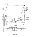
- the thirty-two groups of incoming circuits GCEO to GCE31, represented in FIG. 3, are each composed of eight incoming circuits CEO to CE7 each controlled by an incoming circuit control circuit, CCEO to CCE7.
- Each incoming circuit CE receives an incoming line LE by a line reception circuit CRL, then transmits the packets to a delay line LAR placed at the input of an access switch ASO directing the packets to two outputs, pair and odd, possible, 100 to 107 and, I10 to 117.
- These three circuits are connected to an SCCE incoming circuit supervision and control circuit itself connected to the CCE incoming circuit control circuit.
- the eight incoming circuit control circuits CCEO to CCE7 are connected on the one hand to the inputs of a multiplexer whose output, GCESO to GCES31, of each group of incoming circuits GCEO to GCE31 is connected respectively to one of the packet memory groups GMPO to GMP31, and on the other hand to the outputs of a demultiplexer whose input, GCEEO to GCEE31, of each group of incoming circuits GCEO to GCE31, comes respectively from one of the groups of memory memories GMPO to GMP31.
- the line reception circuit CRL performs the interface with the incoming line LE, proceeds to decode the signal online and transfers, by validating them, the useful bits received to the digital delay line LAR.
- This digital delay line LAR introduces a delay and acts as a buffer register.
- the incoming circuit supervision and control circuit SCCE sends packet reception start and end signals to the incoming circuit control circuit CCE and controls the switch ASO.
- the incoming circuit control circuit CCE preselects the position of the access switch ASO as a function of the previous position, and, when the incoming packet flow is not too large, of the occupation of the packet memory subgroups MP corresponding.
- the demultiplexer requests from the group of packet memories GMP, via the output GCES of the multiplexer, a packet memory MP from the start of reception of a packet in the line reception circuit CRL; the delay time of the LAR delay line gives the access switch ASO the reaction time necessary for its switchover.
- the input GCEE of the demultiplexer provides the control circuit of the incoming circuit CCE with the occupation status of the subgroups of packet memories MP. The procedure for receiving the package is described below.
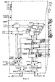
- FIG. 4 are represented the thirty-two groups of packet memories GMPO to GMP31 which each receive on two transfer matrices SO / 0 and SO / 1, the eight even outputs 100 to 107 and the eight odd outputs 110 to 117 of the group of associated GCE incoming circuits.
- the transfer matrices S0 / 0 and SO / 1 with eight inputs have thirty-two outputs each connected to a packet memory MP and are connected to two matrix markers MQSO and MQS1.
- the two subgroups of thirty-two packet memories MPO to MP31 and MP32 to MP63 have their packet memories each connected to a supervision circuit and packet control, SCMPO to SCMP31 and SCMP32 to SCMP63, and to the MQSO and MQSI matrix markers respectively.
- An incoming access control circuit CAE receives from the multiplexer of the group of incoming circuits GCE corresponding a first link GCES and sends to the demultiplexer a second link GCEE; in addition, it is connected to the two matrix markers MQSO and MQSI and to a load indicator calculation circuit of the packet memory group CICGMP.
- a routing translator circuit TACH is connected to the sixty-four supervision and control circuits of packet memory SCMPO to SCMP63 and to a circuit for managing new packets received GNPR.
- An ARGCS outgoing circuit group receive access circuit sends a saturated queue indicator signal IFAS and an ARP packet acknowledgment signal to the new received packet management circuit GNPR and furthermore it sends a binary volume signal of packets awaiting output VBPAS to the routing translator circuit TACH; these last three signals come from the outgoing circuit groups GCS via an input bus BE.
- a transmission access circuit to the outgoing circuit groups AEGCS receives a signal indicating load of the packet memory group ICGMP from the load indicator calculation circuit of the packet memory group CICGMP and a signal of characteristics of new packets received CNPR of the management circuit for new packets received GNPR and sends them to the outgoing circuit groups GCS on an output bus BS.
- the packet memory supervision and control circuits SCMPO to SCMP63 are connected to the outgoing circuit groups GCS by holding wires FME, forward control wires FCAE and return control wires FCRE transmitting direct control signals by the intermediary of the RTP packet transfer network, which comprises three plans of three stages S1, S2, S3 of transfer matrices, those of the first stage each receiving the sixty-four wires for maintaining or controlling a group of GMP packet memories .
- the packet memories proper MPO to MP31 each access the packet transfer network by p links, p being the number of information transfer plans of the RTP packet transfer network as will be seen below.
- the incoming access circuit CAE receives the packet memory request from the GCES output of the multiplexer of the group of corresponding incoming circuits and communicates it to the MQSO and MQSI matrix markers from which it receives. the state load of the packet memory subgroups which it communicates to the GCEE input of the demultiplexer of the group of incoming circuits GCE and to the load indicator calculation circuit of the packet memory group CICGMP.
- the matrix markers MQSO and MQSI direct the packets to the available packet memories MP, receive the information of availability of packet memories MP, send to the incoming circuit CAE the state of occupation of the MP packet memory subgroups and receive packet memory requests therefrom.
- the packet memory supervision and control circuits SCM P O to SCMP63 send to the MQSO or MQSI matrix marker corresponding to their subgroup, the state of availability of the packet memories and notify it of the end of reception of the packets.
- the packet memory supervision and control circuits SCMPO to SCMP63 communicate, after decoding, the headers of the packets to the routing translator circuit TACH, modify them on possible order of the routing translator circuit TACH, manage the signal exchanges direct control with outgoing circuits CS through the RTP packet transfer network and are notified by the matrix marker corresponding to their subgroup of the arrival of a packet.
- the routing translator circuit TACH translates the received header, sends transformation indications to the SCMP packet memory supervision and control circuit concerned, chooses the outgoing line LS on the basis of the load indications of the outgoing lines LS given by the binary volume of packets awaiting output VBPAS and transfers the characteristics of the received packet to the management circuit of new packets received GNPR.
- the circuit for managing new packets received GNPR manages the sending of the characteristic signals of new packets received GNPR to the transmission access circuit to the outgoing circuit groups AEGCS and receives in return the corresponding ARP packet acknowledgments, the sending being conditioned by the state of the saturated queue indicator IFAS broadcast by each group of outgoing circuits GCS to all the groups of packet memories GMPO to GMP31 and by the end of packet reception of the packets concerned.
- the circuit for calculating the load indicators of the packet memory group CICGMP calculates the load indicators of the packet memory group ICGMP highlighting an overload threshold of the packet memories MP and an access overload threshold of a group of packet memories GMP on the first stage S1 of the RTP packet transfer network.
- ARGCS and AEGCS outgoing circuit groups receive the IFAS overload queue indicators, the ARP packet acknowledgments and the binary volume of packets awaiting VBPAS output, and issue the ICGMP packet memory group charge indicators and the characteristics of new packets received CNPR, respectively on the input bus BE and on the output bus BS.
- FIG. 5 are represented the thirty-two groups of outgoing circuits GCSO to GCS31 each composed of eight outgoing circuits CSO to CS7 and their outgoing circuit control circuits CCSO to CCS7.
- the outgoing circuits CSG to CS7 receive the packets on an access switch AS3 with two entries EO and El, each entry comprising p links, p being the number of information transfer plans of the RTP packet transfer network, as is will see below.
- Each access switch AS3 also includes an output connected to an output buffer register RTS connected to a line transmission circuit CEL which serves an outgoing line LS.
- An output bus BS brings the indicators of load indicator of the packet memory group ICGMP and of characteristics of new packets received CNPR towards demultiplexers for reception of the groups of packet memory ARGMP whose eight outputs are connected to the control circuits of outgoing circuit CCSO to CCS7, themselves connected to transmission access multiplexers to the eight-input AEGMP packet memory groups and the output of which, on the input bus BE, the acknowledgment signals of ARP packet, binary volume of packets awaiting VBPAS output, and IFAS saturated queue indicator.
- the eight outgoing circuit control circuits CCSO to CCS7 receive a packet request signal following DPS from their outgoing circuit CS and send it a packet initialization signal according to IPS.
- a third multiplexer with eight inputs, each connected to an outgoing circuit control circuit CCSO to CCS7, has its output connected to an access circuit to the AMQ marker, the output of which gives the addresses of ends to be connected AEACO to AEAC31.
- the access switch AS3 on the third stage S3 of the RTP packet transfer network makes it possible to switch from one access to the other to receive the next packet to be transmitted at the end of the previous packet.
- the buffer register of RTS output allows compliance with the transmission protocol used on the outgoing line.
- the line transmission circuit CEL performs the functions of coding the online signal.
- the supervision and control circuit of the outgoing circuit SCCS exchanges and manages direct control signals, by doubled wires for maintaining FMS, doubled wires for forward control FCAS and doubled wires for return control FCRS, with packet memory groups GMP through the RTP packet transfer network, ensures the control of the access switch AS3, causes the transmission of jamming patterns on the outgoing line, signals to the outgoing circuit control circuit CCS the next end of the current packet transmission by a packet request following DPS and is warned by the outgoing circuit control circuit CCS of the imminence of the latter by the packet initialization signal following IPS.
- FIG. 6 shows the CCS outgoing circuit control circuit composed of a next packet pick-up circuit PRPPP receiving the packet request signal following DPS, transmitting the packet initialization signal IPS and connected to a next packet selection circuit SPPP, itself connected to a dynamic state circuit of the outgoing line EDLS which receives information from the output buffer register RTS, to a packet address queue circuit in waiting FAAPA, and receiving the load indicator signals from the packet memory group ICGMP.
- a circuit for reception of new packets received RNPR receives the signal for characteristics of new packets received CNPR and delivers the signals of acknowledgment of packet ARP and indicator of saturated queue IFAS, by being connected to the queue circuit waiting for addresses of packets waiting FAAPA which receives an update signal MAJ from the selection circuit of the next packet prepared SPPP.
- a next prepared packet PPP register is connected to the next prepared packet selection circuit SPPP and to a transfer authorization circuit CAT which likewise receives an output from the next prepared packet pickup circuit PRPPP and which delivers the signal d 'end addresses to connect AEAC.
- a circuit for calculating the binary volume of packets awaiting output CALVBPAS connected to the queue circuit for addressing addresses of packets awaiting FAAPA, delivers the signal for the binary volume of packets awaiting output VBPAS.
- the circuit for receiving new packets received RNPR transmits the characteristics of new packets received CNPR in the packet address queue circuit in FAAPA wait and sends ARP packet acknowledgment and IFAS queue queue indicator signals to GMP packet banks based on information sent by the packet address queue circuit waiting FAAPA.
- the next prepared packet selection circuit SPPP chooses the addresses of the next packets to be transmitted according to the load indicator signal of groups of ICGMP packet memories and the priority of the packets in the waiting queue circuit of FAAPA packet addresses , and makes this choice periodically until the dynamic outgoing line state circuit EDLS, which receives its information from the output buffer register RTS and manages the sending of packets according to the transmission protocol on the outgoing line LS, authorizes sending the package.
- the dynamic outgoing line state circuit EDLS which receives its information from the output buffer register RTS and manages the sending of packets according to the transmission protocol on the outgoing line LS, authorizes sending the package.
- the content of the register of next packet prepared PPP, chosen by the selection circuit of next packet prepared SPPP, is transferred, by the transfer authorization circuit CAT to the access circuit to the marker AMQ, on command of the circuit for taking the next prepared packet PRPPP, itself informed of the transfer instant by the next prepared packet selection circuit SPPP and by the next packet request signal DPS. Therefore, the signal of end addresses to be connected AEAC is transmitted after the arrival of the packet request signal following DPS as soon as the next packet selection circuit prepared SPPP, on information from the outgoing line dynamic state circuit.
- EDLS authorizes it and the fact that a new packet will be transferred is signaled by the next packet initialization signal IPS, while the update signal MAJ commands the deletion of the references of the transmitted packet.
- the binary volume of packets waiting for output VBPAS gives the state of charge of the outgoing line LS, according to the length of the packets waiting, and the saturated queue indicator IFAS gives the state of occupation of the FAAPA packet address queue queuing queue.
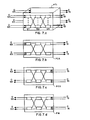
- FIGs 8.a to 8.d is shown the sequence of reception of an incoming packet.
- the ASO switch is assumed to have been preselected according to the availability of the packet memory subgroups and the transfer matrix chosen SO / 0 or SO / 1 (FIG. 4) selects an MPX packet memory by a first path, as shown in Figure 8.a.
- the other transfer matrix receives a packet memory request and takes advantage of the delay provided by. the delay line LAR to select a second path to reach an MPY packet memory of the other subgroup, as shown in Figure 8.b.
- the MQSO or MQS1 matrix marker concerned disconnects the - first path in the transfer matrix, as shown in FIG. 8.c.
- the CRL line reception circuit causes the ASO access switch to switch to the other output with a delay compatible with that of the LAR delay line with respect to the start of reception of the second packet Pj + 1 of the burst as shown figure 8.d. Thus the switching takes place between the first and the second pack.
- the access switch ASO preselects an even or odd output depending on the availability of the packet memory subgroups; otherwise it switches to the even and odd outputs alternately.
- the access switch ASO preselects an even or odd output depending on the availability of the packet memory subgroups; otherwise it switches to the even and odd outputs alternately.
- the access switch ASO preselects an even or odd output depending on the availability of the packet memory subgroups; otherwise it switches to the even and odd outputs alternately.
- the access switch ASO preselects an even or odd output depending on the availability of the packet memory subgroups; otherwise it switches to the even and odd outputs alternately.
- the access switch ASO preselects an even or odd output depending on the availability of the packet memory subgroups; otherwise it switches to the even and odd outputs alternately.
- the access switch ASO preselects an even or odd output depending on the availability of the packet memory subgroups; otherwise it switches to the even and odd outputs alternately.
- the access switch ASO preselects an even or odd output depending
- the packet is then identified and the end addresses to be connected to AEAC are sent to the MQ marker so that it searches for and connects a path.
- the outgoing circuit CS then receives the packet initialization signal following IPS.
- the switch AS3 of the outgoing circuit toggles, a packet send request signal is then sent to the group of packet memories concerned on the FCR wire and the wire. hold FM corresponding to the first output of the transfer matrix of the third stage S3 is released, thereby disconnecting the crossover points from the path of the previous packet.
- the time T separating the next end signal from the packet and the end signal from the packet is a system constant which results from a compromise between the probability of not being able to supply the outgoing line LS, while a packet is pending, and the additional fictitious traffic volume in the RTP packet transfer network resulting from the anticipated path take.
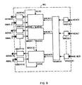
- FIG. 9 shows the marker MQ receiving the thirty-two end address signals to be connected AEACO to AEAC31 coming from the thirty-two circuits for accessing the markers AMQO to AMQ31 from the outgoing circuit groups, and likewise receiving thirty-two mesh address signals to be released AMALO to AMAL31 from the RTP packet transfer network.
- the MQ marker is composed of thirty-two access circuits for receiving the control circuit of the outgoing circuit ARCCSO to ARCCS31, receiving the address signals of ends to be connected AEACO to AEAC31 connected to a distributor circuit for access to the modules.
- RAMRCH path search of which the thirty-two outputs of new end addresses to connect NAEACO to NAEAC31 are connected to thirty-two path search modules MRCHO to MRCH31 connected in a ring.
- path search modules are each connected to a transmission access circuit to the packet transfer network, AERTPO to AERTP31, which transmits the path address signals to be connected ACHACO to ACHAC31 and to a reception access circuit at ARRTPO packet forwarding network to ARRTP31, which receives the mesh address signals to be released AMALO to AMAL31 from the transfer matrices of the second and third stages S2, S3 of the RTP packet transfer network.
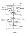
- path search modules MRCH (here MRCHi and MRCHi + 1) at the entrance of which is a register of end addresses to be connected RAEAC connected to a first transfer authorization circuit 1 controlled by a complemented path signal found CHT and likewise connected to a path search circuit CRCH which receives the signal of mesh addresses to be released AMAL and transmits the path address signal to be connected ACHAC.
- This path search circuit CRCH delivers the path signal found CHT which controls a second transfer authorization circuit 2 the input of which is connected to the output of a register of new end addresses to be connected RNAEAC receiving the output from the FAAEAC connect end queue which receives the new NAEAC connect end addresses.
- the outputs of the two transfer authorization circuits 1 and 2 are connected to a logic "OR" circuit 3, the output of which is connected to the input of the register of ends of addresses to be connected RAEAC of the following path search module .
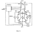
- FIG. 11 a path search circuit CRCHi composed of a first and a second availability circuit of meshes A and B, DISPMAi, DISPMBi, the thirty-two inputs of which are connected to a first and a second demultiplexer.
- DMXAi, DMXBi respectively and whose thirty-two outputs are connected to a first and a second multiplexer MXAi, MXBi respectively.
- the meshes A and B respectively bring together the first on the second stage and the second on the third stage of transfer matrices.
- the first multiplexers and demultiplexers are controlled by an input connected to the part of the signal of end addresses to be connected AEAC which identifies the group of GMP packet memories.
- the second multiplexers and demultiplexers are controlled by an input connected to the part which identifies the group of outgoing circuits GCS.
- the outputs of said multiplexers are connected to an "AND" logic circuit 4i, the output of which is connected to the input of a bistable circuit B which emits the path signal found CHTi at the input of the two demultiplexers and on a circuit of preparation of the path address to connect PRACHACi which also receives the end address to connect AEAC and gives the output the path address to connect ACHACi.
- a path search and connection request from a CCS outgoing circuit control circuit is put in the queue of FAAEAC endpoints to be connected (FIG. 10) of a given MRCH path search module.
- the thirty-two path search modules MRCH operate simultaneously and in synchronism to find a path in their respective transfer matrix of the second stage S2, thus carrying out thirty-two simultaneous path searches per time cycle.
- the path search circuit CRCH finds a path (path signal found CHT at logic level 1), it prepares the corresponding connection orders for the transfer matrices concerned from the first, second and third stages of the RTP packet transfer network. At the following time, it is therefore a new request for end addresses to connect NAEAC coming from the queue of end address to connect FAAEAC, via the register of new end addresses for connect RNAEAC, which is transferred to the register of endpoints to connect RAEAC of the next MRCH path search module.
- the path search circuit CRCH does not find a path (path signal found CHT at logic level 0), it is the content of the register of end addresses to be connected RAEAC of this module which is transferred -in the register of end addresses to connect RAEAC of the following MRCH path search module.
- each path search circuit CRCH associated with a particular matrix of the second stage S2, there exists only one mesh MA between the first and second stages S1, S2 to reach a memory in a given group of memories, being given the rigid association between a path search module MRCH and a transfer matrix of the second stage S2 of the RTP packet transfer network, and that a single mesh MB between the second and third stages to reach an outgoing circuit in a GCS outgoing circuit group given.
- the content of the register of end addresses to be connected RAEAC selects, on the one hand the content of the mesh availability circuit MA DISPMAi and, on the other hand, the content of the mesh availability circuit MB DISPMBi, corresponding to the groups of packet memories and outgoing circuits concerned.
- These availability states are put into logical function "AND" and the result is recorded, at the second time t2 of the time cycle, by the bistable B, which is used to update the availability registers of the meshes DISPMAi and DISPMBi, by the DMXAi and DMXBi demultiplexers respectively.
- the release function of the meshes MA and MB, consecutive to each loosening of connection in the RTP packet transfer network, is not represented in FIG. 11, but it consists in adding accesses to the two availability registers of DISPMAi meshes and DISPMBi which make it possible to position the bits at the logical level for each mesh released.
- FIG. 12 represents a circuit for managing the crossing points of a transfer matrix where three circuits, namely horizontal address circuit CAH, vertical address circuit CAV and connection circuit CC, each receive part of the path address signal to connect ACHAC.
- the outputs of the horizontal address circuits CAR and connection CC are connected to two demultiplexers with n outputs 5 and 6, n being a natural integer, controlled by the signal at the output of the vertical address circuit CAV.
- n outputs of the demultiplexer 5 of the horizontal address circuit CAH are connected to n vertical marking control circuits, CMVO to CMVn-1, by means of a horizontal marking circuit, MAHO to MAHn-1, internal to these vertical marking control circuits, CMVO to CMVn-1, which also contain a bistable circuit, EVO to EVn-1, receiving as input a CONN connection signal which comes from one of the n outputs of demultiplexer 6, of the same order as the output of the corresponding demultiplexer 5.
- a demultiplexer 7 with m outputs, m being a natural integer, each connected to the control of similar crossing points of several planes of mxn matrices located on the vertical associated with the CMV circuit considered and on the horizontal row corresponding to that of the output of the demultiplexer 7.
- This demultiplexer 7 has its input 1 connected to the output of the bistable EV and is controlled by the output of the horizontal marking circuit MAH.
- a loosening detection circuit DREL receives the output of the bistable EV and a MAINT hold signal, coming from the hold wire passing through the packet transfer network RTP, through the corresponding vertical V of The MPM maintenance plan transfer matrix.
- the output of the horizontal marking circuits, MAHO to MAHn-1 is connected to another nultiplexer 8 controlled by the same vertical address signal AV as the previous multiplexer 9 and the output of which is connected to a horizontal address circuit CAH1 delivering, with the release circuit CL, the signal of mesh addresses to be released AMAL.
- the vertical address signal AV supplied by the explorer mesh release circuit EXLM controlled by a clock signal H, is connected to the control input of a demultiplexer 10 which supplies the n marking marking control circuits vertical CMVO to CMVn-1 a signal of acknowledgment of release taking APL, connected to the loosening detection circuit DREL, and coming from the explorer mesh release circuit EXLM.
- the marker MQ delivers a path address signal to be connected to ACHAC comprising, for example six bits of horizontal address, five bits of vertical address, five bits indicating the number of the matrix, a connection bit and a bit of Reserve.
- the five matrix number bits select the crossover management circuit concerned which, by the vertical address circuit, the five vertical address bits and the demultiplexer 5, selects the vertical marking control circuit, CMVO at CMVn-1.
- This connection signal CONN is obtained by the connection circuit CC and the demultiplexer 6 which receive the connection bit.
- connection bit causes the closure of similar crossing points which will only be opened when the MAINT holding signal, coming from the outgoing circuit group or from the previous transfer matrix stage and transmitted by the holding wire in the plane holding PM, will disappear. It is this MAINT hold signal which puts the DREL release detection circuit in the "connected" state. which is memorized. When the MAINT hold signal disappears, the REL release signal goes to logic level 1 and returns the EV bistable to logic level 0, hence opening of the corresponding crossing points.
- the EXLM mesh release explorer circuit examines the REL release signals of the vertical marking control circuits CMV one after the other by means of the H clock and the multiplexers 8 and 9 and when a release signal is at the level logic 1, the signal of addresses of meshs to be released AMAL, composed of five bits of horizontal address which are the mesh codes A or B, and of a release bit, is sent to the marker MQ by the release circuit CL and the horizontal address circuit CAHI, respectively transmitting the release signal REL at the logic level and the signal at the output of the horizontal marking circuit MAH which includes a storage function.
- the release detection circuit DREL as soon as it receives the signal for acknowledgment of the release taking APL, returns to the "rest" state if the hold signal MAINT is at logic level 0 and the release signal REL at logic level 1.
- the MAINT hold signal makes it possible to keep the path connected and then to release it once the direct end of packet command signal has been sent to the forward control plane PCA and received by the group of outgoing GCS circuits.
- the mesh release mechanism only exists in the second and third stages S2, S3 of transfer matrices, their horizontal addresses corresponding respectively to meshes A and B of the RTP packet transfer network.
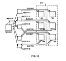
- FIG. 13 is represented a general diagram of the various connections between blocks of the switch where an optical bus BUSGMP / GCS connects the groups of packet memories to the outgoing circuit groups, an optical bus BUSMQ / RTP connects the packet transfer network to the marker and a LIGCS / MQ link connects the marker to the outgoing circuit groups.
- FIG. 14 represents the output bus BS, broken down into four buses BS07, BS815, BS1623 and BS2431, going respectively from each of the four sets of eight groups of packet memories GMPO to GMP7, GMP8 to GMP15, GMP16 to GMP23 and GMP24 to GMP31 to four access demultiplexers receiving ARGMPA, ARGMPB, ARGMPC and ARGMPD packet memory groups in each group of outgoing circuits GCSO to GCS31.
- This output bus BS sends thirty-two characteristics of new packets received CNPR in four frames of eight times a time interval divided into six packet memory address bits, five destination outgoing circuit group address bits, three destination outgoing circuit group bits, twelve packet length bits in bytes, three memory group load indicator bits packets and three bits of control and reserve.
- These two input and output buses BE and BS constitute the optical bus BUSGMP / GCS which connects the groups of packet memories to the groups of outgoing circuits.
- the LIGCS / MQ link is a set of thirty-two point-to-point links from each group of outgoing circuits to each ARCCS outgoing circuit control access reception circuit of the MQ marker ( Figure 7), on which the AEAC connect-end address signals composed of five packet memory group address bits, six packet memory address bits, five outgoing circuit group address bits, three bit outgoing circuit address, a parity bit of the AS3 access switch of the outgoing circuit, a request bit and three reserve bits.
- the asynchronous switch described above must make it possible to switch packets in the context, for example, of multiservice networks comprising video communication, that is to say with very high speeds.
Landscapes
- Engineering & Computer Science (AREA)
- Computer Networks & Wireless Communication (AREA)
- Signal Processing (AREA)
- Physics & Mathematics (AREA)
- Mathematical Physics (AREA)
- Data Exchanges In Wide-Area Networks (AREA)
Applications Claiming Priority (2)
| Application Number | Priority Date | Filing Date | Title |
|---|---|---|---|
| FR8416991 | 1984-11-08 | ||
| FR8416991A FR2572871B1 (fr) | 1984-11-08 | 1984-11-08 | Commutateur de paquets asynchrone |
Publications (1)
| Publication Number | Publication Date |
|---|---|
| EP0183592A1 true EP0183592A1 (de) | 1986-06-04 |
Family
ID=9309375
Family Applications (1)
| Application Number | Title | Priority Date | Filing Date |
|---|---|---|---|
| EP85402159A Withdrawn EP0183592A1 (de) | 1984-11-08 | 1985-11-08 | Asynchrone Paketvermittlung |
Country Status (2)
| Country | Link |
|---|---|
| EP (1) | EP0183592A1 (de) |
| FR (1) | FR2572871B1 (de) |
Cited By (13)
| Publication number | Priority date | Publication date | Assignee | Title |
|---|---|---|---|---|
| FR2606567A1 (fr) * | 1986-11-07 | 1988-05-13 | Francois Joel | Systeme de commutation de paquets |
| DE3735187A1 (de) * | 1987-10-17 | 1989-04-27 | Philips Patentverwaltung | Verfahren und schaltungsanordnung zur koppelfeldsteuerung in einem vermittlungsknoten eines breitband-vermittlungssystems |
| US4969149A (en) * | 1988-07-14 | 1990-11-06 | U.S. Philips Corporation | Switching network for a switching system |
| EP0405042A1 (de) * | 1989-06-29 | 1991-01-02 | International Business Machines Corporation | Schnelles, digitales Paketvermittlungssystem |
| EP0355797A3 (de) * | 1988-08-26 | 1991-02-06 | Hitachi, Ltd. | Signalisierungsgerät zur Verwendung in einem ATM-Vermittlungssystem |
| US5007048A (en) * | 1987-09-30 | 1991-04-09 | U.S. Philips Corporation | Circuit arrangement for avoiding overload in a wideband switching system |
| US5067124A (en) * | 1988-10-01 | 1991-11-19 | U.S. Philips Corporation | Packet switching network for a communication system |
| US5101404A (en) * | 1988-08-26 | 1992-03-31 | Hitachi, Ltd. | Signalling apparatus for use in an ATM switching system |
| US5128927A (en) * | 1987-12-23 | 1992-07-07 | U.S. Philips Corporation | Switching network and switching network control for a transmission system |
| EP0465532A4 (en) * | 1989-03-31 | 1993-05-05 | J Noel Chiappa | High speed data packet switching circuit and method |
| US5285445A (en) * | 1987-12-17 | 1994-02-08 | U.S. Philips Corporation | Switching network and switching network control for a switching node in a wideband transmission system |
| US5303236A (en) * | 1988-08-26 | 1994-04-12 | Hitachi, Ltd. | Signalling apparatus for use in an ATM switching system |
| EP0321050B1 (de) * | 1987-12-17 | 1995-03-22 | Philips Patentverwaltung GmbH | Vermittlungsknoten eines Breitband-Vermittlungssystems |
Citations (4)
| Publication number | Priority date | Publication date | Assignee | Title |
|---|---|---|---|---|
| FR2310051A1 (fr) * | 1975-04-30 | 1976-11-26 | Materiel Telephonique | Dispositif permettant l'echange d'informations numeriques entre des lignes entrantes et des lignes sortantes |
| FR2478911A1 (fr) * | 1980-03-20 | 1981-09-25 | Labo Cent Telecommunicat | Reseau a commutation de paquets, commutateur de paquets et procede d'acheminement pour un tel reseau |
| FR2513472A2 (fr) * | 1980-03-20 | 1983-03-25 | Labo Cent Telecommunicat | Commutateur de paquets pour un reseau a commutation de paquets |
| WO1984001068A1 (en) * | 1982-08-26 | 1984-03-15 | Scully Richard L | A pulse code modulated digital automatic branch exchange |
Family Cites Families (1)
| Publication number | Priority date | Publication date | Assignee | Title |
|---|---|---|---|---|
| US4512011A (en) * | 1982-11-01 | 1985-04-16 | At&T Bell Laboratories | Duplicated network arrays and control facilities for packet switching |
-
1984
- 1984-11-08 FR FR8416991A patent/FR2572871B1/fr not_active Expired
-
1985
- 1985-11-08 EP EP85402159A patent/EP0183592A1/de not_active Withdrawn
Patent Citations (4)
| Publication number | Priority date | Publication date | Assignee | Title |
|---|---|---|---|---|
| FR2310051A1 (fr) * | 1975-04-30 | 1976-11-26 | Materiel Telephonique | Dispositif permettant l'echange d'informations numeriques entre des lignes entrantes et des lignes sortantes |
| FR2478911A1 (fr) * | 1980-03-20 | 1981-09-25 | Labo Cent Telecommunicat | Reseau a commutation de paquets, commutateur de paquets et procede d'acheminement pour un tel reseau |
| FR2513472A2 (fr) * | 1980-03-20 | 1983-03-25 | Labo Cent Telecommunicat | Commutateur de paquets pour un reseau a commutation de paquets |
| WO1984001068A1 (en) * | 1982-08-26 | 1984-03-15 | Scully Richard L | A pulse code modulated digital automatic branch exchange |
Non-Patent Citations (1)
| Title |
|---|
| IEEE INTERNATIONAL CONFERENCE ON COMMUNICATIONS, vol. 3, session 3, 13-17 juin 1982, pages 5C.3.1-5C.3.5, IEEE, Philadelphia, US; FUKUYA ISHINO et al.: "A high throughput packet switching system" * |
Cited By (16)
| Publication number | Priority date | Publication date | Assignee | Title |
|---|---|---|---|---|
| EP0270471A1 (de) * | 1986-11-07 | 1988-06-08 | Joel François | Paketvermittlungssystem |
| FR2606567A1 (fr) * | 1986-11-07 | 1988-05-13 | Francois Joel | Systeme de commutation de paquets |
| US5007048A (en) * | 1987-09-30 | 1991-04-09 | U.S. Philips Corporation | Circuit arrangement for avoiding overload in a wideband switching system |
| DE3735187A1 (de) * | 1987-10-17 | 1989-04-27 | Philips Patentverwaltung | Verfahren und schaltungsanordnung zur koppelfeldsteuerung in einem vermittlungsknoten eines breitband-vermittlungssystems |
| US5285445A (en) * | 1987-12-17 | 1994-02-08 | U.S. Philips Corporation | Switching network and switching network control for a switching node in a wideband transmission system |
| EP0321050B1 (de) * | 1987-12-17 | 1995-03-22 | Philips Patentverwaltung GmbH | Vermittlungsknoten eines Breitband-Vermittlungssystems |
| US5128927A (en) * | 1987-12-23 | 1992-07-07 | U.S. Philips Corporation | Switching network and switching network control for a transmission system |
| US4969149A (en) * | 1988-07-14 | 1990-11-06 | U.S. Philips Corporation | Switching network for a switching system |
| EP0355797A3 (de) * | 1988-08-26 | 1991-02-06 | Hitachi, Ltd. | Signalisierungsgerät zur Verwendung in einem ATM-Vermittlungssystem |
| EP0355797B1 (de) * | 1988-08-26 | 1995-03-15 | Hitachi, Ltd. | Signalisierungsgerät zur Verwendung in einem ATM-Vermittlungssystem |
| US5101404A (en) * | 1988-08-26 | 1992-03-31 | Hitachi, Ltd. | Signalling apparatus for use in an ATM switching system |
| US5303236A (en) * | 1988-08-26 | 1994-04-12 | Hitachi, Ltd. | Signalling apparatus for use in an ATM switching system |
| US5067124A (en) * | 1988-10-01 | 1991-11-19 | U.S. Philips Corporation | Packet switching network for a communication system |
| EP0465532A4 (en) * | 1989-03-31 | 1993-05-05 | J Noel Chiappa | High speed data packet switching circuit and method |
| US5038343A (en) * | 1989-06-29 | 1991-08-06 | International Business Machines Corporation | High speed digital packet switching system |
| EP0405042A1 (de) * | 1989-06-29 | 1991-01-02 | International Business Machines Corporation | Schnelles, digitales Paketvermittlungssystem |
Also Published As
| Publication number | Publication date |
|---|---|
| FR2572871B1 (fr) | 1987-01-23 |
| FR2572871A1 (fr) | 1986-05-09 |
Similar Documents
| Publication | Publication Date | Title |
|---|---|---|
| EP0609137B1 (de) | Umwandlungsvorrichtung zwischen Asynchronen- und Synchronen Übertragungsverfahren | |
| EP0126196B1 (de) | Asynchrones Zeitmultiplexkoppelfeld zu Punkt-zu-Punkt-, Mehrpunkt- und Rundsendeverbindungen | |
| FR2570907A1 (fr) | Reseau et procede de commutation de paquets avec possibilite de transmission interne de paquets dans un etage | |
| FR2758036A1 (fr) | Commutateur a mode de transfert asynchrone de cellule de plusieurs canaux d'entree a plusieurs canaux de sortie | |
| JPH10511820A (ja) | 大容量atmスイッチ | |
| FR2758037A1 (fr) | Unite d'interface de ligne pour reseau de communications | |
| FR2724277A1 (fr) | Dispositif de mise en forme de trafic et appareil de communication par paquets. | |
| FR2509944A1 (fr) | Systeme de diagnostic et methode de localisation des defauts dans un reseau de commutation a commande repartie | |
| FR2572871A1 (fr) | Commutateur de paquets asynchrone | |
| EP0446827B1 (de) | Terminaleinrichtung für asynchrones Netzwerk | |
| EP0715437A1 (de) | Weglenkungsverfahren für ATM-Netz | |
| EP0612172B1 (de) | Optisch-elektronische Satellitenzentrale zur Verbindung von optischen Teilnehmerleitungen an ein ATM-Netz | |
| FR2549673A1 (fr) | Commutateur elementaire pour autocommutateur utilisant une technique de multiplexage asynchrone | |
| FR2710167A1 (fr) | Dispositf de commutation d'unités de protocole à haut débit, et procédé de commutation correspondant. | |
| FR2729040A1 (fr) | Matrice de commutation photonique | |
| CA2243440A1 (fr) | Dispositif et procede de commutation de cellules atm a groupes de connexions, et fonctions terminales d'entree et de sortie correspondantes | |
| EP0614325B1 (de) | ATM-Netz für eine Kommunikationsanlage | |
| EP0592257B1 (de) | Verfahren und Vorrichtung zur Datenübertragung zwischen Paketbetrieb-unterstützenden Einheiten im Zentrum einer Übertragungseinrichtung | |
| EP0114433A1 (de) | Fernsprechvermittlungssystem | |
| EP0091338B1 (de) | Erweiterte modulare digitale Telefonvermittlung | |
| EP0270471B1 (de) | Paketvermittlungssystem | |
| FR2524243A1 (fr) | Central telephonique numerique modulaire | |
| EP0403361A1 (de) | Verfahren und System zur Zellenvermittlung für asynchrone Zeitvielfachvermittlungen | |
| EP0091362B1 (de) | Verallgemeinerte modulare digitale Telefonvermittlung | |
| FR2515904A1 (fr) | Systeme de transmission et de commutation pour reseau local a structure de distribution en boucle et a mode de transmission par paquets. |
Legal Events
| Date | Code | Title | Description |
|---|---|---|---|
| PUAI | Public reference made under article 153(3) epc to a published international application that has entered the european phase |
Free format text: ORIGINAL CODE: 0009012 |
|
| AK | Designated contracting states |
Kind code of ref document: A1 Designated state(s): BE DE GB IT NL SE |
|
| STAA | Information on the status of an ep patent application or granted ep patent |
Free format text: STATUS: THE APPLICATION IS DEEMED TO BE WITHDRAWN |
|
| 18D | Application deemed to be withdrawn |
Effective date: 19870205 |
|
| RIN1 | Information on inventor provided before grant (corrected) |
Inventor name: DEJEAN, JACQUES HENRI Inventor name: ORIGHONI, JEAN-CLAUDE LUCIEN ARTHUR Inventor name: HENRION, MICHEL ANDRE ROBERT |