EP0184018B1 - Démodulateur pour récepteur numérique - Google Patents
Démodulateur pour récepteur numérique Download PDFInfo
- Publication number
- EP0184018B1 EP0184018B1 EP85114166A EP85114166A EP0184018B1 EP 0184018 B1 EP0184018 B1 EP 0184018B1 EP 85114166 A EP85114166 A EP 85114166A EP 85114166 A EP85114166 A EP 85114166A EP 0184018 B1 EP0184018 B1 EP 0184018B1
- Authority
- EP
- European Patent Office
- Prior art keywords
- band
- demodulator
- coefficients
- pass filter
- digital
- Prior art date
- Legal status (The legal status is an assumption and is not a legal conclusion. Google has not performed a legal analysis and makes no representation as to the accuracy of the status listed.)
- Expired - Lifetime
Links
- 230000004044 response Effects 0.000 claims description 11
- 238000005070 sampling Methods 0.000 claims description 11
- 230000005540 biological transmission Effects 0.000 claims description 4
- 238000011045 prefiltration Methods 0.000 description 12
- 230000006399 behavior Effects 0.000 description 4
- 230000008901 benefit Effects 0.000 description 4
- 238000013461 design Methods 0.000 description 4
- 230000006870 function Effects 0.000 description 4
- 230000006872 improvement Effects 0.000 description 4
- 238000004519 manufacturing process Methods 0.000 description 4
- 238000000034 method Methods 0.000 description 4
- 230000009467 reduction Effects 0.000 description 4
- 230000003044 adaptive effect Effects 0.000 description 3
- 230000008859 change Effects 0.000 description 3
- 238000011161 development Methods 0.000 description 3
- 230000018109 developmental process Effects 0.000 description 3
- 238000003860 storage Methods 0.000 description 3
- 239000000919 ceramic Substances 0.000 description 2
- 238000010586 diagram Methods 0.000 description 2
- 238000001914 filtration Methods 0.000 description 2
- 238000012545 processing Methods 0.000 description 2
- 230000006978 adaptation Effects 0.000 description 1
- 230000032683 aging Effects 0.000 description 1
- 238000006243 chemical reaction Methods 0.000 description 1
- 238000012937 correction Methods 0.000 description 1
- 230000003247 decreasing effect Effects 0.000 description 1
- 230000000694 effects Effects 0.000 description 1
- 230000002349 favourable effect Effects 0.000 description 1
- 230000007774 longterm Effects 0.000 description 1
- 230000000873 masking effect Effects 0.000 description 1
- 238000005457 optimization Methods 0.000 description 1
- 230000010363 phase shift Effects 0.000 description 1
- 230000008569 process Effects 0.000 description 1
Images



Classifications
-
- H—ELECTRICITY
- H03—ELECTRONIC CIRCUITRY
- H03D—DEMODULATION OR TRANSFERENCE OF MODULATION FROM ONE CARRIER TO ANOTHER
- H03D3/00—Demodulation of angle-, frequency- or phase- modulated oscillations
- H03D3/007—Demodulation of angle-, frequency- or phase- modulated oscillations by converting the oscillations into two quadrature related signals
-
- H—ELECTRICITY
- H03—ELECTRONIC CIRCUITRY
- H03B—GENERATION OF OSCILLATIONS, DIRECTLY OR BY FREQUENCY-CHANGING, BY CIRCUITS EMPLOYING ACTIVE ELEMENTS WHICH OPERATE IN A NON-SWITCHING MANNER; GENERATION OF NOISE BY SUCH CIRCUITS
- H03B27/00—Generation of oscillations providing a plurality of outputs of the same frequency but differing in phase, other than merely two anti-phase outputs
-
- H—ELECTRICITY
- H03—ELECTRONIC CIRCUITRY
- H03B—GENERATION OF OSCILLATIONS, DIRECTLY OR BY FREQUENCY-CHANGING, BY CIRCUITS EMPLOYING ACTIVE ELEMENTS WHICH OPERATE IN A NON-SWITCHING MANNER; GENERATION OF NOISE BY SUCH CIRCUITS
- H03B28/00—Generation of oscillations by methods not covered by groups H03B5/00 - H03B27/00, including modification of the waveform to produce sinusoidal oscillations
-
- H—ELECTRICITY
- H03—ELECTRONIC CIRCUITRY
- H03D—DEMODULATION OR TRANSFERENCE OF MODULATION FROM ONE CARRIER TO ANOTHER
- H03D2200/00—Indexing scheme relating to details of demodulation or transference of modulation from one carrier to another covered by H03D
- H03D2200/0001—Circuit elements of demodulators
- H03D2200/0035—Digital multipliers and adders used for detection
-
- H—ELECTRICITY
- H03—ELECTRONIC CIRCUITRY
- H03D—DEMODULATION OR TRANSFERENCE OF MODULATION FROM ONE CARRIER TO ANOTHER
- H03D2200/00—Indexing scheme relating to details of demodulation or transference of modulation from one carrier to another covered by H03D
- H03D2200/0041—Functional aspects of demodulators
- H03D2200/005—Analog to digital conversion
-
- H—ELECTRICITY
- H03—ELECTRONIC CIRCUITRY
- H03D—DEMODULATION OR TRANSFERENCE OF MODULATION FROM ONE CARRIER TO ANOTHER
- H03D2200/00—Indexing scheme relating to details of demodulation or transference of modulation from one carrier to another covered by H03D
- H03D2200/0041—Functional aspects of demodulators
- H03D2200/0092—Detection or reduction of fading in multipath transmission arrangements
-
- H—ELECTRICITY
- H03—ELECTRONIC CIRCUITRY
- H03D—DEMODULATION OR TRANSFERENCE OF MODULATION FROM ONE CARRIER TO ANOTHER
- H03D3/00—Demodulation of angle-, frequency- or phase- modulated oscillations
- H03D3/001—Details of arrangements applicable to more than one type of frequency demodulator
-
- H—ELECTRICITY
- H03—ELECTRONIC CIRCUITRY
- H03D—DEMODULATION OR TRANSFERENCE OF MODULATION FROM ONE CARRIER TO ANOTHER
- H03D3/00—Demodulation of angle-, frequency- or phase- modulated oscillations
- H03D3/006—Demodulation of angle-, frequency- or phase- modulated oscillations by sampling the oscillations and further processing the samples, e.g. by computing techniques
Definitions
- the invention is based on a demodulator according to the preamble of the main claim.
- a digital demodulator for frequency-modulated signals is already known from EP-A1-80 014.
- the known demodulator has a broadband analog bandpass, which is followed by an analog-digital converter.
- Low-pass filters, which filter out the actual useful signal are connected after the digital multipliers.
- the digital signals obtained in this way are processed in a subsequent circuit.
- the analog-digital converter For the analog-digital converter to work properly, however, the maximum value of the total signal must be taken as a basis, so that the analog-digital converter has to cope with this dynamic.
- analog-to-digital converters In order to be able to select weak transmitters in addition to a strong transmitter, it is necessary in the prior art to use analog-to-digital converters with a high resolution, which, however, causes difficulties in view of the fast time response required.
- the known digital demodulators are therefore insensitive to weak transmitters arranged next to strong transmitters or can only be implemented with great effort due to the effort involved in the analog-digital conversion.
- the demodulator according to the invention with the characterizing features of the main claim has the advantage that the use of narrow-band pre-filters prevents other adjacent transmitters from falling into the band of the analog pre-filter in addition to the useful signal.
- an equalizer network which eliminates the phase and attenuation distortions of the narrowband pre-filter. Since interference from strong transmitters in the vicinity of a weak transmitter cannot occur, it is possible to reduce the dynamic requirements with regard to the useful signal. The word length of the analog-digital converter can therefore be greatly reduced.
- Another advantage is that the sampling frequency of the analog-to-digital converter can be further reduced due to the smaller bandwidth of the signal to be processed.
- non-recursive filters it is also advantageous to use the non-recursive filters to suppress multipath reception. To do this, only the filter coefficients have to be adjusted accordingly depending on the phase and the strength of the reflection. A significant simplification of the non-recurring filter results when only simple reflections are considered. Then a large part of the coefficients becomes zero, so that the circuit complexity for the non-recursive filters is considerably reduced.
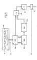
- FIG. 1 shows a digital receiver according to the invention
- FIG. 2 shows the absolute frequency response and the group delay of a commercially available ceramic filter
- FIG. 3 shows an example for the selection of the coefficients for equalizing a filter according to FIG. 2
- FIG. 4 shows a diagram to explain the improvement in the transmission behavior in FIG
- FIG. 5 shows an exemplary embodiment of a non-recursive filter
- FIG. 6 shows a simplified non-recursive filter for reducing received single reflections
- FIG. 7 shows an example for the selection of the coefficients for masking out the multipath reception signals.
- EP-A1 80 014 a digital demodulator with analog pre-filtering is provided in order to enable subharmonic sampling of the output signal of the IF stage.
- the relationships between the pre-filter bandwidth and the required sampling frequency are shown there.
- the goal is to achieve an effective reduction in the sampling frequency by using appropriately small pre-filter bandwidths, but on the other hand to assume that the analog pre-filters are sufficiently wide so that the signal to be subsequently filtered out digitally is not distorted in phase and amplitude response by the unfavorable properties of the analog filter.
- a pre-filter bandwidth is proposed here that is significantly larger than the bandwidth of the signal to be received.
- the pre-filter bandwidth is set to be significantly larger than the actual IF bandwidth, the case cannot be ruled out that a number of neighboring transmitters fall in this band in addition to the useful transmitter, which levels may be considerably higher than the useful transmitter. This is especially true if the location of reception, for example in the case of vehicles, is constantly changing. Before the signals are processed, analog-digital converters are therefore necessary which have a sufficient dynamic reserve and therefore have to process relatively large word lengths.
- the block diagram of a digital receiver with equalizer network is shown in FIG. 1.
- the analog intermediate frequency signal comes to a narrow-band filter 10 which is designed as a bandpass.
- the analog filter 10 is followed by an analog-to-digital converter 11.
- Digital multipliers 12 and 13 are connected to the digital output of the analog-to-digital converter 11, wherein in the multiplier 12 the multiplication by a cosine function by the carrier frequency fo present after the sampling while in the multiplier 13, the multiplication is carried out with a sine function of the same frequency.
- the multiplier 12 is followed by a non-recursive filter 14 and a non-recursive filter 17.
- the output of the non-recursive filter 14 leads to an adder 18, while the output of the non-recursive filter 17 leads to an adder 19.
- Two non-recursive filters 15 and 16 are likewise connected to multiplier 13, the output of the non-recursive filter 15 being connected to the further input of the adder 19 and the output of the non-recursive filter 16 being connected to a further input of the adder 18.
- the outputs of the digital adders 18 and 19 lead to an amplitude control circuit 20 which is constructed in a known manner and e.g. is described in detail in European patent application EP-A1 80014.
- the output signal of the amplitude control circuit 20 leads in one pointer to a timing element 21 and in the other branch to a timing element 22.
- the timing elements 21 and 22 each lead to a multiplier 23 and 24, to which the undelayed signal of the other branch is also fed.
- the digital output signals of the multipliers 23 and 24 lead to an adder 25, the output signal of the multiplier 23 being additively and the output signal of the multiplier 24 being supplied to the adder 25 subtractively.
- the adder 25 is followed by an arc-sine table 26.
- the low-frequency digital LF signal can be tapped at the output of the arc-sine table 26.
- the filters 14 and 15 have the impulse response er (k), while the other two recursive filters 16 and 17 have the impulse response e, (k) and -e, (k), respectively.
- Design examples for non-recursive filters can be found, for example, in the book H. W. Schüssler, Digital Systems for Signal Processing, Springer-Verlag, Berlin 1973. An example is briefly discussed below.
- the coefficients of the digital equalizers e r (k) and e, (k) must be designed so that the connection in series of the analog bandpass 10 and the equalizer has the same effect as the optimized low-pass pair alone, which in the digital receiver according to the prior art Technology is used. Since the number of equations usually exceeds the number of coefficients in the development of the equation system for the development of the coefficients, the solution must be solved in terms of a minimal square of error, ie the coefficients must be chosen so that the impulse response of the overall system is that of an optimized IF - Low pass approximated as optimally as possible.
- the solutions in the sense of a minimal square of errors are known per se and are described, for example, in the article H. Schenk, Design of Send and Receive Filters for Use in Digital Modems, Archive for Electrical Transmission No. 33, 1979, pages 425 to 431.
- FIG. 2a shows the frequency response
- FIG. 2b shows the group delay of a commercially available ceramic IF filter for use in a receiver. If the equalizing network is calculated from the determined values of the filter, the coefficient sets of the various equalizing branches are obtained, 24 coefficients being provided in the exemplary embodiment.
- FIG. 3a shows, by way of example, coefficients for the non-recursive filters 14 and 15, while FIG. 3b shows the coefficients for the non-recursive filters 16 and 17. The resulting reduction in nonlinear distortions can be seen from FIG. 4.
- the equalization that can be achieved depends on how many coefficients the optimization is carried out with.
- FIG. 3a shows the frequency response
- FIG. 2b shows the group delay of a commercially available ceramic IF filter for use in a receiver.
- FIG. 4a shows the harmonic distortion of the demodulated signal as a function of the frequency of the modulating signal at a frequency deviation of 75 kHz without using an equalizer.
- the harmonic distortion curves are compared in FIG. 4b when using equalizers with different numbers of coefficients in each branch.
- the curves for 32, 24 and 16 coefficients are shown as examples. It can be seen that an improvement can be achieved with an increasing number of coefficients, but the improvement becomes smaller and smaller with an increasing number of coefficients.
- FIG. 5 shows a non-recursive filter, as can be used for example for filters 14, 15, 16 and 17.
- the input signal E arrives at the N-stage shift register 105, each shift register location being connected to a RAM 106.
- the shift register is clocked by the input clock TE.
- the output of RAM 106 is fed to an input of a multiplier 110.
- the output of a further RAM 108 is connected to a further input of the multiplier 110.
- the addresses of RAM 106 and 108 are controlled by a PROM 107.
- the output of the multiplier 110 leads to a summer 111, which is connected as an accumulator, the output of the summer 111 leads to an output switch 112, at whose output the output signal can be tapped.
- the output switch 112 is clocked with the clock TA.
- Digital non-recursive filters are essentially characterized in that the current values and historical values are multiplied by the predetermined coefficients, the values of the coefficients being determined by the desired behavior of the filters. These multiplied values are added and are available at the output of the filter. In the case of the non-recursive filters shown in FIG. 5, the peculiarity of the scan reduction still results. With each clock pulse of the clock TE, the value present at the input of the shift register 105 is transferred to the shift register and the past value is shifted further by one. If four values are read in the exemplary embodiment, the entire content of the shift register 105 is transferred to the RAM 106 and the four memory values are stored in four specific memory locations of the RAM 106, i.e. the four oldest historical values are overwritten.
- the coefficients of the equalizer filter are not to be changed after they have been stored, they can be stored in the PROM 107. In this case, the RAM 108 is omitted. However, if a change in the coefficients for adaptive adaptation to the bandpass filter 10 is desired, it is expedient to store the coefficients in the RAM 108, since they can be changed there.
- the sum value is read into the output register 112, where it is available for further processing during a sampling clock period.
- the scan reduction is not mandatory, but is only listed here as an example. In principle, it is possible to choose the output and the input clock the same.
- the coefficients which can be seen for the exemplary embodiment in FIG. 3 can be permanently stored in the PROM 107 if the properties of the bandpass are known as such. Storage in the PROM 107 is also possible if the bandpass 10 is different, but a change in its data is not expected during the life of the demodulator. If, for example, different bandpasses are used, it is sufficient if the memory 107 of the non-recursive filters 14, 15, 16 and 17 is exchanged in order to adapt the entire circuit arrangement to different bandpasses. Furthermore, it is possible to program the memory 107 only when the bandpass 10 is already installed in the digital demodulator. This makes it possible to take individual manufacturing deviations into account even with the same band passes and to optimize the non-recursive filters accordingly.
- the data of the individual analog prefilters 10, for example the magnitude frequency and group delay, or the impulse response are read into a computer for this purpose.
- the equalizer coefficients are calculated according to the method described above and in the PROM 107, which is used in the individual digital receiver as a coefficient memory. In its present form, the method is not adaptive. However, it is also possible, by automatically recording the impulse response of the analog prefilter, for example at regular intervals or when the device is switched on, to calculate the equalizer data using a microprocessor in the device and to store the determined coefficients in RAM 108. In this way, long-term changes in the band pass 10 can also be compensated for.
- the equalization circuit arrangement described can also be used to reduce the non-linear distortions under the influence of multipath reception. To do this, only the strengths of the reflections and their phase positions and the transit time differences between the direct wave and the reflections need to be known. In this case, the transmission connector, which is disturbed by reflections, should be treated like a bandpass filter, the amplitude response and phase delay of which are fixed. The dimensioning of the non-recursive filters is then carried out in the same way as described above.
- the simplified non-recursive filter which can be used for filters 14, 15, 16 and 17, is shown in FIG.
- the input signal E reaches the shift registers 50, 51 and possibly further shift registers.
- the input signal is further fed to a multiplier 52.
- Further multipliers are connected between the shift registers, for example between the shift registers 50 and 51 the multiplier 53, after the shift register 51 the multiplier 54 and at the end of the shift register chain the multiplier 55.
- the coefficients, which are the properties of the non-recursive filter serve as a further input variable for the multipliers determine and which are stored in the memory 57.
- the outputs of the multipliers 52 to 54 are each led to an input of an adder 56, at the output of which the filtered signal can be tapped.
- the shift registers 50 and 51 and further shift registers take advantage of the property that most coefficients are 0 in the case of single reflection. The only difference from 0 are the coefficients that correspond to multiples of the transit time difference between the direct and reflecting waves divided by the sampling interval. If the shift registers 50 and 51 are therefore clocked at a certain sampling rate, then each individual delay element of the shift register chain must have so many storage locations that the sampling interval multiplied by the number of storage locations results in the runtime difference.
- the transit time difference between the direct and the reflected wave changes, this can be taken into account simply by storing or switching off memory locations 50 and 51 in the shift registers.
- the values of the coefficients themselves only depend on the strength of the reflection and its phase position. not from the runtime difference. This is only reflected in the structuring of the state memory of the equalizer as described.
- An example of the choice of the coefficients can be seen in FIG. 7. It can be seen that in the case under consideration here, in which the amplitude of the reflected wave is greater by a factor of 1.11 than that of the direct wave, the coefficients have an exponentially increasing characteristic. If the amplitude of the reflected wave is smaller than that of the direct wave, the result is an exponentially decreasing characteristic.
Landscapes
- Engineering & Computer Science (AREA)
- Power Engineering (AREA)
- Cable Transmission Systems, Equalization Of Radio And Reduction Of Echo (AREA)
- Circuits Of Receivers In General (AREA)
Claims (7)
Applications Claiming Priority (2)
| Application Number | Priority Date | Filing Date | Title |
|---|---|---|---|
| DE19843444449 DE3444449A1 (de) | 1984-12-06 | 1984-12-06 | Demodulator fuer digitale empfaenger |
| DE3444449 | 1984-12-06 |
Publications (3)
| Publication Number | Publication Date |
|---|---|
| EP0184018A2 EP0184018A2 (fr) | 1986-06-11 |
| EP0184018A3 EP0184018A3 (en) | 1988-01-20 |
| EP0184018B1 true EP0184018B1 (fr) | 1991-01-23 |
Family
ID=6252011
Family Applications (1)
| Application Number | Title | Priority Date | Filing Date |
|---|---|---|---|
| EP85114166A Expired - Lifetime EP0184018B1 (fr) | 1984-12-06 | 1985-11-07 | Démodulateur pour récepteur numérique |
Country Status (3)
| Country | Link |
|---|---|
| EP (1) | EP0184018B1 (fr) |
| JP (1) | JPS61137406A (fr) |
| DE (2) | DE3444449A1 (fr) |
Cited By (1)
| Publication number | Priority date | Publication date | Assignee | Title |
|---|---|---|---|---|
| DE4240609A1 (de) * | 1992-12-03 | 1994-06-09 | Grundig Emv | Verfahren zur Frequenzgangkorrektur |
Families Citing this family (12)
| Publication number | Priority date | Publication date | Assignee | Title |
|---|---|---|---|---|
| DE3517485A1 (de) * | 1985-05-15 | 1986-11-20 | Blaupunkt-Werke Gmbh, 3200 Hildesheim | Demodulator fuer frequenzmodulierte signale in digitaler form |
| US4829543A (en) * | 1987-12-04 | 1989-05-09 | Motorola, Inc. | Phase-coherent TDMA quadrature receiver for multipath fading channels |
| US4873683A (en) * | 1987-12-04 | 1989-10-10 | Motorola, Inc. | TDMA radio system employing BPSK synchronization for QPSK signals subject to random phase variation and multipath fading |
| US4847869A (en) * | 1987-12-04 | 1989-07-11 | Motorla, Inc. | Rapid reference acquisition and phase error compensation for radio transmission of data |
| JPH0241006A (ja) * | 1988-07-30 | 1990-02-09 | Mitsubishi Precision Co Ltd | デモジュレータ |
| DE3916426A1 (de) * | 1989-05-19 | 1990-11-22 | Blaupunkt Werke Gmbh | Autoradio mit einem digitalen entzerrernetzwerk |
| DE4104882A1 (de) * | 1991-02-18 | 1992-08-20 | Blaupunkt Werke Gmbh | Autoradio mit einer schaltungsanordnung zur analog/digital-wandlung eines zwischenfrequenzsignals |
| DE4110084A1 (de) * | 1991-03-27 | 1992-10-01 | Blaupunkt Werke Gmbh | Verfahren zur nachbarkanalunterdrueckung beim empfang frequenzmodulierter sender |
| DE4310462C2 (de) * | 1992-12-12 | 1995-06-14 | Ant Nachrichtentech | Verfahren zur Demodulation von frequenzmodulierten Signalen |
| DE4241965C1 (de) * | 1992-12-12 | 1994-05-26 | Ant Nachrichtentech | Verfahren zur Demodulation von frequenzmodulierten Signalen |
| EP0603661A1 (fr) * | 1992-12-24 | 1994-06-29 | ANT Nachrichtentechnik GmbH | Procédé de démodulation de signaux modulés en fréquence |
| WO2020161967A1 (fr) * | 2019-02-04 | 2020-08-13 | 住友電気工業株式会社 | Dispositif de détection de décharge partielle |
Family Cites Families (2)
| Publication number | Priority date | Publication date | Assignee | Title |
|---|---|---|---|---|
| DE3274936D1 (en) * | 1981-09-26 | 1987-02-05 | Bosch Gmbh Robert | Digital demodulator for frequency-modulated signals |
| DE3517485A1 (de) * | 1985-05-15 | 1986-11-20 | Blaupunkt-Werke Gmbh, 3200 Hildesheim | Demodulator fuer frequenzmodulierte signale in digitaler form |
-
1984
- 1984-12-06 DE DE19843444449 patent/DE3444449A1/de not_active Withdrawn
-
1985
- 1985-11-07 EP EP85114166A patent/EP0184018B1/fr not_active Expired - Lifetime
- 1985-11-07 DE DE8585114166T patent/DE3581507D1/de not_active Expired - Fee Related
- 1985-12-06 JP JP60273582A patent/JPS61137406A/ja active Pending
Cited By (1)
| Publication number | Priority date | Publication date | Assignee | Title |
|---|---|---|---|---|
| DE4240609A1 (de) * | 1992-12-03 | 1994-06-09 | Grundig Emv | Verfahren zur Frequenzgangkorrektur |
Also Published As
| Publication number | Publication date |
|---|---|
| EP0184018A2 (fr) | 1986-06-11 |
| DE3444449A1 (de) | 1986-06-12 |
| DE3581507D1 (de) | 1991-02-28 |
| EP0184018A3 (en) | 1988-01-20 |
| JPS61137406A (ja) | 1986-06-25 |
Similar Documents
| Publication | Publication Date | Title |
|---|---|---|
| EP0080014B1 (fr) | Démodulateur numérique pour signaux modulés en fréquence | |
| EP0201758B1 (fr) | Démodulateur numérique pour signaux modulés en fréquence | |
| EP0184018B1 (fr) | Démodulateur pour récepteur numérique | |
| DE3422828A1 (de) | Datenempfaenger fuer aufgezeichnete daten | |
| EP0691756A1 (fr) | Annuleur d'écho avec annuleur gros analogique et annuleur fin numérique | |
| DE68919909T2 (de) | Modulationseinrichtung für ein digitales Radiokommunikationssystem. | |
| DE2718087C3 (de) | Digitaldemodulator für linear amplitudenmodulierte Datensignale | |
| DE68920349T2 (de) | Anordnung zur Auslöschung von Geisterbildern. | |
| DE68910349T2 (de) | Digitales Filter mit integrierter Dezimierung. | |
| DE3044582C2 (de) | Digitaler Verstärker, insbesondere zur Verwendung in einer digitalen Fernsprech-Teilnehmerschaltung | |
| DE2920575C2 (de) | Digital-Fernmeldesystem mit mindestens einem Vierdrahtleitungsabschnitt | |
| DE69403328T2 (de) | Verfahren und vorrichtung zum filtern eines digitalen zeitsignals und anwendung für echokorrektur in einem übertragungskanal | |
| WO2004040790A1 (fr) | Dispositif et procede de traitement de symboles pilotes a des fins d'estimation de canal par filtrage passe-bas adaptatif | |
| EP0179393B1 (fr) | Egaliseur transversal de fréquence intermédiaire | |
| DE3888104T2 (de) | Analoge Schaltung für Basisband-Modem. | |
| EP0231487B1 (fr) | Autoradio avec égaliseur ayant la forme d'un filtre numérique non récursif | |
| EP1230744B1 (fr) | Dispositif de compensation d'echo dans des procedes de transmission duplex sur une ligne a deux fils | |
| DE3408384C2 (de) | Schaltkreis zur Nachbildung einer Impedanz | |
| EP0398169B1 (fr) | Autoradio avec réseau numérique d'égalisation | |
| DE19937505C2 (de) | Empfangsverfahren und Empfängeranordnung für ein Duplex-Übertragungssystem | |
| DE68908794T2 (de) | Filtervorrichtung mit sinusförmiger Flankenabrundung für die Zwischenfrequenz im Empfängerteil eines digitalen Modems. | |
| EP0444322B1 (fr) | Autoradio avec égaliseur numérique | |
| DE3532857A1 (de) | Digitales nichtrekursives filter | |
| DE4011238A1 (de) | Anordnung zur beeinflussung der uebertragungsfunktion eines datenuebertragungssystems | |
| EP1118163A1 (fr) | Filtrage d'une bande de frequences de reception |
Legal Events
| Date | Code | Title | Description |
|---|---|---|---|
| PUAI | Public reference made under article 153(3) epc to a published international application that has entered the european phase |
Free format text: ORIGINAL CODE: 0009012 |
|
| AK | Designated contracting states |
Kind code of ref document: A2 Designated state(s): DE FR NL |
|
| RAP1 | Party data changed (applicant data changed or rights of an application transferred) |
Owner name: BLAUPUNKT-WERKE GMBH |
|
| PUAL | Search report despatched |
Free format text: ORIGINAL CODE: 0009013 |
|
| AK | Designated contracting states |
Kind code of ref document: A3 Designated state(s): DE FR NL |
|
| 17P | Request for examination filed |
Effective date: 19871211 |
|
| 17Q | First examination report despatched |
Effective date: 19890804 |
|
| GRAA | (expected) grant |
Free format text: ORIGINAL CODE: 0009210 |
|
| AK | Designated contracting states |
Kind code of ref document: B1 Designated state(s): DE FR NL |
|
| ET | Fr: translation filed | ||
| REF | Corresponds to: |
Ref document number: 3581507 Country of ref document: DE Date of ref document: 19910228 |
|
| PLBE | No opposition filed within time limit |
Free format text: ORIGINAL CODE: 0009261 |
|
| STAA | Information on the status of an ep patent application or granted ep patent |
Free format text: STATUS: NO OPPOSITION FILED WITHIN TIME LIMIT |
|
| 26N | No opposition filed | ||
| PGFP | Annual fee paid to national office [announced via postgrant information from national office to epo] |
Ref country code: FR Payment date: 20011120 Year of fee payment: 17 |
|
| PGFP | Annual fee paid to national office [announced via postgrant information from national office to epo] |
Ref country code: NL Payment date: 20011128 Year of fee payment: 17 |
|
| PGFP | Annual fee paid to national office [announced via postgrant information from national office to epo] |
Ref country code: DE Payment date: 20011227 Year of fee payment: 17 |
|
| PG25 | Lapsed in a contracting state [announced via postgrant information from national office to epo] |
Ref country code: NL Free format text: LAPSE BECAUSE OF NON-PAYMENT OF DUE FEES Effective date: 20030601 |
|
| PG25 | Lapsed in a contracting state [announced via postgrant information from national office to epo] |
Ref country code: DE Free format text: LAPSE BECAUSE OF NON-PAYMENT OF DUE FEES Effective date: 20030603 |
|
| PG25 | Lapsed in a contracting state [announced via postgrant information from national office to epo] |
Ref country code: FR Free format text: LAPSE BECAUSE OF NON-PAYMENT OF DUE FEES Effective date: 20030731 |
|
| NLV4 | Nl: lapsed or anulled due to non-payment of the annual fee |
Effective date: 20030601 |
|
| REG | Reference to a national code |
Ref country code: FR Ref legal event code: ST |