EP0184420A2 - Tête d'écriture électrographique - Google Patents
Tête d'écriture électrographique Download PDFInfo
- Publication number
- EP0184420A2 EP0184420A2 EP85308773A EP85308773A EP0184420A2 EP 0184420 A2 EP0184420 A2 EP 0184420A2 EP 85308773 A EP85308773 A EP 85308773A EP 85308773 A EP85308773 A EP 85308773A EP 0184420 A2 EP0184420 A2 EP 0184420A2
- Authority
- EP
- European Patent Office
- Prior art keywords
- high voltage
- electrodes
- electrographic
- marking head
- voltage transistor
- Prior art date
- Legal status (The legal status is an assumption and is not a legal conclusion. Google has not performed a legal analysis and makes no representation as to the accuracy of the status listed.)
- Granted
Links
Images


Classifications
-
- B—PERFORMING OPERATIONS; TRANSPORTING
- B41—PRINTING; LINING MACHINES; TYPEWRITERS; STAMPS
- B41J—TYPEWRITERS; SELECTIVE PRINTING MECHANISMS, i.e. MECHANISMS PRINTING OTHERWISE THAN FROM A FORME; CORRECTION OF TYPOGRAPHICAL ERRORS
- B41J2/00—Typewriters or selective printing mechanisms characterised by the printing or marking process for which they are designed
- B41J2/385—Typewriters or selective printing mechanisms characterised by the printing or marking process for which they are designed characterised by selective supply of electric current or selective application of magnetism to a printing or impression-transfer material
- B41J2/39—Typewriters or selective printing mechanisms characterised by the printing or marking process for which they are designed characterised by selective supply of electric current or selective application of magnetism to a printing or impression-transfer material using multi-stylus heads
- B41J2/40—Typewriters or selective printing mechanisms characterised by the printing or marking process for which they are designed characterised by selective supply of electric current or selective application of magnetism to a printing or impression-transfer material using multi-stylus heads providing current or voltage to the multi-stylus head
Definitions
- This invention relates to a thin-film high-voltage electrographic writing head for recording information upon a record medium, by means of a continuous writing process.
- the writing head comprises thin-film elements including stylus electrodes, driver circuitry, and transistor switching elements integrally fabricated upon a large area substrate.
- the continuous process is implemented by an arrangement of the switching elements, including a latching circuit connected to a high voltage resistor, associated with each stylus.
- Electrographic writing systems are well known. They comprise a writing head usually having a linear array of thousands of styli for generating sequential raster lines of information by means of high voltage electrical discharges across a minute air gap to a conductive electrode.
- An insulating record medium interposed between the styli and the conductive electrode, retains thereon invisible electrostatically-charged areas formed on its surface in response to the electrical discharges. Subsequently, the charged areas are rendered visible by the application of "ink”, which may be in liquid or powder form, held to the medium by electrostatic attraction.
- the visible image may be fixed to the medium in any one of a variety of ways, to produce a permanent record.
- One common form of the electrographic writing apparatus comprises a dual electrode system, wherein the writing head styli comprise a first array of recording electrodes spaced from, and cooperating with, a second electrode comprising segmented backing electrodes.
- the writing head styli comprise a first array of recording electrodes spaced from, and cooperating with, a second electrode comprising segmented backing electrodes.
- a system is shown and described in US 2 919 171 and US 3 771 634.
- the record medium passes between the electrode arrays with a conductive layer in contact with the backing electrodes and a dielectric charge-retentive layer slightly spaced from the recording electrodes by an air gap.
- This arrangement incorporating a coincident voltage system for charging the record medium, enables simplification of the addressing scheme.
- Signal information voltages of a given polarity are applied to a selected stylus electrodes, and a supplemental addressing voltage of opposite polarity is applied to the backing electrodes. Neither the signal nor the addressing voltage is sufficient, by itself, to cause charging of the record medium. However, when the two voltages are simultaneously applied directly across the medium, the resultant total voltage is sufficient to cause an electrical discharge, or breakdown, across the air gap, for applying an electrostatic charge on the surface of the dielectric layer.
- the thousands of stylus electrodes are divided into sections, and like-numbered electrodes in each section are connected together so that all like-numbered styli, in each section, receive the same signal information voltage. A signal segmented backing electrodes is registered with each section.
- the present invention provides an electrographic marking head which is as claimed in the appended claims.
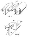
- FIG. 1 there is illustrated in Figure 1 the relevant elements of an electrographic writing system 10.
- a writing head 12 is provided for depositing an electrostatic charge image on a surface of record medium 14, in a manner which will be explained in greater detail below.
- the record medium comprises a dielectric layer 16 and a conductive layer 18.
- This configuration is but one form of the record medium, which may take other conventional forms as long as a dielectric layer is adjacent the writing head, for retaining a charge, and a conductive backing is contiguous with the dielectric layer, for completing an electrical path to a source of reference potential.
- a web of record medium 14 is paid off a supply spool 20 and is advanced in the direction of arrow 22.
- Dancer roller 24 imparts suitable tension to the web, and guide rollers 26 and 28 on either side of the writing head 12 control the proper wrap angle of the web thereover.
- the source of reference potential 30 (shown as ground) is in electrical contact with the conductive backing layer 20 through a suitable shoe 32.
- the writing head of the present invention comprises a sandwich, including a substrate 34 upon which an array of thin-film conductive stylus electrodes 36 have been fabricated, and a protective insulating overcoat 38.
- a substrate 34 upon which an array of thin-film conductive stylus electrodes 36 have been fabricated
- a protective insulating overcoat 38 At the edge of the head, in contact with the record medium, the ends of the conductive styli are exposed and are maintained slightly spaced from the surface of the medium by an air gap through which selective ionizing electrical discharges take place.
- each stylus would be about 38 ⁇ m wide, separated from the next adjacent stylus by 25 um. They may be deposited upon the substrate to a thickness in the range of 100 nm to 10 microns.
- the continuous writing process enabled by the driver electronics, allows the extremely-thin stylus electrodes to be used with improved marking results.
- the thin film fabrication technique also uniquely lends itself to much higher resolution. It should be borne in mind that the conventional electrographic writing methods, which write discontinuously, require stylus electrodes having approximately a 1:1 aspect ration (usually several tens of ⁇ m thick) in order to provide sufficient overlap of marks from line to line, as the record medium advances.
- Writing head 12 is extremely inexpensive to manufacture since all its elements are integrally fabricated upon substrate 34 (schematically shown in Figure 3) by standard thin-film deposition processes.
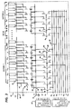
- Each stylus 36 has associated therewith a high voltage thin-film transistor 40, a thin-film load resistor 41, and a low voltage thin-film transistor 42.
- Writing data are loaded via multiplexed driver circuit incorporating address bus lines (A) 44 and data bus lines (D) 46.
- amorphous semiconductor materials such as amorphous silicon (a-Si: H) are uniquely suited to the desired operational and fabrication characteristics of the high voltage as well as the low voltage transistors.
- a-Si: H amorphous silicon
- the invention embraces a circuit which incorporates high voltage thin-film transistors (of the type identified in the preceding paragraph) and latching means, one associated with each stylus, for applying writing signals to the associated stylus electrode and for continuously holding the charge on the stylus until it is switched.
- the principle of operation of the high voltage thin-film transistor 40 relies upon the flow of charge carriers through a charge carrier transport layer 48 from a contiguous source electrode 50 to a laterally-offset drain electrode 52, also contiguous to the transport layer, under the control of a gate electrode 54.
- the gate electrode and the source electrode are aligned with one another on the opposite sides of the transport layer and the gate electrode is spaced from the transport layer by dielectric layer 55.
- the latching means for the high voltage thin-film transistor 40 is the low voltage thin-film transistor 42.
- Gate electrode 54 of the high voltage thin-film transistor 40 is connected to the drain electrode 56 of the low voltage thin-film transistor 42 whose gate electrode 58 is connected to address bus line 44, and whose source electrode 60 is connected to data bus line 46.
- signal information imposed upon the data lines, selectively latches the high voltage transistors.
- the number of address bus lines and data bus lines is reduced to a minimum through a multiplexing scheme which results in minimizing the required number of wire bonds to the external world. Wire bonds are necessary only between external IC address bus drivers 62 and the address bus lines 44, and between the external IC data bus drivers 64 and the data bus lines 46.
- the address bus lines 44 are sequentially energized. For example, when an activating signal is applied to A m , i.e. the m th (1 ⁇ m ⁇ p) address bus line, a potential, on the order of 5 to 40 volts, is applied to each of the low voltage transistor gate electrodes 53 through 58 connected thereto, for turning ON (conducting condition) every one of th e q low voltage switches in the m th section. The low voltage switches of all of the other set ie ns remain OFF (non-conducting condition). Thus, the signal information on data lines C D will pass through the low voltage transistors in the m th section to the gate electrod ; 4 of the high voltage transistors 40 in the m th section.
- a number of thin-film shift registers 66 may be integrally formed on the head substrate 34.
- the shift registers, including transistors, may also be fabricated of amorphous semiconductor materials.
- a single shift register having a number of stages coincident with the number of styli (e.g. on the order of 3000 to 4000 for a 275 mm wide head), would be employed.
- a more practical implementation would include several smaller shift registers, each having fewer stages, with a data line 68 connected to each.
- Data are fed to each shift register, in parallel and shifted from stage to stage by clock pulses delivered by common clock lines 70.
- a strobe line 72 is connected to all the gates 58 of the low voltage transistors. Once the data have been loaded into all the stages of the shift register, a strobe pulse simultaneously turns ON all the low voltage switches for loading an entire line of data, through the low voltage transistors, to latch the gate electrodes 54 of the high voltage transistors 40. It can be seen that the high voltage transistors 40 are latched for a full line writing time, i.e. between one strobe pulse and the next.
- This information-loading embodiment has several advantages over the multiplexing scheme, namely, it allows a considerable reduction of data line crossovers, it further reduces the number of wire bonds to the external world, and it allows the head to be more compact.
- the source electrodes 50 of each are connected to a reference potential 76, such as ground, through a ground bus (G) 78, and the drain electrodes 52 are connected via suitable load resistors 41 to a high voltage bus (HV) 80.
- Styli 36 are connected to the drain electrode of the high voltage transistor 40.
- Data potentials of 0 volts (OFF) or 10 to 40 volts (ON) will pass from the data bus lines 46 ( Figure 3) or 74 ( Figure 5) through the low voltage transistors to the gate electrodes of the high voltage transistors. The charge is stored in the gate capacitance of the high voltage transistor and, because of the very low leakage current of the low voltage transistor, will remain substantially unchanged until readdressed by the low voltage transistor.
- the circuit, illustrated and described represents an inverter stage, causing writing to occur when the high voltage transistor is in its OFF state, it is within the purview of this invention for the head to mark in the opposite (i.e. ON), state of the high voltage transistor.
- the arrangement illustrated in Figure 6 may be used.
- a high voltage back electrode 82 is in contact with the record medium 14 and extends fully thereacross in opposition to the writing head.
- the record medium is shown slightly spaced from the electrode array, as is conventional in this marking method.
- Electrode 82 is connected to a high voltage source 84, on the order of 600 volts.
- High voltage thin-film transistors 40 have their drain electrodes 52 connected to the styli, their source electrodes 50 connected to ground bus 86, and their gate electrodes 54 connected to latching circuits such as low voltage thin-film transistors 44 controlled by strobe bus 72. Although this embodiment has been described relative to the information-loading scheme shown in Figure 5, scheme shown in Figure 3, or any other comparable one, may be used.
- a stylus will write when the high voltage transistor is turned ON and serves as a current sink from the high voltage electrode through the air gap to ground.
- the high voltage transistor is turned OFF, no current will flow and consequently no writing will occur because no air gap discharge can be sustained.
- Signal information is loaded onto the gates 54 of the high voltage transistors 40 to control the writing (or non-writing) state of the stylus electrodes and will remain in that state until it is subsequently addressed for controlling the state of the electrodes for the writing of the next line.
- latching the high voltage transistor allows writing (or non-writing) to be effected continuously until the gate signal is changed and, therefore, thin-film styli which are inexpensive to fabricate can be used. This represents a significant improvement over conventional electrographic writing heads wherein writing takes place only while the stylus is being addressed.
- Stylus electrodes may be integrated with the desired circuit elements, such as bus lines, shift registers, active and passive devices, and all the elements may be fabricated by standard thin-film deposition techniques upon inexpensive, large area, substrate materials such as glass, ceramics and possibly some printed circuit board materials.
- the manufacturing method enables the integrated head to be cheaper, and have a higher resolution, than conventional electrographic writing heads.
- the thin-film styli are uniquely compatible with the continuous writing process described above.
Landscapes
- Printers Or Recording Devices Using Electromagnetic And Radiation Means (AREA)
- Facsimile Heads (AREA)
- Golf Clubs (AREA)
- Supporting Of Heads In Record-Carrier Devices (AREA)
- Photoreceptors In Electrophotography (AREA)
- Dot-Matrix Printers And Others (AREA)
- Electrophotography Using Other Than Carlson'S Method (AREA)
- Details Or Accessories Of Spraying Plant Or Apparatus (AREA)
- Soil Working Implements (AREA)
Priority Applications (1)
| Application Number | Priority Date | Filing Date | Title |
|---|---|---|---|
| AT85308773T ATE52458T1 (de) | 1984-12-04 | 1985-12-03 | Elektrographischer schreibkopf. |
Applications Claiming Priority (2)
| Application Number | Priority Date | Filing Date | Title |
|---|---|---|---|
| US678146 | 1984-12-04 | ||
| US06/678,146 US4588997A (en) | 1984-12-04 | 1984-12-04 | Electrographic writing head |
Publications (3)
| Publication Number | Publication Date |
|---|---|
| EP0184420A2 true EP0184420A2 (fr) | 1986-06-11 |
| EP0184420A3 EP0184420A3 (en) | 1986-11-12 |
| EP0184420B1 EP0184420B1 (fr) | 1990-05-09 |
Family
ID=24721585
Family Applications (1)
| Application Number | Title | Priority Date | Filing Date |
|---|---|---|---|
| EP85308773A Expired - Lifetime EP0184420B1 (fr) | 1984-12-04 | 1985-12-03 | Tête d'écriture électrographique |
Country Status (9)
| Country | Link |
|---|---|
| US (1) | US4588997A (fr) |
| EP (1) | EP0184420B1 (fr) |
| JP (1) | JPH0761116B2 (fr) |
| CN (1) | CN1004254B (fr) |
| AT (1) | ATE52458T1 (fr) |
| BR (1) | BR8506034A (fr) |
| DE (1) | DE3577528D1 (fr) |
| ES (1) | ES8700154A1 (fr) |
| MX (1) | MX160185A (fr) |
Families Citing this family (18)
| Publication number | Priority date | Publication date | Assignee | Title |
|---|---|---|---|---|
| CH677340A5 (fr) * | 1987-01-06 | 1991-05-15 | Pitney Bowes Inc | |
| US4766450A (en) * | 1987-07-17 | 1988-08-23 | Xerox Corporation | Charging deposition control in electrographic thin film writting head |
| EP0395448A3 (fr) * | 1989-04-28 | 1991-08-21 | Nippon Steel Corporation | Tête d'impression électrostatique |
| US5218382A (en) * | 1989-04-28 | 1993-06-08 | Synergy Computer Graphics Corporation | Electrostatic printer head structure and styli geometry |
| US4954839A (en) * | 1989-07-24 | 1990-09-04 | Cryptek, Inc. | Self-aligning print head assembly with advanced shielding characteristics |
| CA2027440C (fr) * | 1989-11-08 | 1995-07-04 | Nicholas K. Sheridon | Affichage informatique sur feuille et systeme de balayage connexe |
| US5274401A (en) * | 1990-04-27 | 1993-12-28 | Synergy Computer Graphics Corporation | Electrostatic printhead |
| US5237346A (en) * | 1992-04-20 | 1993-08-17 | Xerox Corporation | Integrated thin film transistor electrographic writing head |
| US5166960A (en) * | 1992-04-20 | 1992-11-24 | Xerox Corporation | Parallel multi-phased a-Si shift register for fast addressing of an a-Si array |
| US5337080A (en) * | 1993-04-27 | 1994-08-09 | Xerox Corporation | Amorphous silicon electrographic writing head assembly with protective cover |
| US6100909A (en) * | 1998-03-02 | 2000-08-08 | Xerox Corporation | Matrix addressable array for digital xerography |
| US6064410A (en) * | 1998-03-03 | 2000-05-16 | Eastman Kodak Company | Printing continuous tone images on receivers having field-driven particles |
| JP3396454B2 (ja) * | 1999-12-28 | 2003-04-14 | 株式会社千葉精密 | 可動磁石形検流計 |
| US6707479B1 (en) | 2003-01-14 | 2004-03-16 | Hewlett-Packard Development Company, L.P. | Apparatus and methods of printing on an electrically writable medium |
| US6982734B2 (en) * | 2003-10-06 | 2006-01-03 | Hewlett-Packard Development Company, L.P. | Printing on electrically writable media and electrically writable displays |
| US7755654B2 (en) * | 2006-07-25 | 2010-07-13 | Hewlett-Packard Development Company, L.P. | Pixel |
| US20110298760A1 (en) | 2010-06-02 | 2011-12-08 | Omer Gila | Systems and methods for writing on and using electronic paper |
| EP3100111B1 (fr) | 2014-01-31 | 2020-01-22 | Hewlett-Packard Development Company, L.P. | Dispositif d'affichage |
Family Cites Families (10)
| Publication number | Priority date | Publication date | Assignee | Title |
|---|---|---|---|---|
| US4181912A (en) * | 1977-05-12 | 1980-01-01 | Ricoh Co., Ltd. | Electrostatic recording apparatus comprising improved electrode switching means |
| US4145697A (en) * | 1977-12-28 | 1979-03-20 | Honeywell Inc. | Graphic recording apparatus with stylus addressing by shift registers |
| US4215355A (en) * | 1978-11-24 | 1980-07-29 | Gould Inc. | Improved electrographic recording apparatus employing an improved drive circuit |
| IT1118924B (it) * | 1979-07-20 | 1986-03-03 | Olivetti & Co Spa | Testina di sorittura a punti per stampanti ad alta definizione e relativo metodo di fabbricazione |
| JPS5779763A (en) * | 1980-11-06 | 1982-05-19 | Sony Corp | Drive method of thermo-sensing picture display device |
| JPS57203573A (en) * | 1981-06-10 | 1982-12-13 | Fuji Xerox Co Ltd | Thermal head |
| AU567487B2 (en) * | 1982-01-25 | 1987-11-26 | Sony Corporation | Thermal printer |
| US4472723A (en) * | 1982-04-23 | 1984-09-18 | Oki Electric Industry Co., Ltd. | Thermal head |
| JPS5979767A (ja) * | 1982-10-29 | 1984-05-09 | Fuji Xerox Co Ltd | 静電記録ヘツド |
| JPS5979769A (ja) * | 1982-10-29 | 1984-05-09 | Fuji Xerox Co Ltd | 静電記録ヘツド |
-
1984
- 1984-12-04 US US06/678,146 patent/US4588997A/en not_active Expired - Lifetime
-
1985
- 1985-11-27 JP JP60267070A patent/JPH0761116B2/ja not_active Expired - Fee Related
- 1985-11-27 ES ES549343A patent/ES8700154A1/es not_active Expired
- 1985-11-28 MX MX765A patent/MX160185A/es unknown
- 1985-12-03 EP EP85308773A patent/EP0184420B1/fr not_active Expired - Lifetime
- 1985-12-03 CN CN85108819.8A patent/CN1004254B/zh not_active Expired
- 1985-12-03 AT AT85308773T patent/ATE52458T1/de not_active IP Right Cessation
- 1985-12-03 DE DE8585308773T patent/DE3577528D1/de not_active Expired - Fee Related
- 1985-12-03 BR BR8506034A patent/BR8506034A/pt not_active IP Right Cessation
Also Published As
| Publication number | Publication date |
|---|---|
| ATE52458T1 (de) | 1990-05-15 |
| EP0184420B1 (fr) | 1990-05-09 |
| ES549343A0 (es) | 1986-10-01 |
| EP0184420A3 (en) | 1986-11-12 |
| JPS61167269A (ja) | 1986-07-28 |
| CN85108819A (zh) | 1986-07-23 |
| JPH0761116B2 (ja) | 1995-06-28 |
| ES8700154A1 (es) | 1986-10-01 |
| MX160185A (es) | 1989-12-21 |
| BR8506034A (pt) | 1986-08-19 |
| US4588997A (en) | 1986-05-13 |
| CN1004254B (zh) | 1989-05-17 |
| DE3577528D1 (de) | 1990-06-13 |
Similar Documents
| Publication | Publication Date | Title |
|---|---|---|
| EP0184420B1 (fr) | Tête d'écriture électrographique | |
| EP0172015B1 (fr) | Appareil marqueur et procédé pour les systèmes de formation d' image par projection utilisant un jet fluidique | |
| US5274401A (en) | Electrostatic printhead | |
| US5627561A (en) | Electrophoretic display panel with selective character addressability | |
| US5066946A (en) | Electrophoretic display panel with selective line erasure | |
| EP0146231B1 (fr) | Adressage de dispositifs d'affichage à cristaux liquides | |
| US4884079A (en) | Image forming apparatus and driving method therefor | |
| US6100909A (en) | Matrix addressable array for digital xerography | |
| JPS6352379B2 (fr) | ||
| US6291925B1 (en) | Apparatus and methods for reversible imaging of nonemissive display systems | |
| JPH0218590A (ja) | 垂直ライン幅制御式イオノグラフィックシステム | |
| US3732573A (en) | Electrographic printer matrix circuit | |
| US4719481A (en) | Electrographic ion writing head driver system | |
| US4424522A (en) | Capacitive electrostatic stylus writing with counter electrodes | |
| US4823284A (en) | High speed VLSI based serial to multiplexed data translator | |
| US4812860A (en) | Heater for ionographic marking head array | |
| US5717449A (en) | Toner projection printer with improved address electrode structure | |
| EP0752318B1 (fr) | Imprimante de protection de toner avec structure d'électrodes de commande à couplage capacitif | |
| US4699469A (en) | Liquid crystal display | |
| US4951071A (en) | Resistive nib ionographic imaging head | |
| Tuan | Printing applications of a-Si thin film transistors | |
| JPH0436369B2 (fr) | ||
| JPS61154955A (ja) | 熱式印刷装置 | |
| JPH1178104A (ja) | 記録ヘッド並びに画像形成装置 | |
| EP0680827B1 (fr) | Tête d'impression électrostatique |
Legal Events
| Date | Code | Title | Description |
|---|---|---|---|
| PUAI | Public reference made under article 153(3) epc to a published international application that has entered the european phase |
Free format text: ORIGINAL CODE: 0009012 |
|
| AK | Designated contracting states |
Kind code of ref document: A2 Designated state(s): AT BE DE FR GB IT NL SE |
|
| PUAL | Search report despatched |
Free format text: ORIGINAL CODE: 0009013 |
|
| AK | Designated contracting states |
Kind code of ref document: A3 Designated state(s): AT BE DE FR GB IT NL SE |
|
| RHK1 | Main classification (correction) |
Ipc: B41J 3/08 |
|
| 17P | Request for examination filed |
Effective date: 19870511 |
|
| 17Q | First examination report despatched |
Effective date: 19881205 |
|
| GRAA | (expected) grant |
Free format text: ORIGINAL CODE: 0009210 |
|
| AK | Designated contracting states |
Kind code of ref document: B1 Designated state(s): AT BE DE FR GB IT NL SE |
|
| REF | Corresponds to: |
Ref document number: 52458 Country of ref document: AT Date of ref document: 19900515 Kind code of ref document: T |
|
| REF | Corresponds to: |
Ref document number: 3577528 Country of ref document: DE Date of ref document: 19900613 |
|
| ET | Fr: translation filed | ||
| ITF | It: translation for a ep patent filed | ||
| PLBE | No opposition filed within time limit |
Free format text: ORIGINAL CODE: 0009261 |
|
| STAA | Information on the status of an ep patent application or granted ep patent |
Free format text: STATUS: NO OPPOSITION FILED WITHIN TIME LIMIT |
|
| 26N | No opposition filed | ||
| ITTA | It: last paid annual fee | ||
| EAL | Se: european patent in force in sweden |
Ref document number: 85308773.2 |
|
| PGFP | Annual fee paid to national office [announced via postgrant information from national office to epo] |
Ref country code: AT Payment date: 20001212 Year of fee payment: 16 |
|
| PG25 | Lapsed in a contracting state [announced via postgrant information from national office to epo] |
Ref country code: AT Free format text: LAPSE BECAUSE OF NON-PAYMENT OF DUE FEES Effective date: 20011203 |
|
| REG | Reference to a national code |
Ref country code: GB Ref legal event code: IF02 |
|
| PGFP | Annual fee paid to national office [announced via postgrant information from national office to epo] |
Ref country code: GB Payment date: 20021127 Year of fee payment: 18 |
|
| PGFP | Annual fee paid to national office [announced via postgrant information from national office to epo] |
Ref country code: SE Payment date: 20021204 Year of fee payment: 18 |
|
| PGFP | Annual fee paid to national office [announced via postgrant information from national office to epo] |
Ref country code: DE Payment date: 20021205 Year of fee payment: 18 |
|
| PGFP | Annual fee paid to national office [announced via postgrant information from national office to epo] |
Ref country code: FR Payment date: 20021210 Year of fee payment: 18 |
|
| PGFP | Annual fee paid to national office [announced via postgrant information from national office to epo] |
Ref country code: NL Payment date: 20021227 Year of fee payment: 18 |
|
| PGFP | Annual fee paid to national office [announced via postgrant information from national office to epo] |
Ref country code: BE Payment date: 20030218 Year of fee payment: 18 |
|
| PG25 | Lapsed in a contracting state [announced via postgrant information from national office to epo] |
Ref country code: GB Free format text: LAPSE BECAUSE OF NON-PAYMENT OF DUE FEES Effective date: 20031203 |
|
| PG25 | Lapsed in a contracting state [announced via postgrant information from national office to epo] |
Ref country code: SE Free format text: LAPSE BECAUSE OF NON-PAYMENT OF DUE FEES Effective date: 20031204 |
|
| PG25 | Lapsed in a contracting state [announced via postgrant information from national office to epo] |
Ref country code: BE Free format text: LAPSE BECAUSE OF NON-PAYMENT OF DUE FEES Effective date: 20031231 |
|
| BERE | Be: lapsed |
Owner name: *XEROX CORP. Effective date: 20031231 |
|
| PG25 | Lapsed in a contracting state [announced via postgrant information from national office to epo] |
Ref country code: NL Free format text: LAPSE BECAUSE OF NON-PAYMENT OF DUE FEES Effective date: 20040701 Ref country code: DE Free format text: LAPSE BECAUSE OF NON-PAYMENT OF DUE FEES Effective date: 20040701 |
|
| GBPC | Gb: european patent ceased through non-payment of renewal fee |
Effective date: 20031203 |
|
| EUG | Se: european patent has lapsed | ||
| PG25 | Lapsed in a contracting state [announced via postgrant information from national office to epo] |
Ref country code: FR Free format text: LAPSE BECAUSE OF NON-PAYMENT OF DUE FEES Effective date: 20040831 |
|
| NLV4 | Nl: lapsed or anulled due to non-payment of the annual fee |
Effective date: 20040701 |
|
| REG | Reference to a national code |
Ref country code: FR Ref legal event code: ST |