EP0184494A1 - System zur gleichzeitigen Übertragung von Datenblöcken oder Vektoren zwischen einem Speicher und einem oder mehreren Datenverarbeitungseinheiten - Google Patents
System zur gleichzeitigen Übertragung von Datenblöcken oder Vektoren zwischen einem Speicher und einem oder mehreren Datenverarbeitungseinheiten Download PDFInfo
- Publication number
- EP0184494A1 EP0184494A1 EP85402242A EP85402242A EP0184494A1 EP 0184494 A1 EP0184494 A1 EP 0184494A1 EP 85402242 A EP85402242 A EP 85402242A EP 85402242 A EP85402242 A EP 85402242A EP 0184494 A1 EP0184494 A1 EP 0184494A1
- Authority
- EP
- European Patent Office
- Prior art keywords
- memory
- data
- banks
- physical
- logical
- Prior art date
- Legal status (The legal status is an assumption and is not a legal conclusion. Google has not performed a legal analysis and makes no representation as to the accuracy of the status listed.)
- Granted
Links
Images


Classifications
-
- G—PHYSICS
- G06—COMPUTING OR CALCULATING; COUNTING
- G06F—ELECTRIC DIGITAL DATA PROCESSING
- G06F13/00—Interconnection of, or transfer of information or other signals between, memories, input/output devices or central processing units
- G06F13/14—Handling requests for interconnection or transfer
- G06F13/16—Handling requests for interconnection or transfer for access to memory bus
- G06F13/1605—Handling requests for interconnection or transfer for access to memory bus based on arbitration
- G06F13/1652—Handling requests for interconnection or transfer for access to memory bus based on arbitration in a multiprocessor architecture
- G06F13/1663—Access to shared memory
-
- G—PHYSICS
- G06—COMPUTING OR CALCULATING; COUNTING
- G06F—ELECTRIC DIGITAL DATA PROCESSING
- G06F12/00—Accessing, addressing or allocating within memory systems or architectures
- G06F12/02—Addressing or allocation; Relocation
- G06F12/0207—Addressing or allocation; Relocation with multidimensional access, e.g. row/column, matrix
Definitions
- the present invention relates to a system for the simultaneous transmission of data blocks or vectors between a memory and one or more data processing units.
- It relates more particularly to systems in which the data processing units operate and execute programs asynchronously with respect to each other.
- SIMD mode which is the abbreviation of the Anglo-Saxon designation "Single Instruction, Multiple Data Stream”
- SIMD mode which is the abbreviation of the Anglo-Saxon designation "Single Instruction, Multiple Data Stream”
- the data exchanges are done in synchronous mode, a single instruction timing all the elementary processors.
- the performance increase is obtained by making execute by a high number of processing units the same instruction so that it is possible with the machines carried out according to the SIMD mode to work not on scalars but on vectors or tables of data, a single instruction can for example carry out operations on sequences of numbers belonging to an array.
- MIMD mode which is the abbreviation of the Anglo-Saxon term “Multiple Instruction, Multiple Data Stream”
- MIMD mode the increase in performance is obtained by having several instructions belonging to different programs executed by different processing units, these instructions being executed simultaneously and operating on different data.
- Systems operating in MIMD mode present many implementation difficulties which lie in the resolution of conflicts of access to shared data. between all the processing units, at the level of efficient management of resources, synchronization mechanisms to be implemented, and at the level of management of concurrent processing tasks. These difficulties naturally lead to a significant drop in performance.
- SIMD and MIMD may seem complementary, the opposition between these two techniques reveals a contradiction between the possibility offered by the first system to increase the data throughput and that offered by the second system which allows maximum number of executable instructions.
- MIMD system would make it possible to derive the greatest benefit from the parallel execution of a program if there were no conflicts between the accesses to the common memory shared by the processing units.
- SIMD systems which appear more rigid at the level of the sequence of instructions, because only identical operations can be executed simultaneously, take advantage of this apparent constraint to more effectively parallelize access to the data.
- the object of the invention is to limit the aforementioned drawbacks. It notably makes it possible to avoid memory access conflicts in an MIMD organization in which each processor could operate in SIMD mode.
- the subject of the invention is a system for the simultaneous transmission of data blocks or vectors between a memory and one or more data processing units in which the data processing units operate asynchronously one compared to the others, characterized in that the memory is composed of an integer N of logical storage banks each having an integer n of any physical banks of q storage locations, the system comprising an interconnection network interposed between the memory and the units for establishing connections between the memory banks and the processing units, a logic control device for controlling the connection paths in the connection network as well as one or more logic addressing devices controlled respectively by a data processing unit for address the locations of the memory to which each unit requests access and execute the transfer by blocks of the data contained in the corresponding locations, the Nn physical banks of the memory are juxtaposed and numbered in the order of the natural numbers 0, ..
- each logical addressing device comprising means for determining the address of the physical bank in the what is each location by calculating the modulo (Nn) address of its physical bench from its serial number in the memory
- the logic control device comprising means for establishing a connection of a requesting processing unit on the logical bank containing the address of the start of the data block to be transferred and switching means for successively switching the requesting unit to the following logical banks at the end of each data transfer between a logical bank of the memory and the data processing unit.
- the advantage of the present invention is that it makes it possible to establish the connections of all the processing units simultaneously and without conflict. Once the processing unit connection has been established, the transfer of an entire data block or vector continues without interruption until the transfer of the last data item of the block or vector. Also the arrangement of the system according to the invention has the advantage of maximizing the use of all the physical banks of the memory, which makes it possible to make the interconnection network work with a constant data rate.
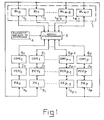
- the data transmission system represented in FIG. 1 comprises a memory 1, represented inside a closed line in dotted lines which is divided into N logical banks BL O , BL 1 .... BL n-2 , BL n-1 represented inside rectangles noted respectively from 1 0 to 1 N-1 .
- the system represented also includes a set of P + 1 data processing units denoted respectively PCUO, PCU1 etc ... PCU p-1 and PCU represented inside rectangles respectively bearing the references of 2 0 , 2 1 ,. .. 2 p-1 , 2 p .
- An interconnection network 3 establishes the connections between the processing units 2 0 to 2 p and the logic benches 1 0 to 1 N-1 .
- the interconnection network 3 is controlled from a control logic 4.
- Address processors respectively denoted PA 0 , PA 1 etc ...
- PA p-1 , PA p and bearing the references 5 0 to 5p are linked to the addressing inputs of memory 1 to allow the calculation of the address of each element to be extracted from the banks of memory 1.
- Devices for rearranging the extracted data designated respectively by COMI 0 , COMI I, etc.
- COMI p-1 , COMI p inside rectangles numbered from 6 0 to 6p are interposed between the interconnection network 3 and the processing units PCU 0 , PCU 1 to PCU p to rearrange the data extracted from memory 1 in the order in which they were recorded in memory 1 .
- the division of the memory 1 into logical banks makes it possible to obtain the parallelism of access of all the processing units to the memory storage banks.
- This parallelism is obtained thanks to the interconnection network which connects at an instant given each logical bench to a single processing unit.
- Each logical bank can however contain a number n of physical “pipeline” banks which allows each logical bank to store n words or consecutive data inside these n physical banks.
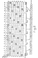
- An example of sharing a memory space into physical banks and logical banks is shown in Figure 2.
- the memory space 1 which is represented in FIG. 2 in the form of a matrix of 25 xq storage locations placed at the intersections of 25 columns and of q rows L 0 to L q-1 , is materialized by 25 benches of q juxtaposed memory locations.
- Each line has 25 memory locations numbered in order of an arithmetic progression of reason 1, the number of each location marking the beginning of a line being obtained from the last number of the location marking the end of the line previous increased by one.
- Line L 0 contains the locations numbered from 0 to 24, line L 1 which follows contains the locations numbered from 25 to 49 etc ... and the last line L q-1 contains the locations numbered from 25 (q-1 ) at 25 q-1.
- a processing unit wishes to extract from the memory space all the "articles" or "data” contained in the locations of the memory whose numbers are multiples of 7 starting with the article or the data of n ° 0.
- the processing unit must first connect to the bench BL O where the first article of n ° 0 is located then successively on the following logical benches BL to BL 4 to extract all the multiple articles of 7 whose numbers are represented surrounded by a small circle in figure 2.
- the processing unit will extract, in order, the first elements or articles supplied by each physical bench, ie the series of articles or data corresponding to the numbered locations 0, 126, 77, 28, 154 ... 98 and 49.
- the processing unit leaves the logic bench BL 4 to return by circular permutation to a new reading of the logic bench BL O then successively on the logic benches BL 1 , BL 2 , BL 3 and BL 4 to extract during this second round , the articles or data located at the locations numbered 175, 301, 252, 203, 329 ... 273 and 224.
- the vector extracted from memory is composed by a series of vectors or scalars whose sequence of addresses in memory follows an arithmetic progression verifying the relation in which A k , A o , k and R respectively denote the address of the k th article or of the k th given inside the vector, Ao the address of the start of the first article or of the first datum of the vector, k the rank or order number of the article or data in the vector and R the reason.
- a k , A o , k and R respectively denote the address of the k th article or of the k th given inside the vector
- Ao the address of the start of the first article or of the first datum of the vector
- k the rank or order number of the article or data in the vector
- R the reason.
- FIG. 3 shows examples of connection path established by a connection network capable of connecting several processing units referenced respectively by the letters A, B , C, D, E, F, G indifferently on 7 logical banks of a memory noted respectively 0, 1, 2, 3, 4, 5 and 6.
- the processing units A and C are connected to time t respectively on logic banks 0 and 3.
- the processing unit B requests access to logic bank 0 while the processing unit A is connected to logic bench 1 and processing unit C is connected to the following logic bench 4.
- a first access rule consists in considering that a processing unit already engaged in the "turnstile" is necessarily priority on the logical bench which it occupies compared to other units wanting to enter the turnstile by the same logic bench.
- a second access rule consists when at least two processing units want to have access to the same logical bench to grant this access first to the most priority unit, by naturally defining the form which this priority will have to take for each particular configuration. of the system.
- a third access rule consists in satisfying the access requests which are not conflicting simultaneously.
- each memory location can only be identified or addressed at the intersection of a row and a column of the matrix and as in the system block addressing system used by the invention
- the memory locations containing the data or items of each vector or data block are known only by addresses verifying an arithmetic progression of the address of memory locations located along each line of the memory, each address processor 5 to 5p of the transmission system according to the invention responsible for converting the addresses in arithmetical progression of the vectors known by each processing unit, into an address designating for each data or item to extract the physical bench which contains it and its location in the physical bench.
- each address processor The consequently important role of each address processor is to carry out with each new extraction of data or articles in memory the rapid division of the number of the first article or the first given by the modulo of the number of physical banks.
- a single division appears necessary for the initialization of the extraction because in the following simple additions are sufficient for the extraction of the following data or articles. Indeed, by designating by x and y the numbers of two elements or articles to be extracted from the same vector or block, and assuming that they are stored in the same physical bank of a memory with 25 physical banks, these numbers check relationships a being a positive natural integer.
- the process then consists in cutting each complete migration into subsets treated identically. For each subset processed, a calculation is carried out to know the number of the physical bank on which the migration begins, the start of transfer address for each physical bank, and the addressing step between two consecutive accesses on the same bank. From the physical bank number at the start of the transfer and the addressing step, a calculation also makes it possible to determine the address for the start on each bank, ie Adx, this calculation being done locally on each bank by an address processor. .
- Each address processor connected to each logical bank satisfies the migration request autonomously with synchronizations at the start of each subset, if there are any.
- the extracted data must then be exchanged in the logical order of organization of the tables extracted from the memory.
- a migration always begins with the execution tion, by the processing unit performing this migration, of a preliminary phase of splitting the request into a subset SE i of address elements defined by a relation of the form
- the processing unit determines the reason R, the number K max and the amplitude has jumps between two consecutive subsets SE. and SE i + 1
- the amplitude of the jumps a being defined by the relation
- the migration is broken down into three distinct phases, an initialization phase (I), a transfer phase (T) and a scheduling phase (0). Depending on the direction of the transfer, these phases do not take place in the same order. For a migration from memory 1 to a processing unit they take place in the order (I) - (T) - (0) and for a migration in the direction of processing unit to memory 1 they take place in the direction (lot).
- Initialization corresponds to the calculation of the transfer start address and the reason for each physical bank.
- the scheduling corresponds to the logical order transformation of the physical order indices in a memory slice.
- the initialization phase consists in calculating on each physical bench the start address Adx of the migration or of the transfer.
- a first calculation is carried out to know the first common multiple of the reason R and the number of banks D. If P indicates the lowest common multiple PPCM) obtained, the number P is linked by the reason R and to the number b by the relations
- the start address of the transfer Adx in the physical bank X concerned is then calculated by executing the addition
- FIG. 4 An exemplary embodiment of an address processor allowing the calculation of the address of the start of a transfer or a migration is described below using the diagram shown in FIG. 4.
- the processor address shown in FIG. 4 includes two programmable read-only memories 22, 23, a multiplier circuit 24, a modulo b operator 25, a modulo b adder circuit 26, two multiplier circuits 27, 29, three adder circuits 28, 30, 32 and a divider circuit 31.
- the assembly constituted by the two programmable read-only memories 22 and 23 and the circuits 24 to 26 execute the calculation of the logical order numbers k of the address element Adx on the physical bench X.
- the memory dead 22 is addressed by the address word Bdb and contains a table of differences X - Bdb.
- the ROM 23 contains a table of inverses of displacements s in physical banks and is addressed by the word of displacement s.
- the multiplier circuit 24 executes the operation (X - Bdb) .s -1 and the operator modulo b 25, coupled between the output of the multiplier circuit 24 and an operand input of the adder circuit 26, performs the operation modulo b to obtain the logical order number k of the element on the physical bank X.
- the circuits 27, 28, 29, 30, 31 and 32 carry out the function to generate at the output of circuit 32 the desired address Adx.
- control logic 4 places the switches of the interconnection network on the paths beforehand. requested by the processing units.
- the role of the control logic 4 is to provide each requesting unit with access to memory 1 on the one hand, on the starting logic bank to which it wants to access and, on the other hand, on the following logic banks according to the principle of the "turnstile" exposed previously to perform the address migration that it wishes to achieve.
- the control logic which is shown in FIG. 5 makes it possible to manage all the requests from the processing units so as to avoid access conflicts and its operation obeys the three access rules previously stated.
- the control logic represented in FIG. 5 comprises a decoding logic 34 represented inside a closed dotted line comprising a buffer register 35 coupled by its outputs to a request decoder 36, to an acknowledgment toggle of reception 37 and to a modulo counter the number of logical banks 38.
- the decoding logic 34 also includes a decoder of the number of the linked logical bank 39.
- the request decoder 36 is connected by its outputs numbered from 0 to 6 to the respective inputs of 6 priority coders respectively carrying the references 40 0 to 40 6 .
- the priority encoders 40 0 to 40 6 are connected respectively by their outputs to the inputs of a priority decoder noted respectively 41 0 and 416 each of the outputs of the priority decoders 41 0 being connected to the inputs of a logic OR circuit of the banks occupied 42. Also the decoder of the linked bank number 39 is connected by its outputs to respective inputs of a logical OR circuit of retained requests 43.
- FIG. 5 shows only one single decoding logic 34 coupled by the buffer register 31 to a processing unit denoted PCU A ′ it will naturally be understood that other decoding logic of the type just described will be necessary to connect to the control logic 4 to each of the other units, PCU B to PCU D for example, of the transmission system according to the invention.
- the processing unit PCU A which is coupled to the decoding logic 34 deposits each request for access to a starting logical bank of memory 1 in the buffer register 35.
- This request contains the number of the starting logical bank which in the configuration of FIG. 5 is coded so as to allow the addressing of 7 logical banks, this request also contains a bit indicating the direction of the transfer of data or articles between the memory 1 and the processing unit PCU A and a bit connection control.
- the number of the requested logical bank is decoded by the request decoder 36 and the request A i arrives by a wire marked 0 to 6 at the input of one of the priority coders 40 n to 40, which receive, on their other inputs , other access requests provided by other logi decoding ques coupled to other processing units PCU B to PCUD for example.
- Each priority encoder 40 0 to 40 6 chooses the highest priority request and supplies it to the input of the corresponding decoders 41 0 to 416 where it is decoded, which makes it possible to indicate at the input of the logic OR circuit of the banks occupied 42 the request from the processing unit which was accepted.
- the OR circuit 42 performs parallel processing of all access requests. If, in the case of FIG.
- the request to connect the processing unit PCU A is accepted, the logical OR circuit of the occupied banks 42 resets the access request flip-flop 37 to zero and this switches on one of its outputs towards the processing unit PCU A , a connection acknowledgment which inhibits the request from the processing unit PCUA at the level of the request decoders 36 which now becomes useless.
- the counter modulo the number of logical banks 38 is loaded with the number of the starting logical bank.
- the modulo counter 38 represents the turnstile previously described, it increments at each change of logical benches in the direction of the circular permutation carried out on all of the logical benches and consequently models the access by circular shift to all the benches.
- the content of all the counters modulo the number of logic banks 38 contained in the other decoding logics 34 is decoded by the bank number decoders in connection (or occupied) 39 of the other decoding logics and is applied to the inputs of the circuit OR logic 43 which provides the list of occupied or linked banks as an output.
- the elements or articles extracted from the memory are supplied out of order and that in the first round for example, the extraction of the first element from each physical bench, provided the series of articles 0,126,77,28,154, ..., 98 and 49.
- the suites of extracted articles must be put back in order, this ordering being carried out in the manner shown in FIG. 6 by the rearrangement devices 6 0 to 6p of FIG. 1.
- the rearrangement devices coupled to each processing unit has a memory which, for the purposes of explaining the rearrangement mechanism described below, is structured in the case of FIG. 6 to receive 25 words of data distributed over 5 storage banks.
- the list of the numbers extracted from memory 1 appears on the first line of the table, this list corresponding to the list of the articles extracted from the example of extraction represented in figure 2.
- the second line of FIG. 6 contains the serial numbers of the articles extracted from memory 1.
- the second and third lines appear the lists of addresses of arrival and of benches of arrival of the articles in the memory of the arrangement device.
- the arrival address of an article in the memory of the rearrangement device is obtained by a modulo 5 operation performed on the order number of the article and the numbers of the arrival bench. is equal to the order number divided by 5.
- element no In the example shown element no.
- the processing unit After time t 5 the processing unit will be able to read the articles recorded in the memory of its arrangement device by operating a reason address migration 1. By performing this reading on the articles memorized at the instant t 5 indicated in FIG. 6 it will be able to note that the articles read have indeed been replaced in the order of the arrangement it had in memory 1.
- FIG. 7 An exemplary embodiment of the rearrangement device is shown in FIG. 7, the device shown comprises an address and control mechanism 45 coupled to two memories 46 and 47 via a switching network 48 and a address register 49.
- the address and control mechanism 45 comprises an address counter 50 and an address calculation device 51, a switcher 52 ensures the routing of data between the processing unit coupled to the devices of rearrangement and memories 46 and 47 of this device.
- memories 46 and 47 are organized according to 7 49-word memory banks, which makes it possible to arrange them in a matrix of 7 times 49 words.
- the addressing of memories 46 and 47 is carried out in a similar manner to the addressing of memory 1.
- the address of an element on a bank is determined from a reason S and the address start Adb of the elements to extract on b benches.
- the address of the bank of an element to be extracted is defined by the relation using the relation 1
- K represents the logical order of the element to extract and K is defined for each bank by the relation
- b is a multiple of 7 corresponding to the organization of memories 46 and 47 composed of 7 banks of 49 cells each, and the values [Ki] 7 designating the numbers of the banks are defined by the relations recurrence
- FIGS. 8A and 8B An example of embodiment of the addressing mechanism and control unit 51 is shown in FIGS. 8A and 8B, the part of the addressing mechanism shown in FIG. 8A comprises an adder circuit 53, a multiplier circuit 54, a programmable read only memory 55, an adder circuit 57 and a programmable read only memory 59 coupled in this order in series. It also includes two programmable read-only memories 56 and 58 coupled in this order in series as well as programmable read-only memories 60 1 , 60 2 and 60y.
- the addresses Adx and Adb are applied respectively to the first and second operand inputs of the subtractor circuit 53 which applies the result of the subtraction performed on the addresses Adx and Adb to a first operand input of the multiplier circuit 54.
- the reason is applied to the addressing inputs of the programmable read-only memory 56 which provides, using a table, the inverse S -1 of the reason applied to these addressing inputs to apply it to the second operand input of the multiplier circuit 54.
- the result of the multiplication carried out by multiplier circuit 54 is applied to the addressing inputs of the programmable read-only memory 55 and to a first operand input of the adder circuit 57.
- the output of the programmable read-only memory 55 is applied to a second operand input of the adders 57 which provides the desired number K on its output.
- the result obtained at the output of the adder circuit 57 is applied to the addressing inputs of the programmable read-only memory 59 which performs the division using a table of the number K by the modulo of the number of banks b of the memories 46 and 47.
- the programmable read-only memory 59 supplies the value of K corresponding to bank 0 and this value of K is applied to the first addressing inputs of the programmable read-only memories from 60 1 to 60 7 which are addressed on their second entry of addressing by the output of the programmable read-only memory 58 which contains a table of all the modulo 7 inverses of the remainder s.
- the memories 60, to 60 contain tables making it possible to carry out the additions previously defined to define the numbers of the logical storage benches the elements or articles in the storage benches.
- the addresses of the articles to be stored in each storage bench are determined from the address calculation device represented in FIG. 8B which includes a set of programmable read-only memories 63 1 , 63 2 ... 63 6 and 63 7 , a set of modulo adder circuits 49 referenced from 64 1 to 64 7 , a routing circuit 65 and a register 66.
- the addresses corresponding to the 7 banks of a storage memory are obtained at the output of adder circuits 64 1 to 64 7 .
- the first operand inputs of the adders 64 1 to 64 7 are connected to the outputs of the programmable read-only memories 63 1 to 63 7 which contain tables of divisions by 7 of the inverse of the numbers 5 -1 , 2S -1 ...
Landscapes
- Engineering & Computer Science (AREA)
- Theoretical Computer Science (AREA)
- Physics & Mathematics (AREA)
- General Engineering & Computer Science (AREA)
- General Physics & Mathematics (AREA)
- Mathematical Physics (AREA)
- Complex Calculations (AREA)
- Communication Control (AREA)
- Multi Processors (AREA)
- Memory System (AREA)
- Compression, Expansion, Code Conversion, And Decoders (AREA)
Priority Applications (1)
| Application Number | Priority Date | Filing Date | Title |
|---|---|---|---|
| AT85402242T ATE53262T1 (de) | 1984-11-23 | 1985-11-19 | System zur gleichzeitigen uebertragung von datenbloecken oder vektoren zwischen einem speicher und einem oder mehreren datenverarbeitungseinheiten. |
Applications Claiming Priority (2)
| Application Number | Priority Date | Filing Date | Title |
|---|---|---|---|
| FR8417932 | 1984-11-23 | ||
| FR8417932A FR2573888B1 (fr) | 1984-11-23 | 1984-11-23 | Systeme pour la transmission simultanee de blocs de donnees ou de vecteurs entre une memoire et une ou plusieurs unites de traitement de donnees |
Publications (2)
| Publication Number | Publication Date |
|---|---|
| EP0184494A1 true EP0184494A1 (de) | 1986-06-11 |
| EP0184494B1 EP0184494B1 (de) | 1990-05-30 |
Family
ID=9309907
Family Applications (1)
| Application Number | Title | Priority Date | Filing Date |
|---|---|---|---|
| EP85402242A Expired - Lifetime EP0184494B1 (de) | 1984-11-23 | 1985-11-19 | System zur gleichzeitigen Übertragung von Datenblöcken oder Vektoren zwischen einem Speicher und einem oder mehreren Datenverarbeitungseinheiten |
Country Status (6)
| Country | Link |
|---|---|
| US (1) | US4731724A (de) |
| EP (1) | EP0184494B1 (de) |
| JP (1) | JPS6217860A (de) |
| AT (1) | ATE53262T1 (de) |
| DE (1) | DE3578015D1 (de) |
| FR (1) | FR2573888B1 (de) |
Cited By (2)
| Publication number | Priority date | Publication date | Assignee | Title |
|---|---|---|---|---|
| FR2606186A1 (fr) * | 1986-10-31 | 1988-05-06 | Thomson Csf | Processeur de calcul comportant une pluralite d'etages relies en serie, calculateur et procede de calcul mettant en oeuvre ledit procede |
| EP0261751A3 (de) * | 1986-09-25 | 1990-07-18 | Tektronix, Inc. | Simultanes Speicherzugriffssystem |
Families Citing this family (21)
| Publication number | Priority date | Publication date | Assignee | Title |
|---|---|---|---|---|
| US5293489A (en) * | 1985-01-24 | 1994-03-08 | Nec Corporation | Circuit arrangement capable of centralizing control of a switching network |
| JPS62120574A (ja) * | 1985-11-20 | 1987-06-01 | Fujitsu Ltd | ベクトル処理装置 |
| JPS63225837A (ja) * | 1987-03-13 | 1988-09-20 | Fujitsu Ltd | 距離付きベクトルアクセス方式 |
| US5129092A (en) * | 1987-06-01 | 1992-07-07 | Applied Intelligent Systems,Inc. | Linear chain of parallel processors and method of using same |
| US4993030A (en) * | 1988-04-22 | 1991-02-12 | Amdahl Corporation | File system for a plurality of storage classes |
| US5056000A (en) * | 1988-06-21 | 1991-10-08 | International Parallel Machines, Inc. | Synchronized parallel processing with shared memory |
| US4918600A (en) * | 1988-08-01 | 1990-04-17 | Board Of Regents, University Of Texas System | Dynamic address mapping for conflict-free vector access |
| US5020023A (en) * | 1989-02-23 | 1991-05-28 | International Business Machines Corporation | Automatic vernier synchronization of skewed data streams |
| US5060145A (en) * | 1989-09-06 | 1991-10-22 | Unisys Corporation | Memory access system for pipelined data paths to and from storage |
| US5123011A (en) * | 1989-09-27 | 1992-06-16 | General Electric Company | Modular multistage switch for a parallel computing system |
| EP0429733B1 (de) * | 1989-11-17 | 1999-04-28 | Texas Instruments Incorporated | Multiprozessor mit Koordinatenschalter zwischen Prozessoren und Speichern |
| US5226125A (en) * | 1989-11-17 | 1993-07-06 | Keith Balmer | Switch matrix having integrated crosspoint logic and method of operation |
| FR2683918B1 (fr) * | 1991-11-19 | 1994-09-09 | Thomson Csf | Materiau constitutif d'une lunette de visee et arme utilisant cette lunette. |
| US5557734A (en) * | 1994-06-17 | 1996-09-17 | Applied Intelligent Systems, Inc. | Cache burst architecture for parallel processing, such as for image processing |
| FR2735872B1 (fr) * | 1995-06-23 | 1997-08-08 | Thomson Csf | Systeme de navigation permettant la coordination en temps reel du deplacement de mobiles evoluant sans etre a vue directe |
| US6643765B1 (en) | 1995-08-16 | 2003-11-04 | Microunity Systems Engineering, Inc. | Programmable processor with group floating point operations |
| US5727197A (en) * | 1995-11-01 | 1998-03-10 | Filetek, Inc. | Method and apparatus for segmenting a database |
| GB2402761B (en) * | 2003-06-12 | 2006-02-22 | Advanced Risc Mach Ltd | Improvements in flexibility of a bus interconnect block for a data processing apparatus |
| US20060156316A1 (en) * | 2004-12-18 | 2006-07-13 | Gray Area Technologies | System and method for application specific array processing |
| EP2030166A1 (de) * | 2006-05-24 | 2009-03-04 | Nxp B.V. | Integrierte schaltungsanordnung zum ausführen einer auf blöcken und zeilen basierenden verarbeitung von bilddaten |
| CN112486872B (zh) * | 2020-11-27 | 2024-07-19 | 维沃移动通信有限公司 | 数据处理方法及装置 |
Citations (1)
| Publication number | Priority date | Publication date | Assignee | Title |
|---|---|---|---|---|
| US4293941A (en) * | 1974-10-25 | 1981-10-06 | Fujitsu Limited | Memory access control system in vector processing system |
Family Cites Families (3)
| Publication number | Priority date | Publication date | Assignee | Title |
|---|---|---|---|---|
| US4204251A (en) * | 1977-12-28 | 1980-05-20 | Finn Brudevold | Interconnection unit for multiple data processing systems |
| US4484262A (en) * | 1979-01-09 | 1984-11-20 | Sullivan Herbert W | Shared memory computer method and apparatus |
| US4621339A (en) * | 1983-06-13 | 1986-11-04 | Duke University | SIMD machine using cube connected cycles network architecture for vector processing |
-
1984
- 1984-11-23 FR FR8417932A patent/FR2573888B1/fr not_active Expired
-
1985
- 1985-11-19 AT AT85402242T patent/ATE53262T1/de not_active IP Right Cessation
- 1985-11-19 DE DE8585402242T patent/DE3578015D1/de not_active Expired - Fee Related
- 1985-11-19 EP EP85402242A patent/EP0184494B1/de not_active Expired - Lifetime
- 1985-11-20 US US06/799,854 patent/US4731724A/en not_active Expired - Fee Related
- 1985-11-22 JP JP60263599A patent/JPS6217860A/ja active Pending
Patent Citations (1)
| Publication number | Priority date | Publication date | Assignee | Title |
|---|---|---|---|---|
| US4293941A (en) * | 1974-10-25 | 1981-10-06 | Fujitsu Limited | Memory access control system in vector processing system |
Non-Patent Citations (2)
| Title |
|---|
| IEEE TRANSACTIONS ON COMPUTERS, vol. C-24, no. 12, décembre 1975, pages 1145-1155, IEEE, New York, US; D.H. LAWRIE: "Access and alignment of data in an array processor" * |
| IEEE TRANSACTIONS ON COMPUTERS, vol. C-33, no. 1, janvier 1984, pages 45-78, IEEE, New York, US; V. ZAKHAROV: "Parallelism and array processing" * |
Cited By (3)
| Publication number | Priority date | Publication date | Assignee | Title |
|---|---|---|---|---|
| EP0261751A3 (de) * | 1986-09-25 | 1990-07-18 | Tektronix, Inc. | Simultanes Speicherzugriffssystem |
| FR2606186A1 (fr) * | 1986-10-31 | 1988-05-06 | Thomson Csf | Processeur de calcul comportant une pluralite d'etages relies en serie, calculateur et procede de calcul mettant en oeuvre ledit procede |
| EP0291613A1 (de) * | 1986-10-31 | 1988-11-23 | Thomson-Csf | Prozessor mit einer Mehrheit von seriell geschalteten Stufen |
Also Published As
| Publication number | Publication date |
|---|---|
| DE3578015D1 (de) | 1990-07-05 |
| ATE53262T1 (de) | 1990-06-15 |
| US4731724A (en) | 1988-03-15 |
| FR2573888B1 (fr) | 1987-01-16 |
| EP0184494B1 (de) | 1990-05-30 |
| FR2573888A1 (fr) | 1986-05-30 |
| JPS6217860A (ja) | 1987-01-26 |
Similar Documents
| Publication | Publication Date | Title |
|---|---|---|
| EP0184494B1 (de) | System zur gleichzeitigen Übertragung von Datenblöcken oder Vektoren zwischen einem Speicher und einem oder mehreren Datenverarbeitungseinheiten | |
| FR3091375A1 (fr) | Instruction de chargement-stockage | |
| EP0558125B1 (de) | Neuronaler Prozessor mit verteilten synaptischen Zellen | |
| EP3084588B1 (de) | Signalverarbeitungsmodul, insbesondere für neuronales netzwerk und neuronale schaltung | |
| FR3091389A1 (fr) | Bancs de registres dans un processeur à fils d’exécution multiples | |
| FR2566951A1 (fr) | Procede et systeme pour l'affichage d'informations visuelles sur un ecran par balayage ligne par ligne et point par point de trames video | |
| BE897441A (fr) | Calculateur associatif permettant une multiplication rapide | |
| EP1805611A1 (de) | Task-verarbeitungs-einteilungsverfahren und einrichtung zu seiner implementierung | |
| WO2010037570A1 (fr) | Dispositif de traitement en parallele d'un flux de donnees | |
| EP0319430A1 (de) | Pufferspeichergerät und -verfahren, insbesondere für die Matrixtransposition von Datenfolgen | |
| US20230305967A1 (en) | Banked memory architecture for multiple parallel datapath channels in an accelerator | |
| FR2670920A1 (fr) | Resolution de systemes denses d'equations lineaires sur un ordinateur a traitement parallele. | |
| EP0039635B1 (de) | Zentralisiertes Zuteilungsverfahren und zentraler Arbiter | |
| EP0171305B1 (de) | Rechenschaltung für die diskrete Fouriertransformation | |
| EP0515238B1 (de) | Einrichtung und Verfahren zum Verwalten mehrerer unabhängiger Warteschlangen in einem gemeinschaftlich und universell nutzbaren Speicherbereich | |
| EP0646875B1 (de) | Verfahren und System von Zwischenverbindungen zur Verwaltung von Meldungen in einem Prozessorennetzwerk mit paralleler Struktur | |
| EP0878758B1 (de) | Vorrichtung zum Sortieren von Datenelementen in einem binären Baum und ein ATM Abstandshalter mit einer solchen Vorrichtung | |
| EP1125205B1 (de) | Speicher mit vektorzugriff | |
| EP0440301A1 (de) | Abspeicherungsverfahren für die Bildverarbeitung und Gerät,um dieses einzusetzen | |
| FR2538928A1 (fr) | Unite de traitement de donnees pourvue d'une section de commande qui comporte un generateur d'adresses destine a produire des adresses composees de parties d'adresses caracteristiques | |
| FR2790322A1 (fr) | Recepteur, circuit programmable et procede de calcul de filtres numeriques | |
| WO2006042736A1 (fr) | Systeme de processeur parallele reconfigurable, modulaire et hierarchique | |
| EP0337544B1 (de) | Verfahren und Speicherverwaltungseinheit von Adressenwörtern | |
| Datta et al. | Fast and scalable algorithms for the Euclidean distance transform on the LARPBS | |
| EP0489885A1 (de) | Neuronalrechner |
Legal Events
| Date | Code | Title | Description |
|---|---|---|---|
| PUAI | Public reference made under article 153(3) epc to a published international application that has entered the european phase |
Free format text: ORIGINAL CODE: 0009012 |
|
| AK | Designated contracting states |
Kind code of ref document: A1 Designated state(s): AT BE CH DE GB IT LI LU NL SE |
|
| 17P | Request for examination filed |
Effective date: 19861110 |
|
| 17Q | First examination report despatched |
Effective date: 19881107 |
|
| GRAA | (expected) grant |
Free format text: ORIGINAL CODE: 0009210 |
|
| RAP1 | Party data changed (applicant data changed or rights of an application transferred) |
Owner name: THOMSON-CSF |
|
| AK | Designated contracting states |
Kind code of ref document: B1 Designated state(s): AT BE CH DE GB IT LI LU NL SE |
|
| REF | Corresponds to: |
Ref document number: 53262 Country of ref document: AT Date of ref document: 19900615 Kind code of ref document: T |
|
| ITF | It: translation for a ep patent filed | ||
| REF | Corresponds to: |
Ref document number: 3578015 Country of ref document: DE Date of ref document: 19900705 |
|
| GBT | Gb: translation of ep patent filed (gb section 77(6)(a)/1977) | ||
| PGFP | Annual fee paid to national office [announced via postgrant information from national office to epo] |
Ref country code: CH Payment date: 19901015 Year of fee payment: 6 |
|
| PGFP | Annual fee paid to national office [announced via postgrant information from national office to epo] |
Ref country code: SE Payment date: 19901019 Year of fee payment: 6 Ref country code: DE Payment date: 19901019 Year of fee payment: 6 Ref country code: BE Payment date: 19901019 Year of fee payment: 6 |
|
| PGFP | Annual fee paid to national office [announced via postgrant information from national office to epo] |
Ref country code: GB Payment date: 19901022 Year of fee payment: 6 |
|
| PGFP | Annual fee paid to national office [announced via postgrant information from national office to epo] |
Ref country code: LU Payment date: 19901106 Year of fee payment: 6 |
|
| ITTA | It: last paid annual fee | ||
| PG25 | Lapsed in a contracting state [announced via postgrant information from national office to epo] |
Ref country code: LU Free format text: LAPSE BECAUSE OF NON-PAYMENT OF DUE FEES Effective date: 19901130 |
|
| PGFP | Annual fee paid to national office [announced via postgrant information from national office to epo] |
Ref country code: NL Payment date: 19901130 Year of fee payment: 6 Ref country code: AT Payment date: 19901130 Year of fee payment: 6 |
|
| PLBE | No opposition filed within time limit |
Free format text: ORIGINAL CODE: 0009261 |
|
| STAA | Information on the status of an ep patent application or granted ep patent |
Free format text: STATUS: NO OPPOSITION FILED WITHIN TIME LIMIT |
|
| EPTA | Lu: last paid annual fee | ||
| 26N | No opposition filed | ||
| PG25 | Lapsed in a contracting state [announced via postgrant information from national office to epo] |
Ref country code: GB Effective date: 19911119 Ref country code: AT Effective date: 19911119 |
|
| PG25 | Lapsed in a contracting state [announced via postgrant information from national office to epo] |
Ref country code: SE Effective date: 19911120 |
|
| PG25 | Lapsed in a contracting state [announced via postgrant information from national office to epo] |
Ref country code: LI Effective date: 19911130 Ref country code: CH Effective date: 19911130 Ref country code: BE Effective date: 19911130 |
|
| BERE | Be: lapsed |
Owner name: THOMSON-CSF Effective date: 19911130 |
|
| PG25 | Lapsed in a contracting state [announced via postgrant information from national office to epo] |
Ref country code: NL Effective date: 19920601 |
|
| GBPC | Gb: european patent ceased through non-payment of renewal fee | ||
| NLV4 | Nl: lapsed or anulled due to non-payment of the annual fee | ||
| REG | Reference to a national code |
Ref country code: CH Ref legal event code: PL |
|
| PG25 | Lapsed in a contracting state [announced via postgrant information from national office to epo] |
Ref country code: DE Effective date: 19920801 |
|
| EUG | Se: european patent has lapsed |
Ref document number: 85402242.3 Effective date: 19920604 |