EP0184659A1 - Appareil de multiplexage pour circuits commandés en phase - Google Patents
Appareil de multiplexage pour circuits commandés en phase Download PDFInfo
- Publication number
- EP0184659A1 EP0184659A1 EP85113905A EP85113905A EP0184659A1 EP 0184659 A1 EP0184659 A1 EP 0184659A1 EP 85113905 A EP85113905 A EP 85113905A EP 85113905 A EP85113905 A EP 85113905A EP 0184659 A1 EP0184659 A1 EP 0184659A1
- Authority
- EP
- European Patent Office
- Prior art keywords
- signal
- potential
- input
- control circuit
- responsive
- Prior art date
- Legal status (The legal status is an assumption and is not a legal conclusion. Google has not performed a legal analysis and makes no representation as to the accuracy of the status listed.)
- Granted
Links
Images
Classifications
-
- H—ELECTRICITY
- H05—ELECTRIC TECHNIQUES NOT OTHERWISE PROVIDED FOR
- H05B—ELECTRIC HEATING; ELECTRIC LIGHT SOURCES NOT OTHERWISE PROVIDED FOR; CIRCUIT ARRANGEMENTS FOR ELECTRIC LIGHT SOURCES, IN GENERAL
- H05B41/00—Circuit arrangements or apparatus for igniting or operating discharge lamps
- H05B41/14—Circuit arrangements
- H05B41/36—Controlling
- H05B41/38—Controlling the intensity of light
- H05B41/39—Controlling the intensity of light continuously
- H05B41/392—Controlling the intensity of light continuously using semiconductor devices, e.g. thyristor
-
- H—ELECTRICITY
- H05—ELECTRIC TECHNIQUES NOT OTHERWISE PROVIDED FOR
- H05B—ELECTRIC HEATING; ELECTRIC LIGHT SOURCES NOT OTHERWISE PROVIDED FOR; CIRCUIT ARRANGEMENTS FOR ELECTRIC LIGHT SOURCES, IN GENERAL
- H05B39/00—Circuit arrangements or apparatus for operating incandescent light sources
- H05B39/04—Controlling
- H05B39/041—Controlling the light-intensity of the source
- H05B39/044—Controlling the light-intensity of the source continuously
- H05B39/048—Controlling the light-intensity of the source continuously with reverse phase control
-
- H—ELECTRICITY
- H02—GENERATION; CONVERSION OR DISTRIBUTION OF ELECTRIC POWER
- H02M—APPARATUS FOR CONVERSION BETWEEN AC AND AC, BETWEEN AC AND DC, OR BETWEEN DC AND DC, AND FOR USE WITH MAINS OR SIMILAR POWER SUPPLY SYSTEMS; CONVERSION OF DC OR AC INPUT POWER INTO SURGE OUTPUT POWER; CONTROL OR REGULATION THEREOF
- H02M5/00—Conversion of AC power input into AC power output, e.g. for change of voltage, for change of frequency, for change of number of phases
- H02M5/02—Conversion of AC power input into AC power output, e.g. for change of voltage, for change of frequency, for change of number of phases without intermediate conversion into DC
- H02M5/04—Conversion of AC power input into AC power output, e.g. for change of voltage, for change of frequency, for change of number of phases without intermediate conversion into DC by static converters
- H02M5/22—Conversion of AC power input into AC power output, e.g. for change of voltage, for change of frequency, for change of number of phases without intermediate conversion into DC by static converters using discharge tubes with control electrode or semiconductor devices with control electrode
- H02M5/275—Conversion of AC power input into AC power output, e.g. for change of voltage, for change of frequency, for change of number of phases without intermediate conversion into DC by static converters using discharge tubes with control electrode or semiconductor devices with control electrode using devices of a triode or transistor type requiring continuous application of a control signal
- H02M5/293—Conversion of AC power input into AC power output, e.g. for change of voltage, for change of frequency, for change of number of phases without intermediate conversion into DC by static converters using discharge tubes with control electrode or semiconductor devices with control electrode using devices of a triode or transistor type requiring continuous application of a control signal using semiconductor devices only
- H02M5/2932—Conversion of AC power input into AC power output, e.g. for change of voltage, for change of frequency, for change of number of phases without intermediate conversion into DC by static converters using discharge tubes with control electrode or semiconductor devices with control electrode using devices of a triode or transistor type requiring continuous application of a control signal using semiconductor devices only with automatic control of output voltage, current or power
- H02M5/2935—Conversion of AC power input into AC power output, e.g. for change of voltage, for change of frequency, for change of number of phases without intermediate conversion into DC by static converters using discharge tubes with control electrode or semiconductor devices with control electrode using devices of a triode or transistor type requiring continuous application of a control signal using semiconductor devices only with automatic control of output voltage, current or power using reverse phase control, i.e. turn-on of switches in series with load at zero crossing of input voltage, turn-off before next zero crossing
-
- Y—GENERAL TAGGING OF NEW TECHNOLOGICAL DEVELOPMENTS; GENERAL TAGGING OF CROSS-SECTIONAL TECHNOLOGIES SPANNING OVER SEVERAL SECTIONS OF THE IPC; TECHNICAL SUBJECTS COVERED BY FORMER USPC CROSS-REFERENCE ART COLLECTIONS [XRACs] AND DIGESTS
- Y02—TECHNOLOGIES OR APPLICATIONS FOR MITIGATION OR ADAPTATION AGAINST CLIMATE CHANGE
- Y02B—CLIMATE CHANGE MITIGATION TECHNOLOGIES RELATED TO BUILDINGS, e.g. HOUSING, HOUSE APPLIANCES OR RELATED END-USER APPLICATIONS
- Y02B20/00—Energy efficient lighting technologies, e.g. halogen lamps or gas discharge lamps
Definitions
- the present invention relates to control of the electrical energy delivered by a source to a load and, more particularly, to novel multiplexing apparatus. for reducing the number of parts and interconnections required between at least one power-controlling switching means, in series with the load and the source, and control circuitry for properly actuating the at least one switching means.
- phase-control circuitry to control the power consumed, from an AC source, by a load.
- This form of power-control circuit connects the load across the source for only a portion of each source waveform half-cycle. It is known to control the duration of the load connection time interval responsive to either an external parameter, such as a variable resistance in a lamp dimmer circuit, which external parameter is not influenced by any physical characteristic of the load (an open-loop control circuit), or to feed back information from the load to obtain a self- correcting response (a closed-loop control circuit).
- the power-switching device is in the non-conductive condition for some time after each line voltage zero crossing at which a particular line voltage waveform half-cycle commences; is controlled to the conducting condition ("turned-on") at a time during that line voltage waveform half-cycle when a non-zero line-line voltage is present; and is removed from conduction (“turned-off”) at the next line-line voltage zero crossing.
- the termination of conduction can be a self-commutation action (if the power-switching device(s) is an SCR or the like device) or can be a driven turn-off action responsive to a turn-off signal provided by a control circuit external to the device(s) (if each of the at least one power-switching device is a controllable-turn-off device, such as an insulated gate transistor (IGT), a bipolar junction transistor, a power MOSFET and the like).
- ITT insulated gate transistor
- MOSFET power MOSFET
- multiplexing apparatus for interconnecting at least one power switching device, connected to a load for controlling a flow of current through that load from an AC source, with control circuit means for controlling conduction of said at least one switching device, includes: means for comparing first and second signals to provide one of first and second output conditions responsive to said first signal being respectively less than and greater than said second signal; full-wave rectifier means for providing both half-cycles of the source AC signal waveform with a common, preselected polarity, as said first signal; switch means for providing said second signal at one of first and second reference levels responsive to the state of a first control circuit means output; and means for attenuating the first signal by a known factor, responsive to the state of another control circuit means output.
- the multiplexing apparatus operates in conjunction with at least one resistance element, each connected to an associated one of the switching device(s), to monitor a plurality of different circuit parameters, without requiring a large number of interconnections and external elements.
- the multiplexing apparatus may also include power supply means for providing an operating potential to at least one of the control circuit, comparing, rectifier, switch and attenuating means.
- the rectifier means uses a first comparator and a pair of switch means.
- Each of the plurality of switch means is realized with at least one controlled-conduction device, to facilitate complete integration of the multiplexing apparatus with the control circuit means in an integrated semiconductor circuit.
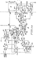
- a presently preferred embodiment 10 of a multiplexing means is connected to a control circuit means 11 for controlling the time intervals of conduction and non-conduction of at least one power switching means 12, connected in series with a load 14, having a load resistance R L" between the first and second line terminals L1 and L2 of an AC source means 16.
- power-switching means 12 comprises a pair of power-switching devices 12a-1 and 12a-2, with each switching device having its controlled-conduction-circuit paralleled by a reverse-conduction element, such as a diode and the like; the series-connected power switching devices 12a have the common junction therebetween connected to a circuit common potential connection 12-1.
- the power switching devices act to substantially connect/disconnect the switching circuit node 12-2a to/from switching circuit node 12-2b, responsive to the state of the signal at a switching control input 12-3.
- the control circuit means 11 receives an on/off control signal (from a load parameter setting/monitoring means (not shown) included in the same integrated circuit having means 10 and 11 therein) at a first input terminal 11-1, and also responsive to various multiplexing means 10 inputs and outputs at terminals 11-2, provides the switching device control signal at an output terminal 11-3.
- the non-shown load setting circuit portion can be of open-loop or closed-loop type and will typically require that an input be provided at a separate terminal to the integrated multiplex/control circuit.
- the power switching devices are advantageously packaged in a module 12 which also includes a pair of switching device voltage sampling resistance elements 12b-1 and 12b-2, each having a resistance R and each connected between one of nodes 12-2a or 12-2b and an associated one of module outputs 12-4a or 12-4b.
- the switching device module 12 advantageously also contains a power supply filter capacitor 12c connected between common potential terminal 12-1 and a terminal 12-5 ( Figure la) at which the control circuit positive operating potential +V is provided.
- switching means 12a-1 and 12a-2 each comprise an insulated-gate transistor 12a-la or 12a-2a, each having: its gate terminal connected in parallel with the gate terminal of the other device and to module control input 12-3; its emitter electrode connected in parallel to circuit common potential terminal 12-1; and its collector electrode connected to one of switching module nodes 12-2a or 12-2b.
- An associated reverse-conduction diode 12a-lb or 12a-2b is formed across the controlled-conduction anode-cathode circuit of each switching device, e.g. across the emitter- collector circuit of each IGT.
- Multiplexing means 10 for providing a plurality of signals (required by control means 11) from information available at the terminals 12-4a and 12-4b of substantially- resistive elements, includes a first comparator means 20, having a non-inverting, + input 20a connected to a multiplexing means first input terminal 10-4a, itself connected to power module first sampling output terminal 12-4a, and an inverting, - input 12b connected to a multiplexing means second input terminal 10-4b, itself connected to power module second sampling output terminal 12-4b.
- First and second switch means 22 and 24 are each of single-pole, double-throw type, having first selectable contact terminals 22a or 24a respectively connected to multiplexing means sample input terminals lO-4b or 10-4a, respectively.
- the second selectable terminals 22b or 24b of these first two switch means are respectively cross-connected to multiplexing means sample input terminal 10-4a or 10-4b, respectively.
- the common terminal 22c of first switch means 22 is connected to circuit common potential, while the common terminal 24b of the second switch means 24 is connected to a first input 26a of a second comparator means 26.
- the switch-position-control inputs 22d and 24d of the first and second switch means 22 and 24 are connected together in parallel to the output 20c of first comparator means 20; first and second switch means 22 and 24 are thus effectively configured as a double-pole, double-throw switch means for alternatingly connecting each of multiplexing means sample input terminals 10-4a or 10-4b either to second comparator input 26a or to common potential, responsive to the logic level at the first comparator means output 20c.
- Another switching means 28 has a first selectable terminal 28a connected to an essentially open circuit, a second selectable terminal 28b connected through another resistance element 30, of resistance magnitude R', to circuit common potential, and a common contact 28c connected to second comparator inverting input 26a.
- the common terminal 28c is controlled between open-circuit terminal 28a and shunt resistance terminal 28b responsive to the logic A signal at a switch means control input 28d.
- switch means 28 is controlled between an essentially open-circuit condition and an essentially short-circuit condition (connecting terminals 28b and 28c)
- I have advantageously utilized a controlled-conduction device 28' having a controlled-conduction circuit between terminals 28'd (connected to circuit common potential) and terminal 28'c (connected to series resistor 30 and thence to comparator input 26a) and having a control input 28'd at which the logic A signal is applied.
- the non-inverting, + input 26b of second comparator 26 receives a selected one of a pair of reference voltages V rl and V r2 .
- Reference voltage V rl (provided by means not shown but well known to the art) is a first positive-polarity voltage, provided at a first selectable terminal 32a of switch means 32.
- the first reference voltage V r1 substantially sets the line-line potential at which the switching device(s) 12a begin to conduct, and is advantageously of small magnitude, e.g. typically between zero volts and the minimum expected forward-conduction voltage drop of devices 12a.
- the second reference voltage V r2 is another positive-polarity voltage, provided at a magnitude greater than the magnitude of first reference voltage V rl , at second switch means selectable terminal 32b.
- the second reference voltage substantially sets the desired level of power-switching device "saturation" voltage, for determination of whether the conducting switching device is in the desired voltage saturation mode or in the undesired active-linear mode; a typical V r2 magnitude is about 3 volts for IGT switching devices 12a-la and 12a-2a.
- the selected one of the two reference voltage is provided at the switch means common terminal 32c, responsive to the state of a reference-voltage-switch logic B signal, provided to switch means control input 32d.
- the single-pole, double-throw switch means comprises first and second controlled-conduction elements 34 and 36, each having one terminal of the controlled-conduction-circuit thereof connected together to the switch means common terminal 32c, and having the remaining controlled-conduction-circuit terminal connected to one of switch means first selectable terminal 32a (device 34) or second selectable terminal 32b (device 36).
- the conduction control input 34a (of that device 34 connected between common terminal 32c and first selectable terminal 32a) is directly connected to the switch means control input 32d, while the remaining controlled-conduction device control input 36a is connected to the output of a logic inverter means 37, having its input connected to switch means control input 32d.
- a first logic level e.g. a high logic level
- one of controlled-conduction devices 34 or 36 e.g. device 34, receives an enabling signal level at its control input, e.g. a high logic level at input 34a, and will conduct to connect one of the selectable terminals, e.g.
- first selectable terminal 32a to the common terminal 32c
- the other device e.g. device 36
- the device e.g. device 36
- formerly in the non-conductive state is switched to the conductive state, connecting second selectable input 32b to common terminal 32c
- the other device e.g. device 34
- the same switch means comprised of an inverter and a pair of controlled-conduction devices, can be utilized for each of switch means 22 and 24.
- the gate control circuit means 11 (enclosed by a chain line) is preferably also part of the same integrated circuit containing the multiplexing means 10.
- multiplexing means 10 also comprises means 38 for providing, in conjunction with the external filter capacitor 12c, a DC voltage of desired polarity (e.g. positive-polarity) from the AC line-line voltage.
- Means 38 advantageously comprises a pair of unidirectionally-conducting devices, such as diodes 38a and 38b, each having an anode connected to one of terminals 10-4a or 10-4b, respectively, and having the cathodes thereof tied together to filter capacitor terminal 10-5 of the integrated circuit, at which terminal the positive operating voltage +V is supplied. It should be understood that means, such as a zener diode 38c or other circuitry well known to the art, can be utilized for regulating operating potential +V, if required.
- Control circuit means 11 includes a two-input AND gate 40, having a first input 40a connected to the on/off control terminal 11-1 of the control circuit means (for connection to the output of an open-loop or a closed-loop control means, not shown, for toggling input 11-1 between a low logic "off” level, e.g. about 0 volts, and a high logic “on” level, e.g. about +V volts).
- the second gate input 40b is connected to another control circuit means input 11-2b, itself connected to the second comparator output 10-2b of the multiplexing means, at which the voltage VZ,L appears.
- the gate output 40c is connected to a first, or turn- on/turn-off control input 44a of a gate drive and dV/dt control means 44, which may be as disclosed in the above- designated application Serial No. 499,579.
- This means has a second, or dV/dt feedback information, input 42b, connected to input 11-2a to receive the V signal at the multiplexing means output 10-2a.
- Means output 44c is connected to control circuit means output 11-3 to supply the IGT gate voltage V g to integrated circuit terminal 10-3 and thence to the control input terminal 12-3 of the switching device module 12, responsive to the signals at inputs 42a and 42b.
- Output 42c is also connected to an inverting, - input 50a of a third comparator means 50, which also has a non-inverting, + input 50b receiving a substantially-constant reference voltage V (substantially equal to the conduction threshold voltage V th above which one of IGTs 12a-la and 12a-2a will be in the conductive condition).
- the third comparator output 50c is connected to the remaining input 44b of the NOR gate, and also provides the logic B signal at control circuit means output 11-2d, for introduction to multiplexing means input 10-2d and thence to the control input 32d of switch means 32.
- the NOR gate output 44c provides the logic A signal to control circuit means output 11-2c, for coupling to multiplexing means input 10-2c and thence to the control electrode 28'd of controlled-conduction means 28'.
- the presently preferred multiplexing means 10 operates, in conjunction with control circuit means 11 and switching device module 12, in the following manner: prior to the initial time t 0 , enough line voltage cycles have occurred to cause rectifiers 38 to conduct to charge filter capacitor 12c to a maximum voltage +V set by the zener voltage of regulator diode 38c, e.g. about +15 volts, to provide operating potential +V.
- the switching devices 12a e.g. IGTs 12a-la and 12a-2a, are in the "off" condition.
- the first comparator output 20c switches to a high logic level, as the potential at the inverting input 20b thereof is no longer more positive than the potential at the non-inverting input 20a.
- switch means 22 and 24 are both operated to connect the respective common terminals 22c and 24c to the respective first selectable terminals 22a and 24a (as shown).
- the line L2 terminal potential appears across resistance 12b-2, as terminals 10-4b and 12-4b are now coupled to common potential by action of switch means 22; this voltage is limited to the conduction voltage drop across now-conducting diode 12a-2b.
- voltage V x is less than the voltage at second comparator input 26b, as the latter voltage is substantially equal to one of reference voltages V r1 or V r2 , both of which reference voltages are of positive polarity.
- the second comparator output 26c voltage therefore switches from a low logic level to a high logic level at zero-crossing time to; if the on/off control input 11-1 is at a high logic level, indicative of the load being commanded to the "on" condition, both AND gate inputs 40a and 40b are at a high logic level, such that the gate output 40c is also at a high logic level, at each line-line potential zero-crossing time t 0 , t0', t 0 ",...etc. Responsive to the high logic level at gate output 40c and input 42a, and to the low level at input 42b, 6utput 42c is switched to a relatively high potential level (approximately equal to the operating potential + V supplied thereto).
- the switching module control voltage V g is at a positive high logic level, switching into conduction that one of the power module devices 12a-la or 12a-2a having a positive anode (collector/drain) voltage thereon, i.e. device 12a-la.
- the high logic level at output 42c appears at third comparator input 50a and is greater than the reference voltage V r (set substantially equal to the switching device conduction threshold voltage V th ) at third comparator second input 50b, causing the third comparator output 50c to be at a low logic level; this low logic level appears as the logic B voltage applied to third switch means control input 32d, causing controlled-conduction device 36 to conduct and apply the second reference voltage V r2 to the second comparator non-inverting input 26b (while the other controlled-conduction device 34 receives a low logic level at its control electrode 34a and is in the substantially non-conductive condition).
- the third comparator output 50c low logic level is also provided to the second input 44b of NOR gate 44, which also receives the high logic level from the AND gate output 40c at its other input 44a; responsive thereto, the NOR gate output 44c provides a low logic level for the logic A signal at the control input 28'd of controlled-conduction device 28'.
- Controlled-conduction device 28' is therefore in the non-conductive condition, and resistance element 30 is not connected between input 26a and circuit common potential.
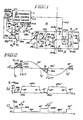
- the voltage V at the output of the precision full-wave rectifier begins to increase in the positive-polarity direction as an initial portion 64a of a sinusoid ( Figure 2b).
- switch means 32 operates to provide the second comparator input 26b with the higher magnitude reference voltage V r2 from switch means 32, as shown by portion 66 of the waveform of Figure 2c.
- the gate signal V g remains at a high logic level and continues to keep the conducting switching device 12a in the conductive condition, if the voltage at input 11-1 remains in the high logic level "on" condition.
- the output 26c of second comparator 26 switches to the high logic level, to provide a low logic level at gate output 40c and input 42a and cause commencement of a controlled-turn-off sequence, thus protecting the switching device. Even if the conducting IGT anode voltage does not exceed the second reference voltage V r2' then when input 11-1 falls to the low logic level "off" control condition at some time t l , gate output 40c provides a low logic level at input 42a which causes commencement of the controlled-turn-off sequence.
- controlled-conduction device 28' conducts and connects to common potential that terminal of resistance element 30 furthest from the V signal node; a voltage-divider (comprised of that one of sampling resistors 12b-1 or 12b-2 associated with that one of power switching devices 12a-la or 12a-2a presently conducting, and resistance element 30) thus acts on the node voltage, to now provide voltage V x .
- the initial turn-off action is followed by means 42 reducing the V g voltage magnitude responsive to the dV/dt information fed back to input 42b through the sampling resistors 12b-1 and 12b-2, in conjunction with the divider resistance 30, to cause the gradual decrease of output 46c voltage.
- This gradual, controlled turn-off action is as illustrated by broken line portion 62a ( Figure 2a), which falling edge replaces the abrupt turn-off edge 62a' which would occur if controlled-turn-off means 42 were not present.
- a time interval i determined by the maximum dV/dt value previously set for means 42, is required from the initiation of turn-off until the completion thereof, such that, for a normal commanded turn-off commencing at time t 1 (responsive to the control voltage at input 11-1 falling to the low logic "off" level), the conducting one of the switching devices is not completely turned off until time t 1 + ⁇ .
- the switching device gate control voltage V g is substantially equal to the switching device conduction threshold voltage, which is itself substantially equal to the reference voltage V r at third comparator input terminal 50b.
- the second comparator reference voltage V 26b continues at the V r2 level during portion 66a and falls to the reference level V r1 at the beginning of a second portion 66b, while the second comparator input 26a voltage substantially linearly rises, as shown in portion 68, substantially to the operating potential +V level, e.g. about 15 volts, established by the zener voltage of diode 38c.
- the voltage V remains substantially at the zener diode 38c voltage (actually at a voltage equal to the sum of the voltage of zener diode 38c and the conduction voltage of that one of conducting diodes 38, plus any additional voltage drop through second switch means 24), as shown in portion 64b, by action of resistances 12b, until the line-line half-cycle waveform decreases to a lesser voltage, during that portion 70 ( Figure 2b) when the source voltage is approaching the zero crossing preparatory to entering the negative-polarity source waveform half-cycle at time t 0 '.
- voltage V is again substantially at the zero magnitude level; the voltage at the other second comparator input (V 26b ) is again at the V r1 level.
- second and third comparators 26 and 50, gates 40 and,44, and means 42 repeat the actions thereof during the positive-polarity half-cycle, whereby the initial conduction portion 72 (Figure 2a) occurs normally until time t 1 ', along with the V x portion 64 ' ( Figure 2b) and the V 26b portion 66' ( Figure 2c).
- time intervals ⁇ and ⁇ ' may, but need not, be equal, as each time interval duration is responsive to the selected maximum value of dV/dt and the switching device anode voltage present at the initiation of the controlled-turn-off action.
- the reference voltage V r1 is thereafter provided to the non-inverting input of the second comparator, as shown by portion 66b', while the inverting input of the second comparator sees the substantially constant voltage portion 64b', which terminates when the source waveform half-cycle decreases in amplitude to provide the falling portion 70', preparatory to the next positive-going zero crossing at time to".
- the entire source waveform cycle portion is completed, with multiplexing means 10 cooperating with control means 11: to detect the zero crossings, at times t 0 , t 0 ', t 0 "...of the source 16 waveform; to monitor the anode voltage of that one of the power switching devices then in conduction, to provide a turn-off action if the conducting device is removed from saturation; to provide a controlled turn-off action, at either the normal "turn-off" time t 1 or at any time prior thereto, but after the associated zero crossing, wherein the decreasing voltage at the anode of the conducting one of device 12a-la or 12a-2a is effectively limited to a previously set maximum dV/dt value; to provide charge to a power supply capacitance during a relatively large portion of the remainder of each source waveform half-cycle; and to automatically prepare the control and multiplexing means for detection of the next source waveform zero crossing and operation in the next half-cycle of the source waveform.
Landscapes
- Engineering & Computer Science (AREA)
- Power Engineering (AREA)
- Inverter Devices (AREA)
- Control Of Electrical Variables (AREA)
Applications Claiming Priority (2)
| Application Number | Priority Date | Filing Date | Title |
|---|---|---|---|
| US06/667,926 US4617508A (en) | 1984-11-02 | 1984-11-02 | Reverse phase-control apparatus for multiplexing interconnections between power switching and control circuit modules |
| US667926 | 1984-11-02 |
Publications (2)
| Publication Number | Publication Date |
|---|---|
| EP0184659A1 true EP0184659A1 (fr) | 1986-06-18 |
| EP0184659B1 EP0184659B1 (fr) | 1991-01-16 |
Family
ID=24680240
Family Applications (1)
| Application Number | Title | Priority Date | Filing Date |
|---|---|---|---|
| EP85113905A Expired - Lifetime EP0184659B1 (fr) | 1984-11-02 | 1985-10-31 | Appareil de multiplexage pour circuits commandés en phase |
Country Status (6)
| Country | Link |
|---|---|
| US (1) | US4617508A (fr) |
| EP (1) | EP0184659B1 (fr) |
| JP (1) | JPH0772851B2 (fr) |
| KR (1) | KR930011850B1 (fr) |
| CA (1) | CA1263439A (fr) |
| DE (1) | DE3581380D1 (fr) |
Cited By (3)
| Publication number | Priority date | Publication date | Assignee | Title |
|---|---|---|---|---|
| BE1002623A4 (fr) * | 1987-12-12 | 1991-04-16 | Insta Elektro Gmbh & Co Kg | Circuit de commande de luminosite pour lampes a incandescence et portions de circuit de distribution electrique. |
| FR2699342A1 (fr) * | 1992-12-14 | 1994-06-17 | Jaeger Regulation | Variateur de puissance moyenne pour courant alternatif et appareil électrique comportant au moins un tel variateur. |
| EP0623991A1 (fr) * | 1993-05-05 | 1994-11-09 | PLUMER (Société Anonyme) | Dispositif de commande de variation de puissance et/ou de vitesse d'une charge |
Families Citing this family (14)
| Publication number | Priority date | Publication date | Assignee | Title |
|---|---|---|---|---|
| US5225765A (en) * | 1984-08-15 | 1993-07-06 | Michael Callahan | Inductorless controlled transition and other light dimmers |
| US5319301A (en) * | 1984-08-15 | 1994-06-07 | Michael Callahan | Inductorless controlled transition and other light dimmers |
| US5629607A (en) * | 1984-08-15 | 1997-05-13 | Callahan; Michael | Initializing controlled transition light dimmers |
| US4633161A (en) * | 1984-08-15 | 1986-12-30 | Michael Callahan | Improved inductorless phase control dimmer power stage with semiconductor controlled voltage rise time |
| US4823069A (en) * | 1984-08-15 | 1989-04-18 | Michael Callahan | Light dimmer for distributed use employing inductorless controlled transition phase control power stage |
| US5004969A (en) * | 1989-10-16 | 1991-04-02 | Bayview Technology Group, Inc. | Phase control switching circuit without zero crossing detection |
| US5239255A (en) * | 1991-02-20 | 1993-08-24 | Bayview Technology Group | Phase-controlled power modulation system |
| US5365148A (en) * | 1992-11-19 | 1994-11-15 | Electronics Diversified, Inc. | Sinusoidal inductorless dimmer providing an amplitude attenuated output |
| US5550440A (en) * | 1994-11-16 | 1996-08-27 | Electronics Diversified, Inc. | Sinusoidal inductorless dimmer applying variable frequency power signal in response to user command |
| FR2802360B1 (fr) * | 1999-12-14 | 2002-03-01 | Legrand Sa | Procede et dispositif d'alimentation electrique d'une charge par un variateur a au moins un interrupteur commande |
| FR2835979B1 (fr) * | 2002-02-08 | 2004-05-07 | Centre Nat Rech Scient | Convertisseur statique d'energie electrique destine a moduler l'energie electrique echangee entre au moins une source de tension et une source de courant |
| FI114588B (fi) * | 2002-12-31 | 2004-11-15 | Lexel Finland Ab Oy | Tehonsäädin |
| US7893680B2 (en) * | 2004-10-27 | 2011-02-22 | Xerox Corporation | Power control using at least 540 degrees of phase |
| US10216523B2 (en) | 2015-07-17 | 2019-02-26 | General Electric Company | Systems and methods for implementing control logic |
Citations (2)
| Publication number | Priority date | Publication date | Assignee | Title |
|---|---|---|---|---|
| US4327309A (en) * | 1980-06-23 | 1982-04-27 | General Electric Company | Fluorescent lamp power supply with low voltage lamp polarity reversal |
| US4484190A (en) * | 1981-05-26 | 1984-11-20 | General Electric Company | System for load output level control |
Family Cites Families (6)
| Publication number | Priority date | Publication date | Assignee | Title |
|---|---|---|---|---|
| US4158150A (en) * | 1978-01-10 | 1979-06-12 | Amf Incorporated | Solid state relay with zero crossover feature |
| US4245184A (en) * | 1979-03-23 | 1981-01-13 | Westinghouse Electric Corp. | AC Solid-state circuit breaker |
| US4274045A (en) * | 1979-04-09 | 1981-06-16 | Richard Goldstein | Power supply and control circuit for series connected controller |
| JPH0313770Y2 (fr) * | 1980-03-13 | 1991-03-28 | ||
| GB2125994A (en) * | 1982-08-25 | 1984-03-14 | Page Eng Co Ltd | A c power control system |
| US4461990A (en) * | 1982-10-01 | 1984-07-24 | General Electric Company | Phase control circuit for low voltage load |
-
1984
- 1984-11-02 US US06/667,926 patent/US4617508A/en not_active Expired - Fee Related
-
1985
- 1985-10-25 CA CA000493907A patent/CA1263439A/fr not_active Expired
- 1985-10-31 EP EP85113905A patent/EP0184659B1/fr not_active Expired - Lifetime
- 1985-10-31 DE DE8585113905T patent/DE3581380D1/de not_active Expired - Lifetime
- 1985-11-01 JP JP60246121A patent/JPH0772851B2/ja not_active Expired - Lifetime
- 1985-11-02 KR KR1019850008176A patent/KR930011850B1/ko not_active Expired - Fee Related
Patent Citations (2)
| Publication number | Priority date | Publication date | Assignee | Title |
|---|---|---|---|---|
| US4327309A (en) * | 1980-06-23 | 1982-04-27 | General Electric Company | Fluorescent lamp power supply with low voltage lamp polarity reversal |
| US4484190A (en) * | 1981-05-26 | 1984-11-20 | General Electric Company | System for load output level control |
Cited By (4)
| Publication number | Priority date | Publication date | Assignee | Title |
|---|---|---|---|---|
| BE1002623A4 (fr) * | 1987-12-12 | 1991-04-16 | Insta Elektro Gmbh & Co Kg | Circuit de commande de luminosite pour lampes a incandescence et portions de circuit de distribution electrique. |
| FR2699342A1 (fr) * | 1992-12-14 | 1994-06-17 | Jaeger Regulation | Variateur de puissance moyenne pour courant alternatif et appareil électrique comportant au moins un tel variateur. |
| EP0623991A1 (fr) * | 1993-05-05 | 1994-11-09 | PLUMER (Société Anonyme) | Dispositif de commande de variation de puissance et/ou de vitesse d'une charge |
| FR2706226A1 (fr) * | 1993-05-05 | 1994-12-16 | Plumer Sa | Dispositif de commande de variation de puissance et/ou de vitesse d'une charge, tel que d'un moteur ou autre. |
Also Published As
| Publication number | Publication date |
|---|---|
| CA1263439A (fr) | 1989-11-28 |
| EP0184659B1 (fr) | 1991-01-16 |
| JPS61115111A (ja) | 1986-06-02 |
| JPH0772851B2 (ja) | 1995-08-02 |
| KR930011850B1 (ko) | 1993-12-21 |
| DE3581380D1 (de) | 1991-02-21 |
| US4617508A (en) | 1986-10-14 |
| KR860004506A (ko) | 1986-06-23 |
Similar Documents
| Publication | Publication Date | Title |
|---|---|---|
| US4617508A (en) | Reverse phase-control apparatus for multiplexing interconnections between power switching and control circuit modules | |
| CN101584249B (zh) | 用于防止不对称电流流过空载的磁低压变压器的调光器 | |
| US6191563B1 (en) | Energy saving power control system | |
| US4328459A (en) | Current inrush limiting apparatus | |
| EP0284412B1 (fr) | Source de puissance à adaptation de tension automatique | |
| EP0622889B1 (fr) | Circuit d'alimentation prérégulateur à basse puissance | |
| US3987356A (en) | Controlled capacitive filter for active loads | |
| JPS60101620A (ja) | 逆位相制御電力スイツチング回路と方法 | |
| US4270058A (en) | Power supply and control circuit for series connected controller | |
| US4571551A (en) | Flyback modulated switching power amplifier | |
| US4447764A (en) | Power supply for low-voltage incandescent lamp and like load | |
| US4791350A (en) | Current regulated switching regulator for gating gate turnoff devices | |
| US4620258A (en) | Circuit for self-commutated turn-off of latched devices, such as of the insulated-gate transistor/rectifier type | |
| US4691143A (en) | Circuit status indicating device with improved switch on/off detection capability | |
| US4771373A (en) | DC power supply with electronically controlled power dissipation | |
| KR900015424A (ko) | 스위치 모드 전원회로 | |
| US4412279A (en) | Switching regulator with transient reduction circuit | |
| US4705963A (en) | AC controlled diode switch | |
| SU1594503A1 (ru) | Устройство дл регулировани температуры | |
| JPH0327408A (ja) | デユーテイ制御装置 | |
| WO2004059825A1 (fr) | Regulateur de courant | |
| RU2046543C1 (ru) | Электронный коммутатор сети переменного тока | |
| SU1246277A1 (ru) | Преобразователь переменного напр жени | |
| SU1642454A1 (ru) | Стабилизирующий преобразователь с импульсным регулированием и с защитой по току | |
| EP0120103A1 (fr) | Circuit pour l'empêchement de la conduction simultanée de deux ou plusieurs commutateurs à courant alternatif |
Legal Events
| Date | Code | Title | Description |
|---|---|---|---|
| PUAI | Public reference made under article 153(3) epc to a published international application that has entered the european phase |
Free format text: ORIGINAL CODE: 0009012 |
|
| AK | Designated contracting states |
Kind code of ref document: A1 Designated state(s): DE FR GB IT SE |
|
| 17P | Request for examination filed |
Effective date: 19861210 |
|
| 17Q | First examination report despatched |
Effective date: 19880808 |
|
| GRAA | (expected) grant |
Free format text: ORIGINAL CODE: 0009210 |
|
| AK | Designated contracting states |
Kind code of ref document: B1 Designated state(s): DE FR GB IT SE |
|
| REF | Corresponds to: |
Ref document number: 3581380 Country of ref document: DE Date of ref document: 19910221 |
|
| ET | Fr: translation filed | ||
| ITF | It: translation for a ep patent filed | ||
| PLBE | No opposition filed within time limit |
Free format text: ORIGINAL CODE: 0009261 |
|
| STAA | Information on the status of an ep patent application or granted ep patent |
Free format text: STATUS: NO OPPOSITION FILED WITHIN TIME LIMIT |
|
| 26N | No opposition filed | ||
| EAL | Se: european patent in force in sweden |
Ref document number: 85113905.5 |
|
| PGFP | Annual fee paid to national office [announced via postgrant information from national office to epo] |
Ref country code: SE Payment date: 19950913 Year of fee payment: 11 Ref country code: FR Payment date: 19950913 Year of fee payment: 11 |
|
| PGFP | Annual fee paid to national office [announced via postgrant information from national office to epo] |
Ref country code: DE Payment date: 19950925 Year of fee payment: 11 |
|
| PGFP | Annual fee paid to national office [announced via postgrant information from national office to epo] |
Ref country code: GB Payment date: 19950927 Year of fee payment: 11 |
|
| PG25 | Lapsed in a contracting state [announced via postgrant information from national office to epo] |
Ref country code: GB Effective date: 19961031 |
|
| PG25 | Lapsed in a contracting state [announced via postgrant information from national office to epo] |
Ref country code: SE Effective date: 19961101 |
|
| GBPC | Gb: european patent ceased through non-payment of renewal fee |
Effective date: 19961031 |
|
| PG25 | Lapsed in a contracting state [announced via postgrant information from national office to epo] |
Ref country code: FR Effective date: 19970630 |
|
| PG25 | Lapsed in a contracting state [announced via postgrant information from national office to epo] |
Ref country code: DE Effective date: 19970701 |
|
| EUG | Se: european patent has lapsed |
Ref document number: 85113905.5 |
|
| REG | Reference to a national code |
Ref country code: FR Ref legal event code: ST |