EP0184917A1 - Plasmareaktorgefäss und Verfahren - Google Patents
Plasmareaktorgefäss und Verfahren Download PDFInfo
- Publication number
- EP0184917A1 EP0184917A1 EP85308526A EP85308526A EP0184917A1 EP 0184917 A1 EP0184917 A1 EP 0184917A1 EP 85308526 A EP85308526 A EP 85308526A EP 85308526 A EP85308526 A EP 85308526A EP 0184917 A1 EP0184917 A1 EP 0184917A1
- Authority
- EP
- European Patent Office
- Prior art keywords
- plasma
- reactor vessel
- confined
- plasma discharge
- substrate
- Prior art date
- Legal status (The legal status is an assumption and is not a legal conclusion. Google has not performed a legal analysis and makes no representation as to the accuracy of the status listed.)
- Granted
Links
- 238000000034 method Methods 0.000 title claims abstract description 20
- 239000000758 substrate Substances 0.000 claims abstract description 24
- 238000004381 surface treatment Methods 0.000 claims abstract description 4
- 230000008021 deposition Effects 0.000 claims description 5
- 239000000463 material Substances 0.000 claims description 3
- 239000004065 semiconductor Substances 0.000 claims 1
- 210000002381 plasma Anatomy 0.000 description 28
- 239000007789 gas Substances 0.000 description 5
- XUIMIQQOPSSXEZ-UHFFFAOYSA-N Silicon Chemical compound [Si] XUIMIQQOPSSXEZ-UHFFFAOYSA-N 0.000 description 4
- 238000005530 etching Methods 0.000 description 4
- 229910052710 silicon Inorganic materials 0.000 description 4
- 239000010703 silicon Substances 0.000 description 4
- 235000012431 wafers Nutrition 0.000 description 4
- BLRPTPMANUNPDV-UHFFFAOYSA-N Silane Chemical compound [SiH4] BLRPTPMANUNPDV-UHFFFAOYSA-N 0.000 description 3
- 229910000077 silane Inorganic materials 0.000 description 3
- IJGRMHOSHXDMSA-UHFFFAOYSA-N Atomic nitrogen Chemical compound N#N IJGRMHOSHXDMSA-UHFFFAOYSA-N 0.000 description 2
- CURLTUGMZLYLDI-UHFFFAOYSA-N Carbon dioxide Chemical compound O=C=O CURLTUGMZLYLDI-UHFFFAOYSA-N 0.000 description 2
- 229910052581 Si3N4 Inorganic materials 0.000 description 2
- VYPSYNLAJGMNEJ-UHFFFAOYSA-N Silicium dioxide Chemical compound O=[Si]=O VYPSYNLAJGMNEJ-UHFFFAOYSA-N 0.000 description 2
- 230000015572 biosynthetic process Effects 0.000 description 2
- 239000011248 coating agent Substances 0.000 description 2
- 238000000576 coating method Methods 0.000 description 2
- 239000004020 conductor Substances 0.000 description 2
- 230000008878 coupling Effects 0.000 description 2
- 238000010168 coupling process Methods 0.000 description 2
- 238000005859 coupling reaction Methods 0.000 description 2
- 238000004090 dissolution Methods 0.000 description 2
- 230000000694 effects Effects 0.000 description 2
- HQVNEWCFYHHQES-UHFFFAOYSA-N silicon nitride Chemical compound N12[Si]34N5[Si]62N3[Si]51N64 HQVNEWCFYHHQES-UHFFFAOYSA-N 0.000 description 2
- 229910052814 silicon oxide Inorganic materials 0.000 description 2
- 229910002092 carbon dioxide Inorganic materials 0.000 description 1
- 239000001569 carbon dioxide Substances 0.000 description 1
- 238000006243 chemical reaction Methods 0.000 description 1
- 238000004132 cross linking Methods 0.000 description 1
- 238000010586 diagram Methods 0.000 description 1
- 239000002657 fibrous material Substances 0.000 description 1
- 239000011491 glass wool Substances 0.000 description 1
- 230000002401 inhibitory effect Effects 0.000 description 1
- 239000000203 mixture Substances 0.000 description 1
- 229910052757 nitrogen Inorganic materials 0.000 description 1
- 230000003287 optical effect Effects 0.000 description 1
- 238000009832 plasma treatment Methods 0.000 description 1
- 238000005086 pumping Methods 0.000 description 1
- 230000005855 radiation Effects 0.000 description 1
- 238000007788 roughening Methods 0.000 description 1
- 239000000126 substance Substances 0.000 description 1
Images
Classifications
-
- H—ELECTRICITY
- H01—ELECTRIC ELEMENTS
- H01J—ELECTRIC DISCHARGE TUBES OR DISCHARGE LAMPS
- H01J37/00—Discharge tubes with provision for introducing objects or material to be exposed to the discharge, e.g. for the purpose of examination or processing thereof
- H01J37/32—Gas-filled discharge tubes
- H01J37/32431—Constructional details of the reactor
- H01J37/32458—Vessel
-
- C—CHEMISTRY; METALLURGY
- C23—COATING METALLIC MATERIAL; COATING MATERIAL WITH METALLIC MATERIAL; CHEMICAL SURFACE TREATMENT; DIFFUSION TREATMENT OF METALLIC MATERIAL; COATING BY VACUUM EVAPORATION, BY SPUTTERING, BY ION IMPLANTATION OR BY CHEMICAL VAPOUR DEPOSITION, IN GENERAL; INHIBITING CORROSION OF METALLIC MATERIAL OR INCRUSTATION IN GENERAL
- C23C—COATING METALLIC MATERIAL; COATING MATERIAL WITH METALLIC MATERIAL; SURFACE TREATMENT OF METALLIC MATERIAL BY DIFFUSION INTO THE SURFACE, BY CHEMICAL CONVERSION OR SUBSTITUTION; COATING BY VACUUM EVAPORATION, BY SPUTTERING, BY ION IMPLANTATION OR BY CHEMICAL VAPOUR DEPOSITION, IN GENERAL
- C23C16/00—Chemical coating by decomposition of gaseous compounds, without leaving reaction products of surface material in the coating, i.e. chemical vapour deposition [CVD] processes
- C23C16/44—Chemical coating by decomposition of gaseous compounds, without leaving reaction products of surface material in the coating, i.e. chemical vapour deposition [CVD] processes characterised by the method of coating
- C23C16/50—Chemical coating by decomposition of gaseous compounds, without leaving reaction products of surface material in the coating, i.e. chemical vapour deposition [CVD] processes characterised by the method of coating using electric discharges
- C23C16/515—Chemical coating by decomposition of gaseous compounds, without leaving reaction products of surface material in the coating, i.e. chemical vapour deposition [CVD] processes characterised by the method of coating using electric discharges using pulsed discharges
-
- H—ELECTRICITY
- H01—ELECTRIC ELEMENTS
- H01J—ELECTRIC DISCHARGE TUBES OR DISCHARGE LAMPS
- H01J37/00—Discharge tubes with provision for introducing objects or material to be exposed to the discharge, e.g. for the purpose of examination or processing thereof
- H01J37/32—Gas-filled discharge tubes
- H01J37/32009—Arrangements for generation of plasma specially adapted for examination or treatment of objects, e.g. plasma sources
- H01J37/32082—Radio frequency generated discharge
- H01J37/321—Radio frequency generated discharge the radio frequency energy being inductively coupled to the plasma
-
- H—ELECTRICITY
- H01—ELECTRIC ELEMENTS
- H01J—ELECTRIC DISCHARGE TUBES OR DISCHARGE LAMPS
- H01J37/00—Discharge tubes with provision for introducing objects or material to be exposed to the discharge, e.g. for the purpose of examination or processing thereof
- H01J37/32—Gas-filled discharge tubes
- H01J37/32431—Constructional details of the reactor
- H01J37/32623—Mechanical discharge control means
Definitions
- This invention relates to pulsed radio frequency plasma treatment of substrate bodies and in particular to a reactor vessel for use in said treatment.
- Plasma processing and in particular low temperature glow discharge plasma processing is potentially a very useful process for the surface processing of substrate materials.
- the pulsed plasma discharge is of high intensity but of low average power. During each 'on' period an intense radio frequency grade causes substantially complete dissolution of the gas constituting the plasma. The active species thus produced during the pulse then react in the subsequent 'off' period.
- a method of surface treatment of a substrate body by exposing the body surface to a pulsed radio frequency plasma discharge, the plasma being substantially completely dissociated during each said pulse, characterised in that the plasma discharge is confined to a region adjacent the body surface.
- a reactor vessel for treatment of a laminar substrate body surface with a pulsed radio-frequency plasma characterised in that the reactor has a substantially rectangular cross section corresponding to the configuration of the body whereby, in use, the plasma is confined adjacent the body surface.
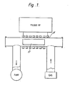
- the plasma reactor vessel comprises a tubular body 11 having a cross-sectioned configuration corresponding to the shape of a substrate body 12 to be processed.
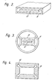
- the reactor vessel 11 is rectangular in cross-section as is shown in Fig. 2.
- the plasma may be restricted to a region adjacent the substrate by shaped insert 13 (Fig. 3) placed in the vessel 11 and surrounding the body 12.
- a low pressure gas from which the plasma is to be formed is pumped through the vessel 11.
- the plasma is maintained at a pressure of 1 to 1000 mtorr.
- the space between the insert 13 and the vessel 11 is sealed and pumped separately to a pressure high enough, typically 100 to 200 torr, to inhibit plasma formation.
- a pressure high enough typically 100 to 200 torr
- the same effect may be achieved by filling this space with a fibrous material, e.g. glass wool.
- pulsed radio frequency power is applied to the reactor vessel 11 via a work coil 13 surrounding the vessel and coupled to a generator (not shown).
- the power output of the generator is not critical but must be sufficient to provide the desired surface processing effect, i.e. sufficient to provide substantially complete dissolution of the plasma.
- pulse powers of 200 w/cm 2 to 250 w/cm 2 of the treated surface are adequate for this purpose.
- the etching or deposition rate may be improved by the provision of longitudinal grooves 14 (Fig. 4) in the wall of the vessel 11 or the insert 13.
- the provision of longitudinal grooves in the insert 13 or the vessel 11 inhibits the formation of a continuous conductor loop which would provide a 'shorted turn' inhibiting coupling of radio frequency power to the plasma.
- the grooves should have a small opening and a relatively large internal surface area.
- the generator pulse rate is matched to the gas exchange rate within the reactor vessel, i.e. the pulse rate is matched to the pumping speed such that one pulse is applied for each replenishment of gas in the vessel 11.
- the pulse rate is matched to the pumping speed such that one pulse is applied for each replenishment of gas in the vessel 11.
- the pulsed plasma should be confined to a region within 15 to 25 mm from the substrate surface. If, for example, the substrate is a circuit board 1 to 4 mm in thickness then the smaller dimension of the rectangular cross-section of the vessel 11 should be 31 to 44 mm.
- silicon wafer substrates with silicon nitride, silicon oxide and silicon using both confined and unconfined plasmas.
- Films of silicon nitride (from silane and nitrogen), silicon oxide (from silane and carbon dioxide) and silicon (from silane) have been deposited on 4 inch silicon wafers.
- Examination of interference fringes using light of a wavelength of 5000 A has shown that, for plasma confinement to the range specified above, a uniformity of 2500 A over the wafer surface of the above surface films is achieved for coating thicknesses in the range 0.3 to 5 microns. Outside this confinement region surface variations greater than 2,500 A were observed.
- Deposition was performed at pressures in the range 1 to 1000 mtorr and a greater pulse power density of 220 watt/cm 2 of the wafer surface.
Landscapes
- Chemical & Material Sciences (AREA)
- Engineering & Computer Science (AREA)
- Physics & Mathematics (AREA)
- Plasma & Fusion (AREA)
- Analytical Chemistry (AREA)
- Mechanical Engineering (AREA)
- Chemical Kinetics & Catalysis (AREA)
- Materials Engineering (AREA)
- General Chemical & Material Sciences (AREA)
- Metallurgy (AREA)
- Organic Chemistry (AREA)
- ing And Chemical Polishing (AREA)
- Chemical Vapour Deposition (AREA)
- Drying Of Semiconductors (AREA)
- Plasma Technology (AREA)
- Transition And Organic Metals Composition Catalysts For Addition Polymerization (AREA)
- Physical Or Chemical Processes And Apparatus (AREA)
- Crystals, And After-Treatments Of Crystals (AREA)
- Investigating, Analyzing Materials By Fluorescence Or Luminescence (AREA)
Priority Applications (1)
| Application Number | Priority Date | Filing Date | Title |
|---|---|---|---|
| AT85308526T ATE54340T1 (de) | 1984-12-13 | 1985-11-25 | Plasmareaktorgefaess und verfahren. |
Applications Claiming Priority (2)
| Application Number | Priority Date | Filing Date | Title |
|---|---|---|---|
| GB8431422 | 1984-12-13 | ||
| GB848431422A GB8431422D0 (en) | 1984-12-13 | 1984-12-13 | Plasma reactor vessel |
Publications (2)
| Publication Number | Publication Date |
|---|---|
| EP0184917A1 true EP0184917A1 (de) | 1986-06-18 |
| EP0184917B1 EP0184917B1 (de) | 1990-07-04 |
Family
ID=10571102
Family Applications (1)
| Application Number | Title | Priority Date | Filing Date |
|---|---|---|---|
| EP85308526A Expired - Lifetime EP0184917B1 (de) | 1984-12-13 | 1985-11-25 | Plasmareaktorgefäss und Verfahren |
Country Status (5)
| Country | Link |
|---|---|
| EP (1) | EP0184917B1 (de) |
| JP (1) | JPH0689462B2 (de) |
| AT (1) | ATE54340T1 (de) |
| DE (1) | DE3578562D1 (de) |
| GB (2) | GB8431422D0 (de) |
Cited By (3)
| Publication number | Priority date | Publication date | Assignee | Title |
|---|---|---|---|---|
| EP0207767A3 (en) * | 1985-06-29 | 1989-02-08 | Stc Plc | Pulsed plasma apparatus and process |
| GB2244285A (en) * | 1990-05-03 | 1991-11-27 | Northern Telecom Ltd | Phosphide films produced by pulsed plasma deposition |
| US12311759B1 (en) | 2022-02-02 | 2025-05-27 | Consumer Safety Technology, Llc | Wireless vehicle interface for immobilization system |
Families Citing this family (3)
| Publication number | Priority date | Publication date | Assignee | Title |
|---|---|---|---|---|
| GB8905075D0 (en) * | 1989-03-06 | 1989-04-19 | Nordiko Ltd | Electrode assembly and apparatus |
| US6129808A (en) * | 1998-03-31 | 2000-10-10 | Lam Research Corporation | Low contamination high density plasma etch chambers and methods for making the same |
| DE19923018C2 (de) * | 1999-05-19 | 2001-09-27 | Univ Dresden Tech | Vorrichtung zur Bearbeitung bandförmiger Werkstücke mit Hilfe resonanter Hochfrequenzplasmen |
Citations (12)
| Publication number | Priority date | Publication date | Assignee | Title |
|---|---|---|---|---|
| DE2340442A1 (de) * | 1973-08-03 | 1975-02-20 | Mitsubishi Electric Corp | Verfahren zur herstellung von halbleiterelementen |
| DE2848691A1 (de) * | 1977-11-11 | 1979-05-17 | Dionex Corp | Verfahren und gas zur behandlung von halbleiter-bauelementen |
| DE2810554B2 (de) * | 1977-03-11 | 1980-01-03 | Fujitsu Ltd., Kawasaki, Kanagawa (Japan) | Vorrichtung zur Plasmabehandlung bei der Halbleiterbauelementeherstellung |
| EP0027578A1 (de) * | 1979-10-17 | 1981-04-29 | Texas Instruments Incorporated | Radiofrequenzplasma-Ätzapparat mit einer Elektrode und Verfahren zum Ätzen unter Verwendung eines solchen Apparats |
| EP0032788A1 (de) * | 1980-01-16 | 1981-07-29 | National Research Development Corporation | Verfahren zum Aufbringen einer Beschichtung mittels Glimmentladung |
| DE3015034A1 (de) * | 1980-04-18 | 1981-10-29 | Fraunhofer-Gesellschaft zur Förderung der angewandten Forschung e.V., 8000 München | Verfahren zur herstellung von mikrostrukturen auf festen koerpern |
| US4333814A (en) * | 1979-12-26 | 1982-06-08 | Western Electric Company, Inc. | Methods and apparatus for improving an RF excited reactive gas plasma |
| DE3103177A1 (de) * | 1981-01-30 | 1982-08-26 | Siemens AG, 1000 Berlin und 8000 München | Verfahren zum herstellen von polysiliziumstrukturen bis in den 1 (my)m-bereich auf integrierte halbleiterschaltungen enthaltenden substraten durch plasmaaetzen |
| US4358686A (en) * | 1980-01-25 | 1982-11-09 | Mitsubishi Denki Kabushiki Kaisha | Plasma reaction device |
| DE3214626A1 (de) * | 1981-04-20 | 1982-11-25 | LFE Corp., 01510 Clinton, Mass. | Verfahren zum selektiven aetzen von polykristallinem siliziummaterial |
| GB2105729A (en) * | 1981-09-15 | 1983-03-30 | Itt Ind Ltd | Surface processing of a substrate material |
| EP0104916A2 (de) * | 1982-09-29 | 1984-04-04 | National Research Development Corporation | Niederschlag eines Films auf einem Substrat durch Elektronenstrahlbedampfung |
Family Cites Families (6)
| Publication number | Priority date | Publication date | Assignee | Title |
|---|---|---|---|---|
| BE526527A (de) * | 1953-02-17 | |||
| BE555721A (de) * | 1956-03-12 | |||
| JPS5738921Y2 (de) * | 1977-12-28 | 1982-08-27 | ||
| EP0095200B1 (de) * | 1982-05-21 | 1989-03-15 | Tegal Corporation | Ausnehmbares Teil eines Plasmareaktors |
| JPS59119729A (ja) * | 1982-12-25 | 1984-07-11 | Fujitsu Ltd | マイクロ波処理方法及び装置 |
| JPS59171491A (ja) * | 1983-03-18 | 1984-09-27 | 富士通株式会社 | マイクロ波処理方法及び処理装置 |
-
1984
- 1984-12-13 GB GB848431422A patent/GB8431422D0/en active Pending
-
1985
- 1985-11-25 GB GB08528999A patent/GB2170350B/en not_active Expired
- 1985-11-25 AT AT85308526T patent/ATE54340T1/de not_active IP Right Cessation
- 1985-11-25 EP EP85308526A patent/EP0184917B1/de not_active Expired - Lifetime
- 1985-11-25 DE DE8585308526T patent/DE3578562D1/de not_active Revoked
- 1985-12-11 JP JP60278838A patent/JPH0689462B2/ja not_active Expired - Fee Related
Patent Citations (12)
| Publication number | Priority date | Publication date | Assignee | Title |
|---|---|---|---|---|
| DE2340442A1 (de) * | 1973-08-03 | 1975-02-20 | Mitsubishi Electric Corp | Verfahren zur herstellung von halbleiterelementen |
| DE2810554B2 (de) * | 1977-03-11 | 1980-01-03 | Fujitsu Ltd., Kawasaki, Kanagawa (Japan) | Vorrichtung zur Plasmabehandlung bei der Halbleiterbauelementeherstellung |
| DE2848691A1 (de) * | 1977-11-11 | 1979-05-17 | Dionex Corp | Verfahren und gas zur behandlung von halbleiter-bauelementen |
| EP0027578A1 (de) * | 1979-10-17 | 1981-04-29 | Texas Instruments Incorporated | Radiofrequenzplasma-Ätzapparat mit einer Elektrode und Verfahren zum Ätzen unter Verwendung eines solchen Apparats |
| US4333814A (en) * | 1979-12-26 | 1982-06-08 | Western Electric Company, Inc. | Methods and apparatus for improving an RF excited reactive gas plasma |
| EP0032788A1 (de) * | 1980-01-16 | 1981-07-29 | National Research Development Corporation | Verfahren zum Aufbringen einer Beschichtung mittels Glimmentladung |
| US4358686A (en) * | 1980-01-25 | 1982-11-09 | Mitsubishi Denki Kabushiki Kaisha | Plasma reaction device |
| DE3015034A1 (de) * | 1980-04-18 | 1981-10-29 | Fraunhofer-Gesellschaft zur Förderung der angewandten Forschung e.V., 8000 München | Verfahren zur herstellung von mikrostrukturen auf festen koerpern |
| DE3103177A1 (de) * | 1981-01-30 | 1982-08-26 | Siemens AG, 1000 Berlin und 8000 München | Verfahren zum herstellen von polysiliziumstrukturen bis in den 1 (my)m-bereich auf integrierte halbleiterschaltungen enthaltenden substraten durch plasmaaetzen |
| DE3214626A1 (de) * | 1981-04-20 | 1982-11-25 | LFE Corp., 01510 Clinton, Mass. | Verfahren zum selektiven aetzen von polykristallinem siliziummaterial |
| GB2105729A (en) * | 1981-09-15 | 1983-03-30 | Itt Ind Ltd | Surface processing of a substrate material |
| EP0104916A2 (de) * | 1982-09-29 | 1984-04-04 | National Research Development Corporation | Niederschlag eines Films auf einem Substrat durch Elektronenstrahlbedampfung |
Non-Patent Citations (1)
| Title |
|---|
| PATENT ABSTRACTS OF JAPAN, unexamined applications, C field, vol. 6, no. 227, Noember 12, 1982 THE PATENT OFFICE JAPANESE GOVERNMENT page 144 C 134 * |
Cited By (4)
| Publication number | Priority date | Publication date | Assignee | Title |
|---|---|---|---|---|
| EP0207767A3 (en) * | 1985-06-29 | 1989-02-08 | Stc Plc | Pulsed plasma apparatus and process |
| GB2244285A (en) * | 1990-05-03 | 1991-11-27 | Northern Telecom Ltd | Phosphide films produced by pulsed plasma deposition |
| GB2244285B (en) * | 1990-05-03 | 1994-01-26 | Northern Telecom Ltd | Phosphide films |
| US12311759B1 (en) | 2022-02-02 | 2025-05-27 | Consumer Safety Technology, Llc | Wireless vehicle interface for immobilization system |
Also Published As
| Publication number | Publication date |
|---|---|
| ATE54340T1 (de) | 1990-07-15 |
| JPS61149486A (ja) | 1986-07-08 |
| DE3578562D1 (de) | 1990-08-09 |
| GB8528999D0 (en) | 1986-01-02 |
| GB8431422D0 (en) | 1985-01-23 |
| JPH0689462B2 (ja) | 1994-11-09 |
| GB2170350A (en) | 1986-07-30 |
| GB2170350B (en) | 1988-11-02 |
| EP0184917B1 (de) | 1990-07-04 |
Similar Documents
| Publication | Publication Date | Title |
|---|---|---|
| KR890002732B1 (ko) | 마이크로파 프라즈마 처리방법 및 그 장치 | |
| KR100498584B1 (ko) | 플라즈마처리장치및플라즈마처리방법 | |
| US6823816B2 (en) | Plasma processing system | |
| EP0874386B1 (de) | Vorrichtung und Verfahren zur Remote-Plasma Erzeugung durch Mikrowellen | |
| US4987284A (en) | Downstream microwave plasma processing apparatus having an improved coupling structure between microwave plasma | |
| EP0830052A1 (de) | Vorrichtung und verfahren zur plasmabehandlung | |
| US5011705A (en) | Plasma processing method | |
| JPWO2000074127A1 (ja) | プラズマプロセス装置 | |
| WO2000074127A1 (en) | Plasma process device | |
| KR100220132B1 (ko) | 마이크로파 플라즈마 처리 장치 및 마이크로파 플라즈마 처리 방법 | |
| JP2003109941A (ja) | プラズマ処理装置および表面処理方法 | |
| KR20040021621A (ko) | 플라즈마 공정에서 마이크로-제트 인에이블되는 저 에너지이온 생성 및 이송을 위한 방법과 장치 | |
| US4749589A (en) | Method of surface treatment | |
| KR100509387B1 (ko) | 플라즈마 처리 방법 | |
| EP0184917B1 (de) | Plasmareaktorgefäss und Verfahren | |
| KR100218836B1 (ko) | 플라스마 처리장치 | |
| JPH11145116A (ja) | マイクロ波プラズマ処理装置及びその実施に使用する対向電極 | |
| JPH01184922A (ja) | エッチング、アッシング及び成膜等に有用なプラズマ処理装置 | |
| JP3530788B2 (ja) | マイクロ波供給器及びプラズマ処理装置並びに処理方法 | |
| KR100272143B1 (ko) | 반도체 제조장치 및 그 드라이클리닝 방법 | |
| JPS63100186A (ja) | マイクロ波プラズマ処理装置 | |
| JP3784912B2 (ja) | マイクロ波励起プラズマ装置 | |
| KR100425658B1 (ko) | 마이크로파 공급기, 이를 구비한 플라즈마 처리 장치, 및 플라즈마 처리 방법 | |
| JP2005159049A (ja) | プラズマ成膜方法 | |
| JPH1074730A (ja) | 表面処理装置 |
Legal Events
| Date | Code | Title | Description |
|---|---|---|---|
| PUAI | Public reference made under article 153(3) epc to a published international application that has entered the european phase |
Free format text: ORIGINAL CODE: 0009012 |
|
| AK | Designated contracting states |
Kind code of ref document: A1 Designated state(s): AT BE CH DE FR IT LI LU NL SE |
|
| 17P | Request for examination filed |
Effective date: 19860905 |
|
| RAP1 | Party data changed (applicant data changed or rights of an application transferred) |
Owner name: STC PLC |
|
| 17Q | First examination report despatched |
Effective date: 19881004 |
|
| GRAA | (expected) grant |
Free format text: ORIGINAL CODE: 0009210 |
|
| RAP1 | Party data changed (applicant data changed or rights of an application transferred) |
Owner name: STC PLC |
|
| AK | Designated contracting states |
Kind code of ref document: B1 Designated state(s): AT BE CH DE FR IT LI LU NL SE |
|
| PG25 | Lapsed in a contracting state [announced via postgrant information from national office to epo] |
Ref country code: SE Effective date: 19900704 Ref country code: IT Free format text: LAPSE BECAUSE OF FAILURE TO SUBMIT A TRANSLATION OF THE DESCRIPTION OR TO PAY THE FEE WITHIN THE PRESCRIBED TIME-LIMIT;WARNING: LAPSES OF ITALIAN PATENTS WITH EFFECTIVE DATE BEFORE 2007 MAY HAVE OCCURRED AT ANY TIME BEFORE 2007. THE CORRECT EFFECTIVE DATE MAY BE DIFFERENT FROM THE ONE RECORDED. Effective date: 19900704 Ref country code: BE Effective date: 19900704 Ref country code: AT Effective date: 19900704 |
|
| REF | Corresponds to: |
Ref document number: 54340 Country of ref document: AT Date of ref document: 19900715 Kind code of ref document: T |
|
| ET | Fr: translation filed | ||
| REF | Corresponds to: |
Ref document number: 3578562 Country of ref document: DE Date of ref document: 19900809 |
|
| REG | Reference to a national code |
Ref country code: CH Ref legal event code: PL |
|
| PG25 | Lapsed in a contracting state [announced via postgrant information from national office to epo] |
Ref country code: LU Free format text: LAPSE BECAUSE OF NON-PAYMENT OF DUE FEES Effective date: 19901130 Ref country code: LI Free format text: LAPSE BECAUSE OF NON-PAYMENT OF DUE FEES Effective date: 19901130 Ref country code: CH Free format text: LAPSE BECAUSE OF NON-PAYMENT OF DUE FEES Effective date: 19901130 |
|
| PLBI | Opposition filed |
Free format text: ORIGINAL CODE: 0009260 |
|
| 26 | Opposition filed |
Opponent name: LEYBOLD AKTIENGESELLSCHAFT Effective date: 19910402 |
|
| NLR1 | Nl: opposition has been filed with the epo |
Opponent name: LEYBOLD AG. |
|
| PGFP | Annual fee paid to national office [announced via postgrant information from national office to epo] |
Ref country code: FR Payment date: 19921027 Year of fee payment: 8 |
|
| PGFP | Annual fee paid to national office [announced via postgrant information from national office to epo] |
Ref country code: NL Payment date: 19921130 Year of fee payment: 8 |
|
| PGFP | Annual fee paid to national office [announced via postgrant information from national office to epo] |
Ref country code: DE Payment date: 19930201 Year of fee payment: 8 |
|
| RDAG | Patent revoked |
Free format text: ORIGINAL CODE: 0009271 |
|
| STAA | Information on the status of an ep patent application or granted ep patent |
Free format text: STATUS: PATENT REVOKED |
|
| 27W | Patent revoked |
Effective date: 19930326 |
|
| REG | Reference to a national code |
Ref country code: CH Ref legal event code: PL |
|
| NLR2 | Nl: decision of opposition |