EP0185199B1 - Récepteur optique à réaction négative - Google Patents
Récepteur optique à réaction négative Download PDFInfo
- Publication number
- EP0185199B1 EP0185199B1 EP85114446A EP85114446A EP0185199B1 EP 0185199 B1 EP0185199 B1 EP 0185199B1 EP 85114446 A EP85114446 A EP 85114446A EP 85114446 A EP85114446 A EP 85114446A EP 0185199 B1 EP0185199 B1 EP 0185199B1
- Authority
- EP
- European Patent Office
- Prior art keywords
- optical receiver
- fet
- bipolar transistor
- amplifier
- light receiving
- Prior art date
- Legal status (The legal status is an assumption and is not a legal conclusion. Google has not performed a legal analysis and makes no representation as to the accuracy of the status listed.)
- Expired - Lifetime
Links
- 230000003287 optical effect Effects 0.000 title claims description 29
- 230000005669 field effect Effects 0.000 claims description 22
- 239000003990 capacitor Substances 0.000 claims description 5
- 230000008878 coupling Effects 0.000 claims 1
- 238000010168 coupling process Methods 0.000 claims 1
- 238000005859 coupling reaction Methods 0.000 claims 1
- 230000003071 parasitic effect Effects 0.000 description 12
- 238000010586 diagram Methods 0.000 description 7
- 230000000295 complement effect Effects 0.000 description 4
- 230000000694 effects Effects 0.000 description 4
- 230000000052 comparative effect Effects 0.000 description 3
- 230000003321 amplification Effects 0.000 description 2
- 230000008901 benefit Effects 0.000 description 2
- 238000004891 communication Methods 0.000 description 2
- 230000007423 decrease Effects 0.000 description 2
- 238000012986 modification Methods 0.000 description 2
- 230000004048 modification Effects 0.000 description 2
- 238000003199 nucleic acid amplification method Methods 0.000 description 2
- 238000013459 approach Methods 0.000 description 1
- 238000000034 method Methods 0.000 description 1
- 239000013307 optical fiber Substances 0.000 description 1
- 238000006467 substitution reaction Methods 0.000 description 1
- 238000012360 testing method Methods 0.000 description 1
Images


Classifications
-
- H—ELECTRICITY
- H04—ELECTRIC COMMUNICATION TECHNIQUE
- H04B—TRANSMISSION
- H04B10/00—Transmission systems employing electromagnetic waves other than radio-waves, e.g. infrared, visible or ultraviolet light, or employing corpuscular radiation, e.g. quantum communication
-
- H—ELECTRICITY
- H04—ELECTRIC COMMUNICATION TECHNIQUE
- H04B—TRANSMISSION
- H04B10/00—Transmission systems employing electromagnetic waves other than radio-waves, e.g. infrared, visible or ultraviolet light, or employing corpuscular radiation, e.g. quantum communication
- H04B10/60—Receivers
- H04B10/66—Non-coherent receivers, e.g. using direct detection
- H04B10/69—Electrical arrangements in the receiver
- H04B10/693—Arrangements for optimizing the preamplifier in the receiver
Definitions
- This invention relates generally to an optical receiver with negative feedback for converting optical signals into electrical signals. according to the preamble part of claim 1. Such circuits are used in optical communication systems.
- an optical receiver which comprises a photosensitive detector and means for amplifying the electrical signal output from that detector.
- the amplifying means comprise a plurality of field effect transistors and an inverting amplifier for inversely amplifying the output of said FETs.
- an amplifier includes a photosensitive detector coupled to a pair of cascode field effect transistors arranged to operate at substantial unity gain.
- the total input capacitance of an amplifier or preamplifier of signals from a transducer are neutralized by providing a positive feedback path from one transistor in cascade relation with a second transistor.
- the feedback path includes the input capacitances and thereby neutralizes them to the extent that the gain of the cascade amplifiers approach unity.
- the cathode of a light receiving element 11 is connected to the positive pole of a power supply 12 to apply a reverse bias voltage to the circuit.
- the anode of light receiving element 11 is connected to the input of an inverting amplifier 13.
- Light received by light receiving element 11 is converted into an optical output electrical signal, which is inverted and amplified by inverting amplifier 13.
- the output of amplifier 13 is fed back to the input of the inverting amplifier 13 through a feedback resistor 14.
- a parasitic capacitance 15 and an input capacitance 16 exist in the light receiving element 11 and the inverted amplifier 13, respectively as shown by a short dashes line in Fig. 2.
- an upper cut-off frequency f C1 of the frequency characteristics of the optical receiver is approximated by the following equation.
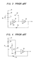
- Fig. 3 shows another conventional optical receiver configuration wherein the same negative feedback type transimpedance method as that of Fig. 2 has been adopted.
- an amplifier 21 providing a gain of 1 is connected between the anode of the light receiving element 11 and the inverted amplifier 13.
- the output voltage of the amplifier 21 is further applied to the cathode of the light receiving element 11 through a capacitor 22.
- a resistor 23 is connected between the cathode of the light receiving element 11 and the power supply 12.
- Light receiving element 11 in that circuit is provided with positive feedback, by a bootstrap feedback arrangement. Since the a.c. voltage on the anode side of the light receiving element is applied to the amplifier 21 with a gain of unity (1) and the output is applied to the cathode of the light receiving element 11 through the capacitor 22, the a.c. potential applied across the light receiving element 11 becomes equal. Consequently, the potential difference between both ends of the parasitic capacitance is always zero. Thus the parasitic capacitance 15 will not affect the frequency characteristics of the optical receiver.
- Fig. 4 shows a circuit configuration employing a field effect transistor 31 corresponding to the amplifier 21 shown in Fig. 3 (PRIOR ART).
- the drain terminal of the field effect transistor 31 is connected to the power supply 12 and one end of the resistor 23; the gate terminal to the anode of the light receiving element 11 and one end of the feedback resistor 14; and the source terminal to one end of a source resistor 32, the input of the inverted amplifier 13 and one end of the capacitor 22.
- the source follower circuit of a field effect transistor has a gain close to 1 and besides the gain will never exceed 1. Moreover, the advantage is that the input capacitance of the source follower circuit can be made smaller than that of an emitter follower circuit using a bipolar transistor and thus a wider frequency band is available.
- the upper cut-off frequenc fc 2 in the negative feedback transimpedance type optical receiver utilizing the bootstrap of Fig. 3 is expressed by Eq. (2) to define the gain of the amplifier at the initial stage as 1 and the output impedance as zero. But that definition is limited to an ideal case.
- This objective is solved by an optical receiver comprising the characterizing features of Claim 1.
- the amplifier comprising the field effect transistor and the bipolar transistor complementary thereto as recited in the characterizing part of Claim 1 has a substantially unity voltage gain further closer to 1 and its output impedance can be minimized. For that reason, the influence of a parasitic capacitance on the light receiving element is reduced and the upper cut-off frequency of the optical receiver according to the present invention becomes higher, whereby the bootstrap effect is obtainable satisfactorily even at high frequencies.
- Preferred embodiments are subject to the Subclaims.
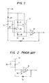
- Fig. 1 shows an embodiment of the present invention wherein like reference characters designate like elements of Fig. 4, the description of which will be omitted.
- the field effect transistor 31 is assumed that of an n-channel type.
- a pnp bipolar transistor 1 complementary to the field effect transistor 31 is directly connected to the field effect transistor 31; i.e., the base of the bipolar transistor 1 is connected to the drain terminal of the field effect transistor 31 and one end of a resistor 2; the emitter of the bipolar transistor 1 to the positive pole of a power supply 12, one end of resistor 23 and the other end of a resistor 2; and the collector of the bipolar transistor 1 to the source terminal of the field effect transistor 31, one end of a source resistor 32, one end of a capacitor 22 and an inverted amplifier 13.
- the field effect transistor 31, the bipolar transistor 1, the source resistor 32 and the resistor 2 constitute an amplifier 3 shown by short dashes lines in Fig. 1.
- the amplifier 3 was composed of the n-channel type field effect transistor 31 and the pnp type bipolar transistor 1 in the aforementioned example, the amplifier 3 may be composed of a p-channel type field effect transistor and an npn bipolar transistor complementary thereto.
- the optical receiver according to the present invention is capable of satisfactorily cancelling parasitic capacitance of the light receiving element by means of the bootstrap effect and functioning in a frequency range of as high as tens of MHz or higher. Accordingly, the circuit is fit for use in large capacity, high-speed data communications using optical fibers.
- Fig. 5(a) is a graph showing comparative frequency response of a conventional photoelectric converting circuit, an FET circuit without and with the added bipolar transistor.
- Fig. 5(b) is a schematic diagram of an FET circuit.
- Fig. 5(c) is a schematic diagram of an FET circuit with an added bipolar transistor.
- Fig. 6 shows comparative test results.
- Fig. 6(c) there is shown a circuit diagram of the present invention using the additional bipolar transistor and a graph of the frequency response of the circuit. As shown in the graph, the response is flat over a wider frequency range than with either of the PRIOR ART configurations.
Landscapes
- Physics & Mathematics (AREA)
- Electromagnetism (AREA)
- Engineering & Computer Science (AREA)
- Computer Networks & Wireless Communication (AREA)
- Signal Processing (AREA)
- Amplifiers (AREA)
- Optical Communication System (AREA)
- Light Receiving Elements (AREA)
Claims (5)
caractérisé en ce qu'il comprend en outre :
Applications Claiming Priority (2)
| Application Number | Priority Date | Filing Date | Title |
|---|---|---|---|
| JP59239095A JPS61117910A (ja) | 1984-11-13 | 1984-11-13 | 光電変換回路 |
| JP239095/84 | 1984-11-13 |
Publications (3)
| Publication Number | Publication Date |
|---|---|
| EP0185199A2 EP0185199A2 (fr) | 1986-06-25 |
| EP0185199A3 EP0185199A3 (en) | 1988-09-21 |
| EP0185199B1 true EP0185199B1 (fr) | 1993-04-21 |
Family
ID=17039735
Family Applications (1)
| Application Number | Title | Priority Date | Filing Date |
|---|---|---|---|
| EP85114446A Expired - Lifetime EP0185199B1 (fr) | 1984-11-13 | 1985-11-13 | Récepteur optique à réaction négative |
Country Status (7)
| Country | Link |
|---|---|
| US (1) | US4638152A (fr) |
| EP (1) | EP0185199B1 (fr) |
| JP (1) | JPS61117910A (fr) |
| KR (1) | KR900006294B1 (fr) |
| AU (1) | AU572362B2 (fr) |
| DE (1) | DE3587285T2 (fr) |
| HK (1) | HK92093A (fr) |
Families Citing this family (10)
| Publication number | Priority date | Publication date | Assignee | Title |
|---|---|---|---|---|
| DE3803034C3 (de) * | 1988-02-02 | 1994-10-20 | Sick Optik Elektronik Erwin | Photoempfänger |
| JPH0383381A (ja) * | 1989-08-28 | 1991-04-09 | Sumitomo Electric Ind Ltd | 半導体装置 |
| US5347388A (en) * | 1989-12-01 | 1994-09-13 | Scientific-Atlanta, Inc. | Push-pull optical receiver having gain control |
| US5239402A (en) * | 1989-12-01 | 1993-08-24 | Scientific-Atlanta, Inc. | Push-pull optical receiver |
| EP0433468B1 (fr) * | 1989-12-18 | 1994-11-30 | Hewlett-Packard GmbH | Convertisseur de courant en tension |
| US5267071A (en) * | 1991-09-03 | 1993-11-30 | Scientific-Atlanta, Inc. | Signal level control circuitry for a fiber communications system |
| US5347389A (en) * | 1993-05-27 | 1994-09-13 | Scientific-Atlanta, Inc. | Push-pull optical receiver with cascode amplifiers |
| US6054705A (en) * | 1995-03-20 | 2000-04-25 | Carroll; Lewis | Charge-integrating preamplifier for capacitive transducer |
| US5769384A (en) * | 1996-01-25 | 1998-06-23 | Hewlett-Packard Company | Low differential light level photoreceptors |
| US9246601B2 (en) * | 2011-05-03 | 2016-01-26 | Yunzhi Dong | Optical receiver |
Family Cites Families (6)
| Publication number | Priority date | Publication date | Assignee | Title |
|---|---|---|---|---|
| US3463928A (en) * | 1966-11-03 | 1969-08-26 | Fairchild Camera Instr Co | Frequency-selective negative feedback arrangement for phototransistor for attenuating unwanted signals |
| US3670184A (en) * | 1970-02-13 | 1972-06-13 | Tokyo Shibaura Electric Co | Light sensitive amplifier circuit having improved feedback arrangement |
| JPS4921049A (fr) * | 1972-04-17 | 1974-02-25 | ||
| CA1024239A (fr) * | 1972-04-17 | 1978-01-10 | Rca Limited | Amplificateur detecteur a faible niveau de bruit |
| US3984824A (en) * | 1975-07-25 | 1976-10-05 | The United States Of America As Represented By The Secretary Of The Army | Wide-band optical analog signal link using fiber optics |
| NL8103439A (nl) * | 1981-07-21 | 1983-02-16 | Oce Nederland Bv | Lichtgevoelige detectieschakeling. |
-
1984
- 1984-11-13 JP JP59239095A patent/JPS61117910A/ja active Pending
-
1985
- 1985-10-31 KR KR1019850008090A patent/KR900006294B1/ko not_active Expired
- 1985-11-13 DE DE8585114446T patent/DE3587285T2/de not_active Expired - Fee Related
- 1985-11-13 AU AU49853/85A patent/AU572362B2/en not_active Ceased
- 1985-11-13 US US06/797,500 patent/US4638152A/en not_active Expired - Lifetime
- 1985-11-13 EP EP85114446A patent/EP0185199B1/fr not_active Expired - Lifetime
-
1993
- 1993-09-02 HK HK920/93A patent/HK92093A/en not_active IP Right Cessation
Also Published As
| Publication number | Publication date |
|---|---|
| DE3587285D1 (de) | 1993-05-27 |
| KR860004516A (ko) | 1986-06-23 |
| AU572362B2 (en) | 1988-05-05 |
| EP0185199A3 (en) | 1988-09-21 |
| JPS61117910A (ja) | 1986-06-05 |
| KR900006294B1 (ko) | 1990-08-27 |
| AU4985385A (en) | 1986-05-29 |
| EP0185199A2 (fr) | 1986-06-25 |
| DE3587285T2 (de) | 1993-07-29 |
| US4638152A (en) | 1987-01-20 |
| HK92093A (en) | 1993-09-10 |
Similar Documents
| Publication | Publication Date | Title |
|---|---|---|
| CA2069954C (fr) | Recepteur a transimpedance pour fibres optiques | |
| US5166819A (en) | Front end for a broadband optical receiver | |
| EP0185199B1 (fr) | Récepteur optique à réaction négative | |
| US4088962A (en) | Self biasing differential amplifier | |
| US4414690A (en) | Active aerial | |
| US4647762A (en) | Optical receiver | |
| US12113483B2 (en) | DC coupled amplifier having pre-driver and bias control | |
| US4547744A (en) | Integrated amplifier arrangement | |
| JPH1188064A (ja) | 広帯域増幅器 | |
| US5095286A (en) | Fiber optic receiver and amplifier | |
| JP3217806B2 (ja) | 光検出回路 | |
| EP3966931B1 (fr) | Circuit amplificateur pour commander des modulateurs électro-optiques avec une sensibilité réduite au processus, à la tension et à la température (pvt) | |
| US4393355A (en) | Operational amplifier | |
| JPS5830787B2 (ja) | 信号処理回路 | |
| JPS592451A (ja) | 高速低雑音光受信回路 | |
| JP2515821B2 (ja) | 制御増幅器 | |
| EP0687061A1 (fr) | Circuit amplificateur à transimpédance amélioré utilisé dans un récepteur optique | |
| JP2998107B2 (ja) | 中間周波増幅装置 | |
| JPH06101653B2 (ja) | モノリシツクマイクロ波増幅器 | |
| JP2658950B2 (ja) | 光アナログ伝送用受信回路 | |
| JPH066143A (ja) | 光受信回路 | |
| WO2022017620A1 (fr) | Amplificateur différentiel | |
| JPH05121964A (ja) | 電気信号を増幅する回路装置 | |
| JPH0213851B2 (fr) | ||
| WO1991016761A1 (fr) | Circuit de frequence radio actif a large bande |
Legal Events
| Date | Code | Title | Description |
|---|---|---|---|
| PUAI | Public reference made under article 153(3) epc to a published international application that has entered the european phase |
Free format text: ORIGINAL CODE: 0009012 |
|
| AK | Designated contracting states |
Kind code of ref document: A2 Designated state(s): DE FR GB IT NL SE |
|
| PUAL | Search report despatched |
Free format text: ORIGINAL CODE: 0009013 |
|
| AK | Designated contracting states |
Kind code of ref document: A3 Designated state(s): DE FR GB IT NL SE |
|
| 17P | Request for examination filed |
Effective date: 19881010 |
|
| 17Q | First examination report despatched |
Effective date: 19901217 |
|
| GRAA | (expected) grant |
Free format text: ORIGINAL CODE: 0009210 |
|
| AK | Designated contracting states |
Kind code of ref document: B1 Designated state(s): DE FR GB IT NL SE |
|
| REF | Corresponds to: |
Ref document number: 3587285 Country of ref document: DE Date of ref document: 19930527 |
|
| ITF | It: translation for a ep patent filed | ||
| ET | Fr: translation filed | ||
| PLBE | No opposition filed within time limit |
Free format text: ORIGINAL CODE: 0009261 |
|
| STAA | Information on the status of an ep patent application or granted ep patent |
Free format text: STATUS: NO OPPOSITION FILED WITHIN TIME LIMIT |
|
| 26N | No opposition filed | ||
| EAL | Se: european patent in force in sweden |
Ref document number: 85114446.9 |
|
| PGFP | Annual fee paid to national office [announced via postgrant information from national office to epo] |
Ref country code: SE Payment date: 19951116 Year of fee payment: 11 |
|
| PGFP | Annual fee paid to national office [announced via postgrant information from national office to epo] |
Ref country code: NL Payment date: 19951129 Year of fee payment: 11 |
|
| PG25 | Lapsed in a contracting state [announced via postgrant information from national office to epo] |
Ref country code: SE Effective date: 19961114 |
|
| PG25 | Lapsed in a contracting state [announced via postgrant information from national office to epo] |
Ref country code: NL Effective date: 19970601 |
|
| NLV4 | Nl: lapsed or anulled due to non-payment of the annual fee |
Effective date: 19970601 |
|
| EUG | Se: european patent has lapsed |
Ref document number: 85114446.9 |
|
| PGFP | Annual fee paid to national office [announced via postgrant information from national office to epo] |
Ref country code: FR Payment date: 19981110 Year of fee payment: 14 |
|
| PGFP | Annual fee paid to national office [announced via postgrant information from national office to epo] |
Ref country code: GB Payment date: 19981113 Year of fee payment: 14 |
|
| PGFP | Annual fee paid to national office [announced via postgrant information from national office to epo] |
Ref country code: DE Payment date: 19981120 Year of fee payment: 14 |
|
| PG25 | Lapsed in a contracting state [announced via postgrant information from national office to epo] |
Ref country code: GB Free format text: LAPSE BECAUSE OF NON-PAYMENT OF DUE FEES Effective date: 19991113 |
|
| GBPC | Gb: european patent ceased through non-payment of renewal fee |
Effective date: 19991113 |
|
| PG25 | Lapsed in a contracting state [announced via postgrant information from national office to epo] |
Ref country code: FR Free format text: LAPSE BECAUSE OF NON-PAYMENT OF DUE FEES Effective date: 20000731 |
|
| PG25 | Lapsed in a contracting state [announced via postgrant information from national office to epo] |
Ref country code: DE Free format text: LAPSE BECAUSE OF NON-PAYMENT OF DUE FEES Effective date: 20000901 |
|
| REG | Reference to a national code |
Ref country code: FR Ref legal event code: ST |