EP0185481A2 - Appareil commutateur à résonance utilisant un montage en cascode - Google Patents
Appareil commutateur à résonance utilisant un montage en cascode Download PDFInfo
- Publication number
- EP0185481A2 EP0185481A2 EP85308701A EP85308701A EP0185481A2 EP 0185481 A2 EP0185481 A2 EP 0185481A2 EP 85308701 A EP85308701 A EP 85308701A EP 85308701 A EP85308701 A EP 85308701A EP 0185481 A2 EP0185481 A2 EP 0185481A2
- Authority
- EP
- European Patent Office
- Prior art keywords
- current
- coupled
- switch
- base
- voltage
- Prior art date
- Legal status (The legal status is an assumption and is not a legal conclusion. Google has not performed a legal analysis and makes no representation as to the accuracy of the status listed.)
- Granted
Links
Images


Classifications
-
- H—ELECTRICITY
- H03—ELECTRONIC CIRCUITRY
- H03K—PULSE TECHNIQUE
- H03K4/00—Generating pulses having essentially a finite slope or stepped portions
- H03K4/06—Generating pulses having essentially a finite slope or stepped portions having triangular shape
- H03K4/08—Generating pulses having essentially a finite slope or stepped portions having triangular shape having sawtooth shape
- H03K4/48—Generating pulses having essentially a finite slope or stepped portions having triangular shape having sawtooth shape using as active elements semiconductor devices
- H03K4/60—Generating pulses having essentially a finite slope or stepped portions having triangular shape having sawtooth shape using as active elements semiconductor devices in which a sawtooth current is produced through an inductor
- H03K4/62—Generating pulses having essentially a finite slope or stepped portions having triangular shape having sawtooth shape using as active elements semiconductor devices in which a sawtooth current is produced through an inductor using a semiconductor device operating as a switching device
Definitions
- the invention relates to apparatus for switching current.within a resonant circuit.
- the invention is useful for example in a television deflection appartus but is not exclusively concerned with that example.
- a conventionally built output stage of a television deflection apparatus includes, in general, three parallel coupled branches.
- the first branch includes series coupled deflection winding and a trace capacitor forming a trace resonant circuit during trace.
- the second branch includes a retrace capacitor that forms with the deflection winding a retrace resonant circuit during retrace.
- the third branch includes a switch that operates to generate trace and retrace deflection currents in the deflection winding.
- a cascode arrangement switch is used to conduct the trace current during the second half of the trace interval.
- the cascode arrangement includes a first bipolar transistor and a second transistor that may be a majority carrier device such as an MOS field effect transistor (FET).
- FET MOS field effect transistor
- the emitter of the first transistor may, for example, be coupled to a main current terminal of the FET, such as the drain electrode.
- the trace current flows from the collector of the first transistor, through the drain of the FET and into the source of the FE T .
- a switching control voltage is coupled to the gate of the FET for controlling the switching time of the switch.
- An attribute of the FET is that it enables fast switching that is difficult to achieve with a bipolar transistor coupled in a common emitter arrangement. This attribute of the FET makes the cascode arrangement switch of the invention particularly desirable for usage in a deflection circuit that operates at a high frequency, such as 64 kilohertz. Also, the very high input impedance of the gate permits simple drive circuitry.
- the switch is nonconductive and the high retrace voltage that is developed across the switch, resulting from the interruption in the trace current of the deflection winding caused by the switch becoming nonconductive, is developed across the base-to-collector junction of the first transistor.
- An attribute of the first transistor is its high breakdown voltage.
- a storage charge is supplied to the base of the first transistor during the first half of trace, when the damper diode of the switch is conductive, but the FET is not.
- This storage charge turns-on the first transistor.
- the stored charge at the base that was accumulated during the first half of trace, maintains the first transistor in a conductive state so that the trace current flows from its collector through its emitter to the drain of the turned-on FET. Because the storage charge is injected to the base region prior to turning-on of the FET, the emitter current in the first transistor immediately follows the turn-on instant of the FET to provide high speed, low power switching operation.
- the stored charge in the base region of the first transistor is discharged quickly.
- cascode switch arrangement of the invention is not limited to deflection circuits. It may be used in other applications where current of pulse producing resonating circuits is switched, such as in a power supply used for generating a high voltage.
- apparatus for generating a periodic resonant pulse voltage across an inductance comprises a controllable switching arrangement that includes first and second switching means coupled together in a series cascode arrangement.
- the cascode arrangement applies a first voltage to an inductance for storing energy therein.
- a periodic switching signal is coupled to the second switching means.
- Each cycle of the switching signal includes a turn-on portion and a turn-off portion. The initiation of the turn-off portion makes the second switching means nonconductive to enable the inductance and resonanting capacitance to form a resonant circuit that generates a resonant pulse voltage at a terminal of the resonant circuit during a first interval of the alternating voltage that is developed at that terminal.
- the controllable switching arrangement provides damper action that terminates the generation of the resonant pulse voltage at the end of the first interval, prior to the initiation of the turn-on portion of the switching signal.
- a control current is coupled to the control electrode of the first switching means during the occurrence of the damper action to enable the first switching means to conduct current from the inductance during conduction of the second switching means.
- a regulated voltage B+ filtered by a capacitor C3, is coupled to an end terminal 40 of a primary winding Wl of a flyback transformer Tl.
- a tap terminal 41 at an intermediate point of winding Wl, is coupled to a switch 35 comprising a transistor Q 1 and a damper diode Dl.
- Each of damper diode Dl and retrace capacitor C r is coupled between terminal 41 and ground, the common conductor.
- One end terminal of a parallel arrangement of deflection windings L H1 and L H2 is coupled to an end terminal 43 of primary winding Wl of transformer Tl, forming an autotransformer arrangement.
- the parallel arrangement of deflection windings L H1 and L H2 is coupled between terminal 43 and a terminal 46.
- a parallel arrangement that includes a linearity inductor Ll and a resistor R5 is coupled between terminal 46 and a terminal 47.
- a trace capacitor C S is coupled between terminal 47 and ground. Capacitor C S serves as a source of trace voltage to store energy in the inductance of deflection windings L H1 and L H2 during the latter portion of trace when switch 35 is conducting.
- a zener diode Zl is coupled from the base of transistor Ql to ground.
- a terminal 42 of a secondary winding W3 of transformer Tl is coupled through a diode D2 in series with a current limiting resistor R4 to the base of transistor Ql for providing a storage charge to the base during the first half of the trace interval, as described later on.
- a resistor R3 supplies a small portion of a base current i b for transistor Ql. Resistor R3 is coupled between a +15V source and the base. Resistor R3 provides base current i b when deflection circuit 30 is not capable of supplying base current through resistor R4, such as during turn-on or start-up.
- the emitter of transistor Q1 is coupled to the drain of an FET Q2 forming a series cascode switching arrangement.
- a horizontal rate voltage V 4fH obtained from a timing unit synchronized to the horizontal sync pulses of an incoming composite video signal, not shown in FIGURE 1, is coupled through a driver circuit 20 to one end terminal of a resistor R2 to develop a switching signal V .
- the other end terminal of resistor R2 is coupled to the gate of FET Q2.
- a terminal 44 of a-secondary winding W4 is coupled through a series arrangement of a resistor Rl and a rectifying diode D3 to a terminal 48 of a capacitor C2.
- the voltage between terminal 48 and ground is coupled across a voltage divider that includes resistors R6 and R7, to provide a screen voltage S to a CRT that is not shown.
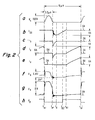
- FIGURES 2a-2h illustrate waveforms useful in explaining the operation of deflection circuit 30 of FIGURE 1. Similar symbols and numerals in FIGURES 1 and 2a-2h indicate similar items or functions.
- Retrace voltage V c of FIGURE 2a is developed across capacitor C r of FIGURE 1 as a result of energy transfer from deflection windings L H1 and L H2 via retrace current i df . Because of the autotransformer arrangement of flyback transformer T1, the retrace voltage at terminal 43 of deflection windings L H1 and L H2 is higher than voltage V c . On the other hand, current i through the collector of transistor Q1 is higher than deflection current i df .
- transformer Tl windings ratio arrangement that provides windings turns ratio of (N 1 -N 2 )/N 1 , where N 1 equals the number of turns between terminals 40 and 43 and N 2 equal the number of turns of winding section W2, between tap terminal 41 and terminal 43.
- This transformer T1 windings ratio arrangement is used for reducing voltage V c at the collector of transistor Q1 during retrace. This ratio is illustratively 0.64.
- Damper diode Dl terminates the generation of the resonant pulse voltage V c and the generation of the resonant pulse voltage developed at terminal 43 of the retrace resonant circuit formed by resonant capacitor C r and the inductance of deflection windings L H1 and L H2 -Deflection current i df in deflection windings L H1 and L H2 , continues to flow through the forward biased diode Dl, in the form of current 1 D1 of FIGURE 2b, and through forward biased zener diode Zl that is in series with the base-collector junction of transistor Ql, in the form of base current i b and reverse collector current i c of FIGURES 2c and 2d, respectively. Note that the base current waveform illustrated in FIGURE 2c is
- Zener diode Zl and transistor Q1 of FIGURE 1 assist the slow turn-on type diode D1 in conducting deflection trace current i df until a time t d of FIGURE 2d. From time t d , after diode Dl has fully turned-on, until time t ht , diode Dl of FIGURE 1 conducts the major part of deflection trace current i D1 '
- each of deflection trace current i df of FIGURE 1 and current i D1 through diode Dl become zero.
- Current begins to flow to the left from tap terminal 41 of flyback transformer primary winding W1.
- voltage V s across secondary winding W3 supplies storage charge to the base of transistor Q1 from, approximately, time t er , the beginning of trace, until time t br ' of FIGURE 2a, at the end of trace. This is so because the trace voltage across primary winding W1, causes an induced voltage V s in secondary winding W3 to be of a positive polarity at terminal 42. Voltage V s turns on diode D2 tc provide positive current i s in resistor R4 that sums with. the small current in resistor R3 to provide positive base current i b .
- the interval in which transistor Ql is supplied with positive base current overlaps the first half of trace interval t er -t ht in which diode Dl is forward biased and prior to conduction of cascode arranged FET Q2.
- the base storage charge is capable, by itself, to sustain collector current i c of FIGURE 2d between times t ht and t br '. This arrangement avoids the use of a bootstrap capacitor between the base of transistor Ql and ground to provide forward base to emitter conduction that initiates conventional transistor action.
- the amount of current that resistor R4 is required to provide during the trace interval from time t er to time t br ' to generate sufficient stored charge in the base region of transistor Ql is relatively small, less than, for example 250 milliampere, peak. This current is significantly smaller than would otherwise have been required, had the base of bipolar transistor Ql been driven normally to provide saturated, forward collector-to-emitter conduction of the deflection current of nearly six amperes peak, for example, at the collector electrode.
- the current i s thru resistor R4 may even decrease towards the end of trace, depending on the magnitude of the trace voltage V relative to the base voltage V b .
- the emitter voltage V e and thus the base voltage V b tends to increase from time t ht to time t' br due to increasing voltage drop across the channel resistance of FET Q2 produced by the increasing deflection current i df flowing therethrough.
- the negative deflection current i df flows from ground thru zener diode Z1 into the base electrode and out of the collector electrode, providing an additional mechanism for storing charge in the base region of Q1.
- positive base electrode current still flows, obtained from resistors R3 and R4 and from the forward biased zener diode Zl asting as a conventional diode. This result follows due to the negative voltage being developed at the collector electrode by the forward biased damper diode Dl.
- the positive base current flowing between time t d and time t ht is relatively small and is not illustrated in FIGURE 2c on the current scale used.
- the charge stored in the base region of transistor Q2 between times t er and t ht is sufficient by itself to maintain forward collector current i of FIGURE 2d during the later interval t ht to t br '.
- the base-collector PN junction is forward biased, producing a reverse transistor action at the emitter that generates a small negative, emitter to collector current, as illustrated in FIGURE 2e between time t d and time t ht .
- the emitter current flows from ground through the internal, oppositely poled diode, that exists in FET Q2.
- FET Q2 of FIGURE 1 is turned on by gate voltage V .
- deflection trace current i df reverses its polarity, near time t ht of FIGURES 2b and 2d, the stored charge at the base region of transistor Ql, as supplemented slightly by the currents through resistors R4 and R3, causes that current i df of FIGURE 1 flow through the collector of transistor Q1 in the form of forward collector current i of FIGURE 2d.
- Current i also flows c c through the emitter in the form of forward emitter current i of FIGURE 2e.
- both voltage V e of FIGURE 2g and voltage V b of FIGURE 2f increase as current i e of FIGURE 2e increases from time t ht to time t br '.
- FET Q2 of FIGURE 1 is turned off, as described before.
- a power supply 31 generates an ultor voltage U by rectifying the voltage at a secondary winding W2' of a high voltage flyback type of transformer T2.
- Power supply 31 includes a switched mode power supply 130 that is constructed similarly to deflection circuit 30 except that deflection windings L H1 and L H2 and their branch elements are omitted.
- Transformer T2 is analogous to flyback transformer T1 of deflection circuit 30. The iriuctance of transformer T2 then provides substantially the entire inductance that resonates with the resonating capacitance in power supply 130 to generate the narrow pulse voltage V , repeating at the 4fH rate.
- FIGURE 3 illustrates a deflection circuit output stage 30" embodying another aspect of the invention. Similar numbers and symbols in FIGURES 1 and 3 depict similar items or functions.
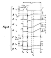
- FIGURES 4a-4h illustrate waveforms useful in explaining the operation of output stage 30" of FIGURE 3, including a controllable switching arrangement 35" similar to controllable switching arrangement 35 of FIGURE 1.
- FIGURES 4a-4h are analogous to FIGURES 2a-2h, respectively. Similar numbers and symbols in FIGURES 2a-2h and 4a-4h illustrate items or functions.
- Output stage 30" of FIGURE 3 is similar to output stage 30 of FIGURE 1 except for the exceptions noted below.
- the drain-source channel of a FET Q3 of FIGURE 3 is coupled between the base of transistor Q1 and ground.
- An inverter 27 provides a drive voltage to the gate of FET Q3 that is inverted from voltage V g supplied to the gate of FET Q2.
- FET Q3 of FIGURE 3 is conductive when FET Q2 of FIGURE 3 is nonconductive, and vice versa.
- the switching time of the current through both immediately after time t er of FIGURE 4a-4h is advantageously faster than if damper action is substantially provided by only one PN junction.
- power losses in switch 35" of FIGURE 3 are lower than if damper action is substantially provided by only one PN junction.
- the forward biased base-collector PN junction of transistor Ql causes that additional base charge is stored during the damper action.
- FET Q3 of FIGURE 3 is turned off.
- forward collector current commences at time t ht
- the charge already stored in the base region of transistor Ql is trapped, since as indicated in FIGURE 4c, after time t Q2' no significant base electrode current flows in transistor Ql.
- the base electrode current flowing when forward collector-to-emitter current flows, is insufficient, by itself, to maintain transistor Ql in a saturated state during the later portion of conduction of FET Q2.
- the stored charge in the base region is capable of sustaining collector current i of FIGURE 4d after time t ht , and of maintaining transistor Ql of FIGURE 3 in a saturated, or closed, without the need for additional positive base current.
- the arrangement of winding W3, diode D2 and resistor R4, used in deflection circuit 30 of FIGURE 1 to provide base current is eliminated from deflection circuit 30" of FIGURE 3.
Landscapes
- Details Of Television Scanning (AREA)
Applications Claiming Priority (2)
| Application Number | Priority Date | Filing Date | Title |
|---|---|---|---|
| US677522 | 1984-12-03 | ||
| US06/677,522 US4625155A (en) | 1984-12-03 | 1984-12-03 | Resonant switching apparatus using a cascode arrangement |
Publications (3)
| Publication Number | Publication Date |
|---|---|
| EP0185481A2 true EP0185481A2 (fr) | 1986-06-25 |
| EP0185481A3 EP0185481A3 (en) | 1986-10-08 |
| EP0185481B1 EP0185481B1 (fr) | 1990-06-20 |
Family
ID=24719051
Family Applications (1)
| Application Number | Title | Priority Date | Filing Date |
|---|---|---|---|
| EP85308701A Expired - Lifetime EP0185481B1 (fr) | 1984-12-03 | 1985-11-29 | Appareil commutateur à résonance utilisant un montage en cascode |
Country Status (8)
| Country | Link |
|---|---|
| US (1) | US4625155A (fr) |
| EP (1) | EP0185481B1 (fr) |
| JP (1) | JP2544720B2 (fr) |
| KR (1) | KR940011277B1 (fr) |
| CA (1) | CA1237532A (fr) |
| DE (1) | DE3578366D1 (fr) |
| HK (1) | HK94995A (fr) |
| SG (1) | SG29093G (fr) |
Cited By (1)
| Publication number | Priority date | Publication date | Assignee | Title |
|---|---|---|---|---|
| EP1359669A1 (fr) * | 2002-05-02 | 2003-11-05 | Deutsche Thomson-Brandt Gmbh | Circuit d'attaque servant à attaquer un transistor de commutation |
Families Citing this family (10)
| Publication number | Priority date | Publication date | Assignee | Title |
|---|---|---|---|---|
| US4864197A (en) * | 1987-05-14 | 1989-09-05 | Digital Equipment Corp. | Horizontal deflection circuit for video display monitor |
| US4837527A (en) * | 1987-12-23 | 1989-06-06 | Rca Licensing Corporation | Switched capacitor arrangement |
| US4777472A (en) * | 1987-12-23 | 1988-10-11 | Rca Licensing Corporation | Modified cascode amplifier |
| JPH0568178A (ja) * | 1991-09-06 | 1993-03-19 | Sony Corp | 偏向電流発生回路 |
| DE4231700C2 (de) * | 1992-09-22 | 1995-02-02 | Siemens Nixdorf Inf Syst | Horizontalendstufe einer Ablenkschaltung für die Bildröhre eines Bildschirmgerätes |
| US5939844A (en) * | 1996-05-13 | 1999-08-17 | Matsushita Electric Industrial Co., Ltd. | High-frequency horizontal deflection/high-voltage generation apparatus for cathode ray tube |
| EP0813075B1 (fr) * | 1996-06-12 | 1998-11-11 | Inter Company Computer, Engineering, Design Services, in het kort : " Concept Design", naamloze vennootschap | Dispositif de détection de proximité |
| KR100203404B1 (ko) * | 1996-11-14 | 1999-06-15 | 윤종용 | 편향구동회로 |
| US5872477A (en) * | 1997-06-13 | 1999-02-16 | Vtc Inc. | Multiplexer with CMOS break-before-make circuit |
| US6323606B1 (en) | 2000-12-27 | 2001-11-27 | Philips Electronics North America Corporation | Monitor deflection circuit |
Family Cites Families (8)
| Publication number | Priority date | Publication date | Assignee | Title |
|---|---|---|---|---|
| US3559085A (en) * | 1967-05-04 | 1971-01-26 | Iwatsu Electric Co Ltd | Transistor amplifier for high speed sweep |
| JPS5441615A (en) * | 1977-09-09 | 1979-04-03 | Hitachi Ltd | Prevention circuit for picture variation |
| JPS54127217A (en) * | 1978-03-27 | 1979-10-03 | Sony Corp | Load driver circuit |
| US4297621A (en) * | 1980-10-02 | 1981-10-27 | Sperry Corporation | Cathode ray tube beam deflection amplifier system |
| NL8100118A (nl) * | 1981-01-13 | 1982-08-02 | Philips Nv | Schakeling in een beeldweergeefinrichting voor het opwekken van een zaagtandvormige lijnafbuigstroom. |
| NL8101721A (nl) * | 1981-04-08 | 1982-11-01 | Philips Nv | Schakeling voor het opwekken van een zaagtandvormige stroom. |
| SE453241B (sv) * | 1982-04-23 | 1988-01-18 | Rca Corp | Krets for variabel horisontalavbojning, vilken krets kan astadkomma ost-vestkuddkorrigering |
| US4556825A (en) * | 1983-09-09 | 1985-12-03 | Intergraph Corporation | Switching circuit |
-
1984
- 1984-12-03 US US06/677,522 patent/US4625155A/en not_active Expired - Lifetime
-
1985
- 1985-11-22 CA CA000495992A patent/CA1237532A/fr not_active Expired
- 1985-11-29 EP EP85308701A patent/EP0185481B1/fr not_active Expired - Lifetime
- 1985-11-29 DE DE8585308701T patent/DE3578366D1/de not_active Expired - Lifetime
- 1985-12-02 KR KR1019850009030A patent/KR940011277B1/ko not_active Expired - Lifetime
- 1985-12-02 JP JP60272368A patent/JP2544720B2/ja not_active Expired - Lifetime
-
1993
- 1993-03-18 SG SG290/93A patent/SG29093G/en unknown
-
1995
- 1995-06-15 HK HK94995A patent/HK94995A/en not_active IP Right Cessation
Cited By (2)
| Publication number | Priority date | Publication date | Assignee | Title |
|---|---|---|---|---|
| EP1359669A1 (fr) * | 2002-05-02 | 2003-11-05 | Deutsche Thomson-Brandt Gmbh | Circuit d'attaque servant à attaquer un transistor de commutation |
| US6917225B2 (en) | 2002-05-02 | 2005-07-12 | Thomson Licensing S.A. | Driver circuit for driving a switching transistor |
Also Published As
| Publication number | Publication date |
|---|---|
| JPS61135278A (ja) | 1986-06-23 |
| DE3578366D1 (de) | 1990-07-26 |
| HK94995A (en) | 1995-06-23 |
| EP0185481B1 (fr) | 1990-06-20 |
| JP2544720B2 (ja) | 1996-10-16 |
| KR860005521A (ko) | 1986-07-23 |
| CA1237532A (fr) | 1988-05-31 |
| EP0185481A3 (en) | 1986-10-08 |
| US4625155A (en) | 1986-11-25 |
| KR940011277B1 (ko) | 1994-12-03 |
| SG29093G (en) | 1993-05-21 |
Similar Documents
| Publication | Publication Date | Title |
|---|---|---|
| US4625155A (en) | Resonant switching apparatus using a cascode arrangement | |
| JPH0631923B2 (ja) | 映像信号表示システム用偏向回路 | |
| US2896115A (en) | Retrace driven deflection circuit for cathode ray tubes | |
| JP3037955B2 (ja) | テレビジョン装置 | |
| US4177393A (en) | Drive circuit for a television deflection output transistor | |
| US4099101A (en) | Circuit in a television display apparatus for producing a sawtooth deflection current through a line deflection coil | |
| US4705993A (en) | Horizontal deflection circuit having a variable retrace period | |
| US3323001A (en) | Time-base circuit arrangement having transistor and scr switching elements | |
| US4301394A (en) | Horizontal deflection circuit and power supply with regulation by horizontal output transistor turn-off delay control | |
| US4193018A (en) | Deflection circuit | |
| US4362974A (en) | Commutated switched regulator with line isolation for transistor deflection | |
| KR100276494B1 (ko) | 편향 회로 장치 | |
| US4472662A (en) | Deflection circuit | |
| US3235766A (en) | Time-base circuit with self starting means | |
| GB2045564A (en) | Commutated switched regulator with line isolation for transistor deflection | |
| US4890043A (en) | Arrangement for generating a sawtooth current | |
| US4153862A (en) | Self-regulating deflection circuit with resistive diode biasing | |
| US5089756A (en) | Deflection driver in a video apparatus | |
| US5892671A (en) | Control circuit for a switching transistor using a tapped coil with oppositely wound coil parts | |
| US4163179A (en) | Circuit for providing saw-tooth current in a coil | |
| US3248598A (en) | Deflection circuit | |
| US3435280A (en) | Deflection circuit | |
| KR100651058B1 (ko) | 비디오 디스플레이 편향 장치 | |
| US5087863A (en) | Feedback arrangement in a deflection circuit | |
| KR870000819A (ko) | 텔레비젼용 전원스위치 제어 회로 |
Legal Events
| Date | Code | Title | Description |
|---|---|---|---|
| PUAI | Public reference made under article 153(3) epc to a published international application that has entered the european phase |
Free format text: ORIGINAL CODE: 0009012 |
|
| AK | Designated contracting states |
Kind code of ref document: A2 Designated state(s): DE FR GB IT |
|
| PUAL | Search report despatched |
Free format text: ORIGINAL CODE: 0009013 |
|
| AK | Designated contracting states |
Kind code of ref document: A3 Designated state(s): DE FR GB IT |
|
| 17P | Request for examination filed |
Effective date: 19870310 |
|
| 17Q | First examination report despatched |
Effective date: 19871104 |
|
| RAP1 | Party data changed (applicant data changed or rights of an application transferred) |
Owner name: RCA LICENSING CORPORATION |
|
| GRAA | (expected) grant |
Free format text: ORIGINAL CODE: 0009210 |
|
| AK | Designated contracting states |
Kind code of ref document: B1 Designated state(s): DE FR GB IT |
|
| DX | Miscellaneous (deleted) | ||
| REF | Corresponds to: |
Ref document number: 3578366 Country of ref document: DE Date of ref document: 19900726 |
|
| ITF | It: translation for a ep patent filed | ||
| ET | Fr: translation filed | ||
| PLBE | No opposition filed within time limit |
Free format text: ORIGINAL CODE: 0009261 |
|
| STAA | Information on the status of an ep patent application or granted ep patent |
Free format text: STATUS: NO OPPOSITION FILED WITHIN TIME LIMIT |
|
| 26N | No opposition filed | ||
| ITTA | It: last paid annual fee | ||
| REG | Reference to a national code |
Ref country code: GB Ref legal event code: 732E |
|
| REG | Reference to a national code |
Ref country code: GB Ref legal event code: IF02 |
|
| PGFP | Annual fee paid to national office [announced via postgrant information from national office to epo] |
Ref country code: GB Payment date: 20040924 Year of fee payment: 20 Ref country code: DE Payment date: 20040924 Year of fee payment: 20 |
|
| PGFP | Annual fee paid to national office [announced via postgrant information from national office to epo] |
Ref country code: FR Payment date: 20041117 Year of fee payment: 20 |
|
| PG25 | Lapsed in a contracting state [announced via postgrant information from national office to epo] |
Ref country code: GB Free format text: LAPSE BECAUSE OF EXPIRATION OF PROTECTION Effective date: 20051128 |
|
| REG | Reference to a national code |
Ref country code: GB Ref legal event code: PE20 |