EP0185532A2 - Montageanordnung für Oberflächenwellenanlagen - Google Patents
Montageanordnung für Oberflächenwellenanlagen Download PDFInfo
- Publication number
- EP0185532A2 EP0185532A2 EP85309125A EP85309125A EP0185532A2 EP 0185532 A2 EP0185532 A2 EP 0185532A2 EP 85309125 A EP85309125 A EP 85309125A EP 85309125 A EP85309125 A EP 85309125A EP 0185532 A2 EP0185532 A2 EP 0185532A2
- Authority
- EP
- European Patent Office
- Prior art keywords
- component
- substrate
- cradle
- cradle means
- active area
- Prior art date
- Legal status (The legal status is an assumption and is not a legal conclusion. Google has not performed a legal analysis and makes no representation as to the accuracy of the status listed.)
- Withdrawn
Links
Images


Classifications
-
- H—ELECTRICITY
- H03—ELECTRONIC CIRCUITRY
- H03H—IMPEDANCE NETWORKS, e.g. RESONANT CIRCUITS; RESONATORS
- H03H9/00—Networks comprising electromechanical or electro-acoustic elements; Electromechanical resonators
- H03H9/02—Details
- H03H9/05—Holders or supports
- H03H9/058—Holders or supports for surface acoustic wave devices
-
- H—ELECTRICITY
- H03—ELECTRONIC CIRCUITRY
- H03H—IMPEDANCE NETWORKS, e.g. RESONANT CIRCUITS; RESONATORS
- H03H9/00—Networks comprising electromechanical or electro-acoustic elements; Electromechanical resonators
- H03H9/02—Details
- H03H9/05—Holders or supports
- H03H9/10—Mounting in enclosures
- H03H9/1064—Mounting in enclosures for surface acoustic wave [SAW] devices
- H03H9/1071—Mounting in enclosures for surface acoustic wave [SAW] devices the enclosure being defined by a frame built on a substrate and a cap, the frame having no mechanical contact with the SAW device
-
- H—ELECTRICITY
- H10—SEMICONDUCTOR DEVICES; ELECTRIC SOLID-STATE DEVICES NOT OTHERWISE PROVIDED FOR
- H10W—GENERIC PACKAGES, INTERCONNECTIONS, CONNECTORS OR OTHER CONSTRUCTIONAL DETAILS OF DEVICES COVERED BY CLASS H10
- H10W72/00—Interconnections or connectors in packages
- H10W72/851—Dispositions of multiple connectors or interconnections
- H10W72/874—On different surfaces
- H10W72/884—Die-attach connectors and bond wires
-
- H—ELECTRICITY
- H10—SEMICONDUCTOR DEVICES; ELECTRIC SOLID-STATE DEVICES NOT OTHERWISE PROVIDED FOR
- H10W—GENERIC PACKAGES, INTERCONNECTIONS, CONNECTORS OR OTHER CONSTRUCTIONAL DETAILS OF DEVICES COVERED BY CLASS H10
- H10W90/00—Package configurations
- H10W90/701—Package configurations characterised by the relative positions of pads or connectors relative to package parts
- H10W90/731—Package configurations characterised by the relative positions of pads or connectors relative to package parts of die-attach connectors
- H10W90/734—Package configurations characterised by the relative positions of pads or connectors relative to package parts of die-attach connectors between a chip and a stacked insulating package substrate, interposer or RDL
-
- H—ELECTRICITY
- H10—SEMICONDUCTOR DEVICES; ELECTRIC SOLID-STATE DEVICES NOT OTHERWISE PROVIDED FOR
- H10W—GENERIC PACKAGES, INTERCONNECTIONS, CONNECTORS OR OTHER CONSTRUCTIONAL DETAILS OF DEVICES COVERED BY CLASS H10
- H10W90/00—Package configurations
- H10W90/701—Package configurations characterised by the relative positions of pads or connectors relative to package parts
- H10W90/751—Package configurations characterised by the relative positions of pads or connectors relative to package parts of bond wires
- H10W90/756—Package configurations characterised by the relative positions of pads or connectors relative to package parts of bond wires between a chip and a stacked lead frame, conducting package substrate or heat sink
Definitions
- This invention concerns mounting apparatus and packages for pressure sensitive electronic components, and particularly mounting apparatus for surface acoustic wave (SAW) devices and quartz crystals.
- SAW surface acoustic wave
- SAW surface acoustic wave
- quartz crystals have seen many applications in watches and other timepieces, and in oscillators generally.
- SAW devices are often mounted using end-loaded clamps. Although the clamps are not customarily attached in surface active regions, the fact that they are attached to a firm support in order to mount the device can cause stresses in the active regions of the SAW device.
- What is needed is a mounting system that does not introduce stresses, either thermal or mechanical into these pressure sensitive devices, and which does not contribute to surface contamination from outgassing of adhesives.
- the present invention provides apparatus for mounting an electronic component having a pressure sensitive active area, which permits the component to expand and contract with changes in temperature and which does not introduce stresses into the active area of the component.
- the apparatus includes a cradle which, when attached to a substrate, forms a partial enclosure for the component but which leaves its active area unobscured.
- the cradle is configured to have internal dimensions close to but slightly larger than the external dimensions of the component in order to constrain translational motion of the component without attaching the component to the substrate. At the same time the cradle is large enough not to introduce undesired stresses into the active area of the component.
- a packaging system is also provided wherein the bottom of the cavity of the lower portion of a standard integrated circuit package forms the substrate to be used in conjunction with the. cradle for containing the electronic component.
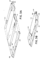
- a cradle including U-shaped end pieces 121 and 123, for holding a pressure sensitive electronic component such as a SAW device 110.
- end pieces 121 and 123 are first photopatterned on metal sheet stock, such as beryllium-copper.
- the patterned sheet stock is then precision etched and plated with a protective material, e.g., satin-nickel, from which the end pieces 121 and 123 are then formed into the shape shown in FIG. lA.
- a protective material e.g., satin-nickel
- end pieces 121 and 123 have flanges 116 and 117, and 118 and 119, respectively, which are used to weld the cradle to the bottom of a package cavity 106 as is illustrated in FIG. 2.
- tabs 113 and 115 serve to hold the SAW device in place vertically when the cradle is welded to the bottom of the cavity.
- a standard dual-in-line package is made up of a base 101 having a cavity 106 with a gold-plated attachment pad 102 therein, and a metal leadframe 105 sealed to the base 101 and to a spacer 103.
- base 101 is generally a ceramic or metallic material, however, in this embodiment ceramic is preferred, especially alumina, since it has a coefficient of thermal expansion close to that of the quartz used for the SAW device.
- ceramic is preferred, especially alumina, since it has a coefficient of thermal expansion close to that of the quartz used for the SAW device.
- Such an alumina package can be obtained from Kyocera, Inc., part number KD-75337-C.
- Flanges 116, 117, 118, and 119 are welded to attachment pad 102 using standard techniques.
- Wire or ribbon leads 109 and 108 are then attached between the SAW device 110 and the lead frame 105 using well known bonding techniques.
- a cap 111 is then sealed to spacer 103 to form an hermetic enclosure for the SAW device.
- cap 111 in the preferred construction is Kovar-plated and includes a preformed solder seal 104, typically 80% gold, 20% tin. Also the bonding surface of spacer 103 is typically gold plated. With this configuration, the attachment of the cap to the spacer is effected by placing them in contact and heating to the melting temperature of the solder in a vacuum, or in an inert atmosphere such as nitrogen or helium.
- An example of such a cap 111 can be obtained from Semi-Alloys, Inc., part number C376-21-50M-S.
- SAW device 110 Dimensions for SAW device 110 are relatively standard in the art, generally in the range of 4 mm to 20 mm long by 2 mm to 4 mm wide by 0.4 to 1 mm thicks depending on the desired resonant frequency.
- the vertical dimension of end pieces 121 and 123 is nominally about 25 microns larger than the thickness of SAW device 110 t and similarly the width of the end pieces is about 25 microns larger than the width of the SAW device.
- the end gap is generally kept to about 25 microns. This nominal clearance of 25 microns around the perimeter and vertically is not critical and can be significantly larger. The principal constraints are that the SAW device should have adequate clearance for thermal expansion during processing and that movement should be constrained "sufficiently to avoid damage to the lead attachments.
- tabs 113 and 115 are kept small, generally extending over the edge of the SAW device only as much as is necessary to hold the device in place. In this particular embodiment tabs 113 and 115 extend over the SAW device no more than about 0.4 mm. The small tab size helps to insure that the upper surface of the SAW device will remain largely unobscured in order to provide maximum flexibility for lead attachment locations, and to avoid interference with the active areas of the device. In order to better secure larger devices, it may be preferable to extend the width of the tabs by 100 to 200 microns, or even more, ,if this can be accomplished without sacrificing a significant amount of active area.
- FIGS. 3A and 3B Another embodiment is shown in FIGS. 3A and 3B.
- the cradle instead of two U-shaped end pieces, the cradle includes two L-shaped pieces'131 and 133, each covering one end and one side of SAW device 110.
- welding flanges 136, 137, 138, and 139 extend around the entire perimeter of the SAW device, and therefore permit a stronger bond to the attachment pad 102 of the package than is available in the first embodiment.
- it can accommodate SAW devices which are longer or wider than the L-shaped cradle, since the cradle need not completely surround the SAW device.
- this second embodiment is particularly well suited for larger SAW devices, and forms a more universal structure.
- tabs 143 and 145 are shown located on the sides of the SAW device 110 rather than on the ends as in Figures 1A and lB. This is to illustrate the principle that the location of the tabs is highly variable and depends on the configuration of the active area of the SAW device. Generally, the tabs are positioned to avoid interference with the active area. In this particular embodiment, the clearances between the SAW device and the cradle are substantially the same as those of the first embodiment and the general method of construction is also substantially the same.
- the pressure sensitive electronic component is not physically bonded to the restraining system and is free to expand and contract with changes in temperature. Additionally, because the component is not bonded in place, no stresses are introduced into the active area due to temperature excursions during processing. Also, the fact that no adhesives are used significantly reduces outgassing in high vacuum operations and during processing, thus curtailing surface contamination of the. pressure sensitive component. The result is stable, repeatable performance, and long-term stability for the component.
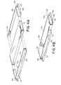
- FIGS. 4A and 4B is another embodiment of the invention implemented for illustration purposes with a SAW device 112 which is longer in extent than the L-shaped pieces 131 and 133.
- spacers 150 and 151 are placed between the L-shaped pieces and the SAW device to eliminate the gap described in the previous embodiments.
- Spacers 150 and 151 can be made of Teflon or some other relatively stable material which can act as a soft constraint to hold the SAW device in place in the cradle. The concept is to constrain the device in a secure mount which exerts only minimal pressure on the SAW device.
- the spacers 150 and 151 traverse the entire length and width of L-shaped pieces 133 and 131 respectively, and range in thickness from about 25 microns to about 125 microns.
- the motivation for this embodiment is that in practice, it can be difficult to obtain the nominal spacing of 25 microns around the perimeter of the SAW device as described in the previous embodiments, especially for large devices. As a result somewhat larger spacings, for example in the range of 50 to 75 microns can and do occur. These larger spacings in particular, and sometimes even the smaller spacings, can lead-to undesirable microphonic resonances and phase noise in the output signal from the SAW device.
- the Teflon spacers 150 and 151 by filling the gap, substantially eliminate these problems.
- FIGS. 4A and 4B Another embodiment can also be illustrated using FIGS. 4A and 4B.
- a few drops of a low vapor pressure epoxy can be used at the corner of each L-shaped piece to serve as spacers, i.e., at corners 156 and 155. (Two to five drops are generally sufficient).
- Such an epoxy is EPOTEK H-72.
- the epoxy extends along the sides and width of the L-shaped pieces only 250 to 400 microns, with a thickness in the range of about 25 to 125 microns.
- the actual volume of epoxy can vary considerably depending on the particular size of the SAW device, but the concept is to use as little epoxy as is necessary to pin the opposite corners 155 and 156 of the SAW device into the cradle, in order to ameliorate micro, phonics and phase noise often associated with a substantially unconstrained package as illustrated in FIGS. 3A and 3B.
- the cradle could be manufactured as one piece which extends around the perimeter of the pressure sensitive component.
- other devices particularly oscillators, might be packaged along with the pressure sensitive component in the same hermetic enclosure.
- the cradle can be used to constrain the motion of pressure sensitive components other than SAW devices, for example, it could also be used for quartz crystals. Therefore, the appended claims are intended to cover all such modifications, changes, and applications that fall within the true scope of the invention.
Landscapes
- Physics & Mathematics (AREA)
- Acoustics & Sound (AREA)
- Surface Acoustic Wave Elements And Circuit Networks Thereof (AREA)
- Piezo-Electric Or Mechanical Vibrators, Or Delay Or Filter Circuits (AREA)
Applications Claiming Priority (2)
| Application Number | Priority Date | Filing Date | Title |
|---|---|---|---|
| US68353084A | 1984-12-19 | 1984-12-19 | |
| US683530 | 2003-10-10 |
Publications (2)
| Publication Number | Publication Date |
|---|---|
| EP0185532A2 true EP0185532A2 (de) | 1986-06-25 |
| EP0185532A3 EP0185532A3 (de) | 1988-04-27 |
Family
ID=24744417
Family Applications (1)
| Application Number | Title | Priority Date | Filing Date |
|---|---|---|---|
| EP85309125A Withdrawn EP0185532A3 (de) | 1984-12-19 | 1985-12-16 | Montageanordnung für Oberflächenwellenanlagen |
Country Status (3)
| Country | Link |
|---|---|
| EP (1) | EP0185532A3 (de) |
| JP (1) | JPS61150405A (de) |
| CA (1) | CA1271556A (de) |
Cited By (2)
| Publication number | Priority date | Publication date | Assignee | Title |
|---|---|---|---|---|
| EP0430652A3 (en) * | 1989-11-28 | 1991-07-24 | Tektronix, Inc. | Damped cradle for saw device |
| EP0520270A1 (de) * | 1991-06-28 | 1992-12-30 | AME Space A/S | Mittel zum Montieren eines länglichen Körpers |
Families Citing this family (1)
| Publication number | Priority date | Publication date | Assignee | Title |
|---|---|---|---|---|
| AT508537B1 (de) | 2009-07-16 | 2011-04-15 | Mahle Int Gmbh | Plattenwärmetauscher mit mehreren übereinander gestapelten platten |
Family Cites Families (5)
| Publication number | Priority date | Publication date | Assignee | Title |
|---|---|---|---|---|
| JPS5847885B2 (ja) * | 1976-01-29 | 1983-10-25 | セイコーインスツルメンツ株式会社 | 振動子の支持構造 |
| JPS5499589A (en) * | 1978-01-23 | 1979-08-06 | Citizen Watch Co Ltd | Thickness slip piezoelectric oscillator |
| FR2474254A2 (fr) * | 1979-01-31 | 1981-07-24 | Composants Electro Ste Fse | Perfectionnement a un resonateur a cristal comprenant un corps cristallin parallelepipedique |
| US4398117A (en) * | 1981-03-23 | 1983-08-09 | Sperry Corporation | Bellows support for surface acoustic wave device |
| JPS57162815A (en) * | 1981-03-31 | 1982-10-06 | Fujitsu Ltd | Quartz oscillator |
-
1985
- 1985-12-10 CA CA000497265A patent/CA1271556A/en not_active Expired - Fee Related
- 1985-12-16 EP EP85309125A patent/EP0185532A3/de not_active Withdrawn
- 1985-12-19 JP JP60286830A patent/JPS61150405A/ja active Pending
Cited By (3)
| Publication number | Priority date | Publication date | Assignee | Title |
|---|---|---|---|---|
| EP0430652A3 (en) * | 1989-11-28 | 1991-07-24 | Tektronix, Inc. | Damped cradle for saw device |
| EP0520270A1 (de) * | 1991-06-28 | 1992-12-30 | AME Space A/S | Mittel zum Montieren eines länglichen Körpers |
| US5323081A (en) * | 1991-06-28 | 1994-06-21 | Ame Space As | Surface acoustic wave device clamped within housing |
Also Published As
| Publication number | Publication date |
|---|---|
| CA1271556A (en) | 1990-07-10 |
| JPS61150405A (ja) | 1986-07-09 |
| EP0185532A3 (de) | 1988-04-27 |
Similar Documents
| Publication | Publication Date | Title |
|---|---|---|
| US4845397A (en) | Constraining mount system for surface acoustic wave devices | |
| CN102355226B (zh) | 音叉型压电振动片及音叉型压电振子 | |
| US5250870A (en) | Ultra-thin surface mount crystal package | |
| EP1535350B1 (de) | Anbringstrukturen für kristallresonatoren mit geringer beschleunigungsempfindlichkeit | |
| US8350449B2 (en) | Quartz crystal device using at-cut quartz substrate and manufacturing the same | |
| JP2006279872A (ja) | 圧電振動子及びその製造方法並びにその圧電振動子を用いた圧電発振器の製造方法 | |
| JP5668392B2 (ja) | 圧電振動素子、圧電振動子及び圧電発振器 | |
| US7116039B2 (en) | Crystal unit and holding structure of crystal unit | |
| EP0185532A2 (de) | Montageanordnung für Oberflächenwellenanlagen | |
| KR100699586B1 (ko) | 수정발진기 | |
| US9041271B2 (en) | Crystal device | |
| US11293755B2 (en) | Vibrator device | |
| US11309864B2 (en) | Piezoelectric resonator unit and method for manufacturing the piezoelectric resonator unit | |
| JP5838694B2 (ja) | 物理量検出器、物理量検出デバイス及び電子機器 | |
| JP5712755B2 (ja) | 加速度検出器、加速度検出デバイス及び電子機器 | |
| EP0430652A2 (de) | Gedämpfte Lagerung für Oberflächenwellenanordnung | |
| JP2012175405A (ja) | 圧電振動素子、圧電振動子、圧電発振器及び電子機器 | |
| GB1568985A (en) | Thin and small sized piezo-electric oscilator | |
| JPH0259648B2 (de) | ||
| JP7552967B2 (ja) | 半導体パッケージ用ステム | |
| CN121461924A (zh) | 温度传感器内置型的晶体振动器 | |
| US20240219179A1 (en) | Angular Velocity Sensor | |
| US20230247907A1 (en) | Vibrator Device | |
| JP7312060B2 (ja) | 表面実装型水晶振動子付き回路基板 | |
| KR100609120B1 (ko) | 수정발진기용 세라믹 패키지 |
Legal Events
| Date | Code | Title | Description |
|---|---|---|---|
| PUAI | Public reference made under article 153(3) epc to a published international application that has entered the european phase |
Free format text: ORIGINAL CODE: 0009012 |
|
| AK | Designated contracting states |
Kind code of ref document: A2 Designated state(s): DE FR GB NL |
|
| PUAL | Search report despatched |
Free format text: ORIGINAL CODE: 0009013 |
|
| AK | Designated contracting states |
Kind code of ref document: A3 Designated state(s): DE FR GB NL |
|
| STAA | Information on the status of an ep patent application or granted ep patent |
Free format text: STATUS: THE APPLICATION IS DEEMED TO BE WITHDRAWN |
|
| 18D | Application deemed to be withdrawn |
Effective date: 19880526 |
|
| RIN1 | Information on inventor provided before grant (corrected) |
Inventor name: SANG, EMMANUEL Inventor name: HERRICK, GEOFFREY C. |