EP0185572B1 - Halbleiterspeicher mit in Blöcken unterteilten Bitleitungen - Google Patents
Halbleiterspeicher mit in Blöcken unterteilten Bitleitungen Download PDFInfo
- Publication number
- EP0185572B1 EP0185572B1 EP85402247A EP85402247A EP0185572B1 EP 0185572 B1 EP0185572 B1 EP 0185572B1 EP 85402247 A EP85402247 A EP 85402247A EP 85402247 A EP85402247 A EP 85402247A EP 0185572 B1 EP0185572 B1 EP 0185572B1
- Authority
- EP
- European Patent Office
- Prior art keywords
- block
- sense amplifier
- bit lines
- data bus
- blocks
- Prior art date
- Legal status (The legal status is an assumption and is not a legal conclusion. Google has not performed a legal analysis and makes no representation as to the accuracy of the status listed.)
- Expired - Lifetime
Links
Images



Classifications
-
- G—PHYSICS
- G11—INFORMATION STORAGE
- G11C—STATIC STORES
- G11C11/00—Digital stores characterised by the use of particular electric or magnetic storage elements; Storage elements therefor
- G11C11/21—Digital stores characterised by the use of particular electric or magnetic storage elements; Storage elements therefor using electric elements
- G11C11/34—Digital stores characterised by the use of particular electric or magnetic storage elements; Storage elements therefor using electric elements using semiconductor devices
-
- G—PHYSICS
- G11—INFORMATION STORAGE
- G11C—STATIC STORES
- G11C11/00—Digital stores characterised by the use of particular electric or magnetic storage elements; Storage elements therefor
- G11C11/21—Digital stores characterised by the use of particular electric or magnetic storage elements; Storage elements therefor using electric elements
- G11C11/34—Digital stores characterised by the use of particular electric or magnetic storage elements; Storage elements therefor using electric elements using semiconductor devices
- G11C11/40—Digital stores characterised by the use of particular electric or magnetic storage elements; Storage elements therefor using electric elements using semiconductor devices using transistors
- G11C11/401—Digital stores characterised by the use of particular electric or magnetic storage elements; Storage elements therefor using electric elements using semiconductor devices using transistors forming cells needing refreshing or charge regeneration, i.e. dynamic cells
- G11C11/4063—Auxiliary circuits, e.g. for addressing, decoding, driving, writing, sensing or timing
- G11C11/407—Auxiliary circuits, e.g. for addressing, decoding, driving, writing, sensing or timing for memory cells of the field-effect type
- G11C11/4076—Timing circuits
-
- G—PHYSICS
- G11—INFORMATION STORAGE
- G11C—STATIC STORES
- G11C11/00—Digital stores characterised by the use of particular electric or magnetic storage elements; Storage elements therefor
- G11C11/21—Digital stores characterised by the use of particular electric or magnetic storage elements; Storage elements therefor using electric elements
- G11C11/34—Digital stores characterised by the use of particular electric or magnetic storage elements; Storage elements therefor using electric elements using semiconductor devices
- G11C11/40—Digital stores characterised by the use of particular electric or magnetic storage elements; Storage elements therefor using electric elements using semiconductor devices using transistors
-
- G—PHYSICS
- G11—INFORMATION STORAGE
- G11C—STATIC STORES
- G11C11/00—Digital stores characterised by the use of particular electric or magnetic storage elements; Storage elements therefor
- G11C11/21—Digital stores characterised by the use of particular electric or magnetic storage elements; Storage elements therefor using electric elements
- G11C11/34—Digital stores characterised by the use of particular electric or magnetic storage elements; Storage elements therefor using electric elements using semiconductor devices
- G11C11/40—Digital stores characterised by the use of particular electric or magnetic storage elements; Storage elements therefor using electric elements using semiconductor devices using transistors
- G11C11/401—Digital stores characterised by the use of particular electric or magnetic storage elements; Storage elements therefor using electric elements using semiconductor devices using transistors forming cells needing refreshing or charge regeneration, i.e. dynamic cells
- G11C11/4063—Auxiliary circuits, e.g. for addressing, decoding, driving, writing, sensing or timing
- G11C11/407—Auxiliary circuits, e.g. for addressing, decoding, driving, writing, sensing or timing for memory cells of the field-effect type
- G11C11/409—Read-write [R-W] circuits
- G11C11/4091—Sense or sense/refresh amplifiers, or associated sense circuitry, e.g. for coupled bit-line precharging, equalising or isolating
-
- G—PHYSICS
- G11—INFORMATION STORAGE
- G11C—STATIC STORES
- G11C11/00—Digital stores characterised by the use of particular electric or magnetic storage elements; Storage elements therefor
- G11C11/21—Digital stores characterised by the use of particular electric or magnetic storage elements; Storage elements therefor using electric elements
- G11C11/34—Digital stores characterised by the use of particular electric or magnetic storage elements; Storage elements therefor using electric elements using semiconductor devices
- G11C11/40—Digital stores characterised by the use of particular electric or magnetic storage elements; Storage elements therefor using electric elements using semiconductor devices using transistors
- G11C11/401—Digital stores characterised by the use of particular electric or magnetic storage elements; Storage elements therefor using electric elements using semiconductor devices using transistors forming cells needing refreshing or charge regeneration, i.e. dynamic cells
- G11C11/4063—Auxiliary circuits, e.g. for addressing, decoding, driving, writing, sensing or timing
- G11C11/407—Auxiliary circuits, e.g. for addressing, decoding, driving, writing, sensing or timing for memory cells of the field-effect type
- G11C11/409—Read-write [R-W] circuits
- G11C11/4097—Bit-line organisation, e.g. bit-line layout, folded bit lines
Definitions
- the present invention relates to a semiconductor memory device having a plurality of memory cells arranged in a matrix formed by word lines and bit lines connected to a data bus, and more particularly to a semiconductor memory device wherein the bit lines are divided into a plurality of blocks each including a plurality of memory cells, a sense amplifier and a switching element inserted into each bit line.
- Memory devices having a still larger memory capacity are proposed, with the result that the number of memory cells increases considerably with many word lines and bit lines connected to the memory cells. Accordingly, the stray capacitance distributed along the word and bit lines increases, which lowers the operation speed of the memory device.
- Each block includes a plurality of memory cells, a sense amplifier and a switching element inserted into each bit line.
- Means are provided which are responsive to the selection of a memory cell to be accessed -for activating only the sense amplifier of the block containing the selected memory cell.
- the switching elements are controlled after activation of the sense amplifier of the selected block (i.e. the block containing the selected memory cell) to make ON only the switching elements of the selected block and of each other block eventually located between the selected block and the data bus.
- the object of the invention is to improve such semiconductor memory devices by allowing a high operation speed while reducing the power consumption.
- Another object of the invention is also to increase the operation reliability of the semiconductor memory device.
- the sense amplifiers in the farthest blocks from the data bus have the highest driving ability to amplify the voltage difference in enough short time despite the load capacitance along the bit lines, while the nearest blocks from the data bus have the lowest driving ability to avoid unnecessary power consumption.
- Sense amplifiers having different driving abilities can be obtained by using MOS (metal-oxide- semiconductor) transistors having different channel sizes.
- MOS metal-oxide- semiconductor
- a conventional memory device having a memory capacity of 64 kilo (K) bits or 256 K bits
- the memory cells are arranged in a matrix as shown in Fig.1.
- reference symbols Coo, C 01 , ---, C on designate the memory cells in 0-th column
- Each memory cell is located at the cross point of respective word line and pair of bit lines.
- the reference symbols WDo, WD 1 , ---, and WD n denote the 0-th, 1-st, ---, and n-th word line, respectively, and BL o , BL o ; BL 1 , BL 1;---; BL;, BL i ; ---; BL n , BL n denote the 0-th, 1-st, ---, i-th, ---, and n-th pair of bit lines, respectively.
- the pairs of bit lines have respective comumn decoders CDo, CO 1 , ---, CD;, ---, CD n .
- the word lines have respective word decoders WDo, WD 1 , ---, WD n .
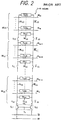
- each block comprises a pair of divided bit lines, a plurality of memory cells, a block sense amplifier, and a pair of switching elements.
- block BK ik has a pair of divided bit lines BL ik , BL ik , a plurality of memory cells C ik0 , C ik1' ---, and C ikm , a block sense amplifier SA ik , and a pair of switching elements S ik , S ik .
- a corresponding one of block select signals BS io , BS i1 , ---, and BS ik is applied to the block sense amplifier of the block containing the selected memory cell in order to activate said block amplifier of the selected block. Then, the selected block sense amplifier amplifies the data signal stored in the selected memory cell. Pairs of switching elements s i0 , s i0; S i1 , S i1 ; ---; and S ik , S ik are inserted in the pairs of bit lines in the blocks B io , B i1 , --, B ik , respectively, for connecting the blocks in series.
- Column decoder CD i is inserted between the block (BK ik ) which is nearest to the pair of bus lines DB, DB ,and the pair of bus lines DB, DB .
- transfer gates Q i1 and Q; 2 provided in the column decoder CD are set to the ON state for sending the data signal which is amplified by the selected block sense amplifier to the pair of bus lines DB, DB .
- Fig. 3(a) shows a pre-charge circuit PRE i0 which comprises transistors Q i01 , Q i02 , and Q i03 for applying equal pre-charging potential (V cc - V th ) to the pair of bit lines BL io , BL i0 when a pre-charge signal p is applied to the gates of transistors Q i01 , Q i02 , and Q i03 .
- the transistor Q i04 shown in Fig.3(b) forms the switching element S i0 or S i0 shown in Fig. 2; transistor Q i04 becomes ON when a clock signal ⁇ is applied to its gate.
- FIG. 3(c) shows another type of switching element which consists of a transistor Q i04 which is similar to that in Fig. 3(b) and of a transistor Q i05 which is connected in parallel to transistor Q i04 and is of a conduction type reverse to the one of transistor Q i04 ; the switching element of Fig. 3(c) becomes ON when clock signals ⁇ , ⁇ are simultaneously applied to the gates of the transistors Q i04 and Q i05 , respectively.
- the operation of the circuit of Fig. 2 includes the following sequential steps: (1) one word line is selected by a word line select signal Xo, X 1 , ---, or X n (see Fig. 1); for example, word WLo is selected by the word line select signal X o ; (2) one column is selected by a column select signal Y o , Yi, ---, or Y n ; for example, column i is selected by the column select signal Y i ; (3) the memory cell located at the cross point of the selected word line and column is selected; for example, memory cell C ioo in block BK i0 is selected; (4) one block select signal is provided when a word line and a column have been selected, corresponding to the block containing the selected cell; for example, block select signal BS i0 is provided; (5) the block sense amplifier of the selected block is activated by the block select signal, so that a voltage difference appearing between the bit lines in the selected block is amplified; for example, block sense amplifier SA
- step (6) it is not necessary that "all switching elements" be made ON. As already known, it is sufficient to set in the ON state the switching elements in the selected block and in the blocks located between the selected block and the column decoder CD;.
- all other block sense amplifiers may be activated after the selected block sense amplifier has been activated and the switching elements have been made ON.
- the load capacitance for the sense amplifier can be kept small at the first time when the block sense amplifier in the selected block is activated.
- the load capacitance for the selected block sense amplifier increases; for example in Fig. 2, when block BK io is selected and sense amplifier SA i0 is activated and the switching elements serially connect all the blocks, the load capacitance becomes the total capacitance along the whole bit lines in column i.
- the sense amplifier in the farthest block from the data bus for example sense amplifier SA i0 in block BK i0 , must have a great enough driving ability to amplify the voltage difference in a short enough time.
- all the sense amplifiers have an equal driving ability,and if the sense amplifier in the nearest block from the data bus, for example sense amplifier SA ik in block Bk ik , is selected, this sense amplifier (SA ik ) wastes too much power.
- Fig. 4 is a block and circuit diagram of a column part of a memory device embodying the present invention.
- the block and circuit diagram in Fig.4 has the same constitution as that of the block and circuit diagram of Fig.2, and, in Figs. 2 and 4, the parts having the same reference symbols function equally.
- VSA i0 , VSA il , ---, VSA ik designate the block sense amplifiers which are similar to the block sense amplifiers in Fig.2 but have individual driving abilities different from each other such that the block sense amplifier in the farthest block from column decoder CD i or data bus DB, DB has the maximum driving ability and the block sense amplifier in the block nearest to data bus DB, DB has the minimum driving ability.
- the memory device functions as follows. (1) the i-th column is selected when column select signal Y i is applied to column decoder CD i (see Fig.
- Switching elements S ik , S ik in the block BK ik nearest to the data bus can be omitted because they are always used.
- the above control of the switching elements is performed by modified clock signals generated by a modified clock signal generator such as the one shown in Fig. 5.
- the modified clock signal generator shown in Fig. 5 generates modified clock signals ⁇ o , ⁇ 1 , ---, and ⁇ k for controlling the setting of the respective switching elements S io , S o; S i1 , S i1 ; ---, and Si k , S ik to the ON or OFF state.
- the modified clock signals are similar to the clock signal ⁇ shown in Figs.
- the above selection of the modified clock signals is made in the modified clock signal generator by combining properly the block select signals BS io , BS i1 , ---, and BS ik .
- OR gates OG 1 , ---, OG k perform the above logic functions
- AND gates AGo, AG 1 , ---, and AG k produce the modified clock signals every time when clock signal ⁇ is applied to said AND gates.
- the OR gate OG j has a plurality of inputs receiving respectively the block select signals BS io to BS ij (j being an integer having any value from 1 to ok).
- the AND gate AGo has two inputs receiving respectively the clock signals and the block select signal while the AND gate AG j has two inputs receiving respectively the clock signal ⁇ and the output of the OR gate OG j .
- the bit lines in the selected block and the blocks located between the selected block and the data bus can be connected.
- the load capacitance of the activated sense amplifier can be reduced as much as possible; for example, when block BK i1 is selected, the stray capacitance appearing along bit lines BL io , BL i0 in block BK; o has no influence upon sense amplifier SA i0 .
- the pre-charge circuits (or bit line reset circuits) of Fig. 3(a) in said upper blocks can be controlled to be non-operative, which also contributes to saving power consumption.
- the sense amplifier in the selected block first operates, and then the switching elements in lower blocks, i. e. the blocks located between the selected block and the data bus are set to the ON state. Accordingly, when the pairs of bit lines in the lower blocks are connected to the pair of bit lines in the selected block, the voltage difference which has appeared between the bit lines in the selected block decreases due to the stray capacitance and the potential of the bit lines in the lower blocks, which causes the increase of the access time to the memory device. Accordingly, it can be said that the access time depends on the location of the selected block; for example, when the distance between the selected block and the data bus increases, the access time increases.
- the load capacitance for the sensing amplifier in the selected block is actually the sum of the stray capacitance of the lower blocks and the data bus. Therefore, when the sensing amplifier in each block has the same driving ability, as in the prior art, it becomes difficult for a sensing amplifier in a block placed far from the data bus to drive its load capacitance in a short access time. If the driving ability of the block which is the farthest from the data bus is made large enough to sufficiently shorten the access time, and if each sense amplifier must have the same large driving ability as the sense amplifier in the farthest block, this causes a waste of power when the sense amplifiers in the blocks located near the data bus are selected.
- the present invention solves this problem by providing block sense amplifiers with different driving abilities as a function of their location with respect to the data bus, the farthest block from the data bus having the highest driving ability; for example, in Fig. 4, sense amplifier VSA i0 has the maximum driving ability and the driving ability becomes smaller and smaller as the distance between the block and the data bus decreases. Then, the increase in the load capacitance can be compensated by the increase in the driving ability so that the access time for all the blocks can be equalized.
- Fig. 6 shows a circuit diagram of a block sense amplifier with a pair of switching elements, for example in block BK io .
- Q i and Q 2 are p-channel MOS (Metal Oxide Semiconductor) transistors, while Q 3 , Q 4 , and Q 5 are n-channel MOS transistors.
- V ss is a low power supply voltage (usually ground (GND)) and V cc is a high power supply voltage.
- BS is a block select terminal, and BL io , BL i0, BLil, BL i1 ; are divided bit lines as in Fig.2.
- Transistors Q 1 and Q 3 , and transistors Q 2 and Q 4 compose two CMOS (Complementary MOS) inverters, respectively, and the two CMOS invertors intersect each other to form a flop-flop circuit.
- the circuit formed by the two parallel connected CMOS invertors is serially connected with transistor Q 5 between V cc and V ss .
- Transistor Q 5 is set to the ON state upon reception of a block select signal on the terminal BS, activating the sense amplifier.
- Q 6 and Q 7 are n-channel MOS transistors which form the switching elements into the bit lines and similar to the ones shown in Fig.3(b).
- Figs. 7(a) and (b) show plan views of the IC (Integrated semiconductor Circuit) pattern for the circuit of Fig.6, respectively when the block sense amplifier has the maximum driving ability, and when the block sense amplifier has the minimum driving ability.
- each dotted area is a pattern for a limited diffusion zone
- each shadowed area is a pattern for a gate material made of Poly-Silicon
- each X marked portion shows a window for AI (Aluminum) contact
- each area enclosed by a thick line is a pattern for an AI wiring.
- w 1 is the channel size for transistors Q 1 and Q 2
- w 2 is the channel size for transistors Q 3 and Q 4
- w 3 is the channel size for transistor Qs.
- the memory device is in the class having M-bit memory capacity and the channel size for the transistors of a middle block sense amplifier, i.e.
- the block sense amplifier of the block located at the middle of the column is set as a standard size
- the ratio between each channel size and the respective standard size may be as follows: when the driving ability has its maximum value,w l , W2 , and W3 are longer than the respective standard sizes by as much as forty percent and when the driving ability has its minimum value, w 1 , w 2 , and w 3 are smaller than the respective standard sizes by sixty percent.
- Fig.8 is a time chart illustrating the operation of the memory device shown in Fig. 4.
- a pre-charge signal p is generated so that all the pairs of bit lines BL io , BL o; BL i1 , BL i1 ; --- ; and BL ik , BL ik shown in Fig.4 are charged to an equal value, such as V cc - V th for example.
- word line WLo is selected (see Figs.
- the potential on the bit lines in all other non-selected blocks is a middle value of the pre-charge potential; accordingly, the H side of the bit lines BL io , BL i0 in selected block BK i0 decreases while the T thereof increases.
- the driving ability of sense amplifier VSA i0 is great, the voltage difference appearing on bit lines BL io , BL i0 (and also on the other bit lines in the non-selected blocks) rapidly returns back to the value it had just before t 3 though the load for sense amplifier BSA i0 has the maximum value.
Landscapes
- Engineering & Computer Science (AREA)
- Computer Hardware Design (AREA)
- Microelectronics & Electronic Packaging (AREA)
- Dram (AREA)
- Static Random-Access Memory (AREA)
Claims (2)
Applications Claiming Priority (4)
| Application Number | Priority Date | Filing Date | Title |
|---|---|---|---|
| JP24580384A JPH0652635B2 (ja) | 1984-11-20 | 1984-11-20 | 半導体記憶装置 |
| JP59245801A JPS61123093A (ja) | 1984-11-20 | 1984-11-20 | 半導体記憶装置 |
| JP245803/84 | 1984-11-20 | ||
| JP245801/84 | 1984-11-20 |
Publications (3)
| Publication Number | Publication Date |
|---|---|
| EP0185572A2 EP0185572A2 (de) | 1986-06-25 |
| EP0185572A3 EP0185572A3 (en) | 1988-04-20 |
| EP0185572B1 true EP0185572B1 (de) | 1991-04-03 |
Family
ID=26537410
Family Applications (1)
| Application Number | Title | Priority Date | Filing Date |
|---|---|---|---|
| EP85402247A Expired - Lifetime EP0185572B1 (de) | 1984-11-20 | 1985-11-20 | Halbleiterspeicher mit in Blöcken unterteilten Bitleitungen |
Country Status (4)
| Country | Link |
|---|---|
| US (1) | US4730280A (de) |
| EP (1) | EP0185572B1 (de) |
| KR (1) | KR900005667B1 (de) |
| DE (1) | DE3582415D1 (de) |
Families Citing this family (27)
| Publication number | Priority date | Publication date | Assignee | Title |
|---|---|---|---|---|
| US4731747A (en) * | 1986-04-14 | 1988-03-15 | American Telephone And Telegraph Company, At&T Bell Laboratories | Highly parallel computation network with normalized speed of response |
| US5132930A (en) * | 1986-07-31 | 1992-07-21 | Mitsubishi Denki Kabushiki Kaisha | CMOS dynamic memory device having multiple flip-flop circuits selectively coupled to form sense amplifiers specific to neighboring data bit lines |
| EP0523756A3 (en) * | 1986-08-15 | 1993-06-09 | Nec Corporation | Static random access memory having bi-cmos construction |
| JPH07118193B2 (ja) * | 1986-09-18 | 1995-12-18 | 富士通株式会社 | 半導体記憶装置 |
| ATE73255T1 (de) * | 1986-11-18 | 1992-03-15 | Siemens Ag | Digitalverstaerkeranordnung in integrierten schaltungen. |
| KR890002812B1 (ko) * | 1986-11-28 | 1989-07-31 | 삼성전자 주식회사 | 씨모오스 디램에서 레이아웃이 최적화된 감지증폭기 |
| JPS63149900A (ja) * | 1986-12-15 | 1988-06-22 | Toshiba Corp | 半導体メモリ |
| JPH0799627B2 (ja) * | 1987-01-23 | 1995-10-25 | 松下電器産業株式会社 | 半導体メモリの書き込み読み出し回路 |
| JPH07107797B2 (ja) * | 1987-02-10 | 1995-11-15 | 三菱電機株式会社 | ダイナミツクランダムアクセスメモリ |
| US4980863A (en) * | 1987-03-31 | 1990-12-25 | Kabushiki Kaisha Toshiba | Semiconductor memory device having switching circuit for coupling together two pairs of bit lines |
| US4807195A (en) * | 1987-05-18 | 1989-02-21 | International Business Machines Corporation | Apparatus and method for providing a dual sense amplifier with divided bit line isolation |
| JP2828630B2 (ja) * | 1987-08-06 | 1998-11-25 | 三菱電機株式会社 | 半導体装置 |
| JPH07105137B2 (ja) * | 1987-11-17 | 1995-11-13 | 日本電気株式会社 | 半導体メモリ |
| KR890010917A (ko) * | 1987-12-28 | 1989-08-11 | 다니이 아끼오 | 낮은 첨두전류로 작동하는 반도체 메모리 |
| JPH0235765A (ja) * | 1988-07-26 | 1990-02-06 | Nec Corp | 半導体集積回路装置 |
| DE3937068C2 (de) * | 1988-11-07 | 1994-10-06 | Toshiba Kawasaki Kk | Dynamische Halbleiterspeicheranordnung |
| JPH07105140B2 (ja) * | 1988-12-16 | 1995-11-13 | 日本電気株式会社 | 半導体メモリ |
| US5293563A (en) * | 1988-12-29 | 1994-03-08 | Sharp Kabushiki Kaisha | Multi-level memory cell with increased read-out margin |
| JPH03176891A (ja) * | 1989-12-04 | 1991-07-31 | Nec Corp | 半導体記憶装置 |
| US4972374A (en) * | 1989-12-27 | 1990-11-20 | Motorola, Inc. | Output amplifying stage with power saving feature |
| US5226014A (en) * | 1990-12-24 | 1993-07-06 | Ncr Corporation | Low power pseudo-static ROM |
| JP3533227B2 (ja) * | 1992-09-10 | 2004-05-31 | 株式会社日立製作所 | 半導体記憶装置 |
| US5515315A (en) * | 1993-12-24 | 1996-05-07 | Sony Corporation | Dynamic random access memory |
| US5666320A (en) * | 1995-12-20 | 1997-09-09 | International Business Machines Corporation | Storage system |
| US6552932B1 (en) * | 2001-09-21 | 2003-04-22 | Sandisk Corporation | Segmented metal bitlines |
| KR100564607B1 (ko) * | 2004-01-29 | 2006-03-28 | 삼성전자주식회사 | 태퍼드 lio 센스 앰프를 사용하는 반도체 메모리 장치 |
| TWI493568B (zh) * | 2013-08-19 | 2015-07-21 | Ind Tech Res Inst | 記憶體裝置 |
Family Cites Families (7)
| Publication number | Priority date | Publication date | Assignee | Title |
|---|---|---|---|---|
| DE2647394C2 (de) * | 1976-10-20 | 1978-11-16 | Siemens Ag, 1000 Berlin Und 8000 Muenchen | MOS-Halbleiterspeicherbaustein |
| US4286178A (en) * | 1978-06-12 | 1981-08-25 | Texas Instruments Incorporated | Sense amplifier with dual parallel driver transistors in MOS random access memory |
| US4287576A (en) * | 1980-03-26 | 1981-09-01 | International Business Machines Corporation | Sense amplifying system for memories with small cells |
| JPS57198592A (en) * | 1981-05-29 | 1982-12-06 | Hitachi Ltd | Semiconductor memory device |
| EP0101884A3 (de) * | 1982-07-21 | 1987-09-02 | Hitachi, Ltd. | Monolithischer Halbleiterspeicher |
| JPH0670878B2 (ja) * | 1982-11-30 | 1994-09-07 | 富士通株式会社 | 半導体記憶装置 |
| US4542483A (en) * | 1983-12-02 | 1985-09-17 | At&T Bell Laboratories | Dual stage sense amplifier for dynamic random access memory |
-
1985
- 1985-11-18 KR KR1019850008611A patent/KR900005667B1/ko not_active Expired
- 1985-11-18 US US06/798,783 patent/US4730280A/en not_active Expired - Lifetime
- 1985-11-20 DE DE8585402247T patent/DE3582415D1/de not_active Expired - Lifetime
- 1985-11-20 EP EP85402247A patent/EP0185572B1/de not_active Expired - Lifetime
Also Published As
| Publication number | Publication date |
|---|---|
| KR900005667B1 (ko) | 1990-08-03 |
| KR860004409A (ko) | 1986-06-20 |
| DE3582415D1 (de) | 1991-05-08 |
| EP0185572A3 (en) | 1988-04-20 |
| US4730280A (en) | 1988-03-08 |
| EP0185572A2 (de) | 1986-06-25 |
Similar Documents
| Publication | Publication Date | Title |
|---|---|---|
| EP0185572B1 (de) | Halbleiterspeicher mit in Blöcken unterteilten Bitleitungen | |
| EP1349170B1 (de) | Leseverstärker | |
| EP0384673B1 (de) | Speicheranordnungen | |
| KR950009877B1 (ko) | 복수의 셀블록으로 분할된 셀어레이를 구비한 반도체 기억장치 | |
| US4931994A (en) | Static semiconductor memory with section and block sense amplifiers | |
| US4817057A (en) | Semiconductor memory device having improved precharge scheme | |
| KR970029841A (ko) | 감소 칩 영역을 가진 반도체 메모리 소자 | |
| US7349274B2 (en) | Precharge circuit and method employing inactive weak precharging and equalizing scheme and memory device including the same | |
| US6711088B2 (en) | Semiconductor memory device | |
| JPH0422318B2 (de) | ||
| US4003035A (en) | Complementary field effect transistor sense amplifier for one transistor per bit ram cell | |
| EP0388176B1 (de) | Halbleiter-Speichereinrichtung | |
| US5148399A (en) | Sense amplifier circuitry selectively separable from bit lines for dynamic random access memory | |
| US6845049B2 (en) | Semiconductor memory device including a delaying circuit capable of generating a delayed signal with a substantially constant delay time | |
| US4625298A (en) | Semiconductor memory device | |
| KR100257911B1 (ko) | 반도체 기억장치 | |
| JP3136483B2 (ja) | 半導体メモリ装置 | |
| US5982692A (en) | Bit line boost amplifier | |
| US6067264A (en) | High speed semiconductor memory device | |
| JP4272592B2 (ja) | 半導体集積回路 | |
| EP0451000B1 (de) | Halbleiter-Speichereinrichtung mit verbesserter Kontrollfunktion für Datenbusse | |
| EP0509497B1 (de) | Dynamische Direktzugriffspeicheranordnung mit seriellaktivierten Abfühlverstärkerschaltungsarrays | |
| KR100388217B1 (ko) | 반도체 메모리 | |
| KR950008672B1 (ko) | 입/출력 라인사이에서 전위차를 억제하기 위한 클램핑 회로를 구비한 반도체 메모리 장치 | |
| EP0350860B1 (de) | Halbleiterspeicher mit verbesserten Abfühlverstärkern |
Legal Events
| Date | Code | Title | Description |
|---|---|---|---|
| PUAI | Public reference made under article 153(3) epc to a published international application that has entered the european phase |
Free format text: ORIGINAL CODE: 0009012 |
|
| AK | Designated contracting states |
Kind code of ref document: A2 Designated state(s): DE FR GB |
|
| PUAL | Search report despatched |
Free format text: ORIGINAL CODE: 0009013 |
|
| AK | Designated contracting states |
Kind code of ref document: A3 Designated state(s): DE FR GB |
|
| 17P | Request for examination filed |
Effective date: 19881010 |
|
| 17Q | First examination report despatched |
Effective date: 19900504 |
|
| GRAA | (expected) grant |
Free format text: ORIGINAL CODE: 0009210 |
|
| AK | Designated contracting states |
Kind code of ref document: B1 Designated state(s): DE FR GB |
|
| REF | Corresponds to: |
Ref document number: 3582415 Country of ref document: DE Date of ref document: 19910508 |
|
| ET | Fr: translation filed | ||
| PLBE | No opposition filed within time limit |
Free format text: ORIGINAL CODE: 0009261 |
|
| STAA | Information on the status of an ep patent application or granted ep patent |
Free format text: STATUS: NO OPPOSITION FILED WITHIN TIME LIMIT |
|
| 26N | No opposition filed | ||
| REG | Reference to a national code |
Ref country code: GB Ref legal event code: IF02 |
|
| PGFP | Annual fee paid to national office [announced via postgrant information from national office to epo] |
Ref country code: FR Payment date: 20031110 Year of fee payment: 19 |
|
| PGFP | Annual fee paid to national office [announced via postgrant information from national office to epo] |
Ref country code: GB Payment date: 20031119 Year of fee payment: 19 |
|
| PGFP | Annual fee paid to national office [announced via postgrant information from national office to epo] |
Ref country code: DE Payment date: 20031127 Year of fee payment: 19 |
|
| PG25 | Lapsed in a contracting state [announced via postgrant information from national office to epo] |
Ref country code: GB Free format text: LAPSE BECAUSE OF NON-PAYMENT OF DUE FEES Effective date: 20041120 |
|
| PG25 | Lapsed in a contracting state [announced via postgrant information from national office to epo] |
Ref country code: DE Free format text: LAPSE BECAUSE OF NON-PAYMENT OF DUE FEES Effective date: 20050601 |
|
| GBPC | Gb: european patent ceased through non-payment of renewal fee |
Effective date: 20041120 |
|
| PG25 | Lapsed in a contracting state [announced via postgrant information from national office to epo] |
Ref country code: FR Free format text: LAPSE BECAUSE OF NON-PAYMENT OF DUE FEES Effective date: 20050729 |
|
| REG | Reference to a national code |
Ref country code: FR Ref legal event code: ST |