EP0186185A2 - Kontinuierliches Verfahren zur Herstellung metallischer Muster auf einem Dunnfilmsubstrat - Google Patents
Kontinuierliches Verfahren zur Herstellung metallischer Muster auf einem Dunnfilmsubstrat Download PDFInfo
- Publication number
- EP0186185A2 EP0186185A2 EP85116495A EP85116495A EP0186185A2 EP 0186185 A2 EP0186185 A2 EP 0186185A2 EP 85116495 A EP85116495 A EP 85116495A EP 85116495 A EP85116495 A EP 85116495A EP 0186185 A2 EP0186185 A2 EP 0186185A2
- Authority
- EP
- European Patent Office
- Prior art keywords
- film
- metal
- bath
- substrate
- circuit
- Prior art date
- Legal status (The legal status is an assumption and is not a legal conclusion. Google has not performed a legal analysis and makes no representation as to the accuracy of the status listed.)
- Withdrawn
Links
Images


Classifications
-
- C—CHEMISTRY; METALLURGY
- C25—ELECTROLYTIC OR ELECTROPHORETIC PROCESSES; APPARATUS THEREFOR
- C25D—PROCESSES FOR THE ELECTROLYTIC OR ELECTROPHORETIC PRODUCTION OF COATINGS; ELECTROFORMING; APPARATUS THEREFOR
- C25D5/00—Electroplating characterised by the process; Pretreatment or after-treatment of workpieces
- C25D5/02—Electroplating of selected surface areas
-
- H—ELECTRICITY
- H05—ELECTRIC TECHNIQUES NOT OTHERWISE PROVIDED FOR
- H05K—PRINTED CIRCUITS; CASINGS OR CONSTRUCTIONAL DETAILS OF ELECTRIC APPARATUS; MANUFACTURE OF ASSEMBLAGES OF ELECTRICAL COMPONENTS
- H05K3/00—Apparatus or processes for manufacturing printed circuits
- H05K3/10—Apparatus or processes for manufacturing printed circuits in which conductive material is applied to the insulating support in such a manner as to form the desired conductive pattern
- H05K3/18—Apparatus or processes for manufacturing printed circuits in which conductive material is applied to the insulating support in such a manner as to form the desired conductive pattern using precipitation techniques to apply the conductive material
- H05K3/181—Apparatus or processes for manufacturing printed circuits in which conductive material is applied to the insulating support in such a manner as to form the desired conductive pattern using precipitation techniques to apply the conductive material by electroless plating
-
- B—PERFORMING OPERATIONS; TRANSPORTING
- B32—LAYERED PRODUCTS
- B32B—LAYERED PRODUCTS, i.e. PRODUCTS BUILT-UP OF STRATA OF FLAT OR NON-FLAT, e.g. CELLULAR OR HONEYCOMB, FORM
- B32B2519/00—Labels, badges
- B32B2519/02—RFID tags
Definitions
- the invention relates to a process for forming electrically conductive metallic patterns on a thin polyolefin film substrate. More particularly, this invention relates to the formation of resonant RF-tuned printed circuits formed on a thin polyolefin film which are particularly useful in electronic security and article surveillance detection systems.
- a preferred special electronic tag utilizes a technology based on tuned circuits which operate in the radio frequency range.
- a a discrete inductor (L) and a discrete capacitor (C) are connected together.
- the reusable resonant tag uses discrete capacitor and inductor components which are connected to form the tuned inductor-capacitor (LC) circuit.
- the capacitor and inductor Prior to the present invention, the capacitor and inductor have been formed by conventional fabrication methods for forming printed circuits including selective use of laminated substrates having an interior dielectric layer laminated on both surfaces with a conductive composition such as aluminum or copper.
- the conductive layers are printed with an etchant resistant material in the form of the desired circuit and, after etching, the remaining conductive material is now in the form of the desired circuit.
- a conventional process is disclosed, for example, in U.S. Patent 3 913 219 and 4 369 557.
- Further examples of resonant circuit tags are disclosed in U.S. Patents 3 967 161, 4 021 705, 3 810 147 and 3 863 244. Any process for producing disposable resonant tag circuits must be capable of producing satisfactorily functioning resonant tag circuits at high volume and low cost with accurate tolerances so that uniform electrical properties are obtained from tag to tag.
- Q quality factor
- the "Q" factor is also related to the nature of the dielectric film in the resonant tag circuit which means, the dielectric loss of the substrate should be minimized to improve the "Q" factor.
- This dielectric loss is normally referred to as the dielectric dissipation factor of the capacitor.
- Many polymeric films such as polyimide film or polyester film cannot be utilized to form resonant tag circuits since their dielectric properties are inappropriate at the desired frequencies.
- the requirement for precise process control in the subtractive etching type processes serves to limit the volume production of circuits since process downtime frequently occurs when the process parameters are found to be outside of the critical process parameters necessary for producing satisfactory products.
- the use of a subtractive etching type process is also undesirable since the metal removed from the laminated substrate is lost and the cost of the process is thereby increased. This is particularly true when it is desirable to use highly conductive and expensive metals such as copper, silver or gold.
- the subtractive etching process is only commercially feasible when using less conductive, inexpensive metals such as aluminum to form the laminated substrate from which the circuits are produced.
- plastic parts such as molded plastics used for automotive parts (e.g., knobs, trim, etc.) which involves the steps of treating a plastic substrate so that it is capable of accepting a catalyst compound that promotes electroless metal deposition.
- the thus- activated plastic substrate then is immersed in an electroless metal bath to form a conductive metal coating on the substrate. Additional metal coatings can be formed on the electroless metal surface by electroplating if desired.
- the plastic substrates have a large mass and are relatively thick and therefore are capable of withstanding severe process conditions such as exposure to strong solvents and etching acids at elevated temperatures to condition the surface so that catalyst compounds can be deposited on the plastic surface relatively quickly.
- the present invention provides an additive process for forming metallic patterns on a thin polyolefin film substrate.
- the film is treated in order to deposit thereon a catalyst composition which promotes electroless deposition of metal onto one or both surfaces of the thin film polyolefin substrate with good adhesion.
- the polyolefin film is contacted with a solvent under mild conditions to plasticize the film and render it receptive to etching with an acidic etchant.
- the catalyst composition then is adsorbed onto the surface of the etched film.
- the etched film containing the catalyst composition then is printed with a negative image of the circuit pattern an electrolessly and electrolytically plated in the non-printed areas. This is referred to as the additive process (see Scheme I in Chart I).
- the printing step precedes the electroless and electrolytic plating.
- electroless plating with or without a subsequent thin electrolytic plate precedes printing, and the printed negative image of the circuit pattern, which masks the plated layers, is subsequently removed by stripping and the previously masked plated areas are removed by etching.
- the process of this invention provides advantages over the processes of the prior art since the electrolessly deposited copper is a far thinner film as compared to the metal layer in the metal-plastic laminates now utilized.
- a thin film polyolefin substrate is treated to effect adsorption of a catalyst composition on one or both surfaces of the film without materially adversely affecting the mechanical strength of the film.
- polyolefin film substrate refers to a film formed from a polymer composition having a thickness usually between about 0.5 and about 0.00254 mm. Suitable polyolefin films include polyethylene, polypropylene, polypentene polybutylene7 and copolymers or mixtures thereof.
- the pretreatment process generally involves the use of the following succession of treatment steps (a) solvent swelling, (b) etching, (c) conditioning, and (d) catalyzing.
- Solvent swelling is conducted to plasticize the polyolefin film thereby to facilitate etching which provides a microporous surface, but without permanently adversely affecting the mechanical properties of the film. That is, the film should retain virtually all of its mechanical strength upon removal of the plasticizer therefrom. The degree of plasticizing should be controlled so that the film can be etched subsequently without adversely affecting its mechanical properties.
- the particular solvent composition employed depends upon the particular polyolefin film being treated. For example, with polypropylene, turpentine based emulsions are desirable and such solvent systems are disclosed in U.S. Patent 3 579 365. Usually the film is immersed for a time between 1 and 10 minutes. The solvent- treated film then is rinsed prior to etching to remove excess solvent.
- the polyolefin thin film then is etched to provide attraction sites for subsequent catalytic metal deposition and to provide microvoids for increasing adhesion of the metal- plating layer to be subsequently applied.
- Etching involves solvating one or more phases of the polyolefin surface to form microvoids and chemically modifying the remaining resin to provide attraction sites for catalytic metal deposition. It has been found that precise control of this step is essential in the process of this invention in order to render the surface sufficiently adherent to the subsequent metal layer without destroying film mechanical integrity.
- the micro-pitted film surface facilitates excellent adhesion on subsequently applied metal so that the circuits so formed do not peel or flake from the film.
- the conditions of etching must be controlled to maintain the mechanical integrity of the film while effecting sufficient surface modification to promote subsequent electroless metal deposition so that the plating is tightly adhered to the film without being delaminated. Secure bonds to the deposited metal are achieved by microroughening the substrate, such as by the use of controlled acidic chromium oxidation, prior to plating.
- the preferred etching composition is a mixture of chromic acid and sulfuric acid wherein the weight ratio of chromic acid to sulfuric acid is between about 1 to 2 and 1 to 5, the etching solution is between about 40 and 50° Baume, preferably between about 41° and 48° Baume .
- the etchant bath should be maintained between about 60° and 90°C, preferably between about 75°C and 85 0 C.
- a fluorochemical surfactant additive in the chromic / sulfuric acid etching bath at concentrations between 10 and 1000 ppm (parts per million), preferably 100-500 ppm, which increases film surface wetting by the etching solution and promotes a more even etching profile across the film surfaces.
- fluorochemical surfactants are described in U.S. Patent 3 515 649.
- a typical preferred etching bath is made by dissolving chromic acid (Cr0 3 ) in water and then adding concentrated (96-98%) sulfuric acid so that the composition is 15% by weight CrO 3 and 50% by weight H 2 S0 4 and 35% by water with 0.01% Macuplex I-57, a fluorochemical surfactant, (available from MacDermid Incorporated, Waterbury, Connecticut) added.
- a thorough rinse is generally given to the treated film followed by conditioning which includes neutralization of the film surface, chelation of contaminating metals, and treatment with surfactants or salt mixtures which aid in the subsequent adsorption of catalytic materials which initiate electroless metal deposition in the subsequent metal plating step (see for example U.S. Patent 3 563 784).
- Typical surfactants that can be used are ethoxylated phenols and suitable chelators include ethylenediaminetetraacetic acid or other related derivatives.
- the film is catalyzed by absorption of catalytic metal into and on one or both surfaces of the film substrate. Palladium-tin combination baths are used for plating on many plastics, including polyolefins, as described in U.S. Patent 3 532 518, 3 515 649, and 3 011 920.
- Non-noble metal catalyst systems using nickel and copper, or copper or nickel alone, also can be employed as described in U.S. Patent 4 234 628. The requirement for this catalytic metal is that it permits and aids in the deposition of a metal onto the film by electroless (or catalytic) plating.
- deposition is effected at a temperature between about 15°C and 30°C from a liquid vehicle such as water usually comprising aqueous inorganic acids, such as hydrochloric acid, and with a film immersion time between about 1 minute and 10 minutes.
- a liquid vehicle such as water usually comprising aqueous inorganic acids, such as hydrochloric acid
- deposition is effected at a temperature between about 15 0 C and 30°C, from a liquid vehicle usually comprising an aqueous solution of the metal salts with a film immersion time between about 1 minute and 10 minutes.
- this step is effected prior to electroless plating as in the totatlly additive process.
- the negative mask is printed in the non-circuit areas of the pretreated and catalyzed plastic film so as to mask out those areas where plating is not desired.
- the mask can be printed by any conventional means such as by screen printing, offset, rotogravure, flexography or the like.
- Chemically resistant inks can be employed which can be either solvent based, water borne or UV curable materials.
- Printing can be effected in a continuous, repetitive manner over the entire length of the film which has been pretrated as described above, thereby to produce a plurality of individual circuit tag patterns in a repeating fashion. To produce circuits, such as those described in U.S.
- Patents 3 913 219 and 4 369 557 as well in co-pending United States Patent Application Serial No. 565 350, filed December 27, 1983, for Resonant Tag Circuits Useful in Electronic Security Systems, printing is required on both sides of the thin film substrate in a manner which provides very close alignment of the conductive circuit patterns to provide the desired degree of alingment and overlap which is critical in determining the desired electrical properties.
- Through-hole electrical connections may be incorporated by perforating or die punching prior to or during the printing steps.
- a preferred printing procedure involves the printing of an air dried flexographic ink onto the film on a continuous flexographic printing press. This ink must be chemically resistant to subsequent accelerator, alkaline electroless and acidic electrolytic plating baths and must adhere well to the film.
- the film treated with the catalytic compound and either printed or unprinted prepared by the process described above can be either stored, e.g. on a roll or can be passed immediately and continuously through the plating steps described below after acceleration.
- the process of this invention provides flexibility in that the total process can be conducted in two or three different phases at different times or at different sites wherein the environment can be independently controlled if desired.
- thas is, a process which catalytically reduces metal out of a solution of metallic salt where there are no outside sources of electrical current.
- the necessary electrons in the solution are produced by a chemical process rather than supplied externally.
- Representative metals that can be applied in this manner are copper, nickel, gold, silver, tin, lead, palladium, and platinum. Copper is preferred because it is conductive, ductile and relatively inexpensive.
- the metal to be plated can be varied, however, depending on the desired conductivity or resistivity.
- the same circuit pattern for instance, it may be desired to incorporate selected areas of resistance by plating with silver/palladium or other metals of various thickness and widths in addition to plating selected areas for conduction with copper or nickel.
- the primary requirements for the printed circuits are adhesion to the film substrate, flexibility that matches the substrate, conductivity, abrasion resistance and resistance to humidity and temperature changes.
- the electrolessly deposited metal is in the pattern of the desired circuit.
- Copper is the preferred electroless metal plating composition.
- the state of the art in electroless copper plating compositions and processes are reflected in the following patents: U.S. Patents 2 874 072; 2 996 408; 3 033 703; 3 075 855; 3 075 856; 3 095 309; 3 146 125; 3 222 195;3 259 559; 3 269 861; 3 307 972; 3 326 700; 3 383 224; 2 403 035; 3 453 123; 3 457 089; 3 492 135; 3 607 317; 3 615 732; 3 615 736; 3 649 350; 3 663 242; 3 664 852; 4 124 399.
- a typical electroless copper plating solution is disclosed in U.S. Patent 3 475 186 and has the following composition:
- Typical stabilizers reported applicable to electroless copper formulations include mercaptobenzothiazole, thiourea, cyanide, vanadium oxide, methyl butynol, mercury, selenium compounds and the like.
- additional layers of metal can be electrolessly or electrolytically deposited on the first electrolessly deposited metal.
- the thin film printed substrate with electrolessly deposited metal is passed through an electroless or electrolytic bath of the same or a different metal depending upon the end use requirements.
- Representative suitable additional metal layers can comprise copper, nickel, silver, gold, tin, tin-lead or the like, preferably copper or nickel.
- the electroless and electrolytic metal plating may employ any technique known in the art such as baths or brush plating.
- compositions of electroplating baths vary considerably, depending on the articles being plated, current density requirements or limitations and physical properties desired. Two general types have been found most useful for the electroplating requirements- of this invention.
- the printed circuit can be laminated such as with an adhesive backed paper or a plastic protective coating to protect the circuit and to allow positioning the circuit on other articles.
- the pretreated film is subjected to electroless deposition of metal which may be followed by electrolytic deposition to form a thin metal coating having a thickness generally between about 25,4 . 10 -8 m (10 microinches) and about 508 ⁇ 10 -8 m (200 microinches).
- These coatings are generally less than about 15% as thick as the metal coating portion of the prior art laminate starting material utilized in the subtractive etching process described above.
- This thin metal coating ca be easily removed (etched) under mild conditions which do not adversely affect the printed circuit design or adversely affect the mechanical properties of the film substrate.
- a polymeric coating then is printed onto the metal coating either in the form of the negative image of the desired circuit or the positive image of the desired circuit.
- the composition utilized to print the positive circuit pattern must be resistant to subsequent copper stripping solutions such as ammonium persulfate, hydrogen peroxide, ferric chloride, hydrochloric acid, cupric chloride or the like.
- the printed film is then passed through a metal stripping (etching) solution to quickly remove the very thin metal layer in the non-printed or background areas of the circuit pattern, thus rendering those areas non-conductive and not receptive to subsequent electrolytic plating.
- the film then is passed through an appropriate solvent bath which easily removes the protective printing ink without causing mechanical degradation to the film, thus exposing the copper deposited in the form of the desired circuit pattern on one or both sides of the film.
- the film also may incorporate a through-hole connection provided by a repetitive spot melt or slit device in the case of printing a circuit pattern on both sides of a film.
- the roll of film containing a plurality of circuit patterns then is electrolytically plated in a continuous plating fashion to increase the metal thickness and thereby to provide the required low resistance for the printed circuit desired.
- the exposed metal then is electrolytically plated in the manner described above.
- This negative image must be printed with a polymeric c6ating (ink) which is chemically resistant to the acidic electroplating baths.
- the electrolytically plated film then is passed through an appropriate stripping solvent which removes the masking ink from the non-image areas exposing the thin metal film.
- This thin metal layer then is easily removed in a subsequent metal stripping or etching bath. Since the electrolytic metal layer is far thicker than the initial thin metal deposit, selective removal of the exposed thin metal deposit can be easily achieved.
- the printed circuit thus formed then can be laminated with a protective layer and/or an adhesive in the manner described above.
- the laminated polyolefin film substrate can be further processed such as being fed to a rotary die cutter which cuts out waste materials not part of the circuit and/or cuts the web into individual operative circuits of the desired size suitable for installation as desired such as with dispensing equipment commonly used in the labeling or marking industry for retail stores.
- a roll of printed and plated tags can be slit into narrower rolls, either one or more tags wide, to permit processing in the usual manner in commercially available label dispensing equipment.
- the film is passed over driven rollers thereby to advance the film sequentially through the process steps.
- the driven rollers are controlled to prevent permanent stretching of the film when it is immersed in a heated bath or when the film is solvent softened.
- the process of this invention is particularly useful in forming resonant tag circuits wherein a portion of the circuit is formed on opposing surfaces of a polyolefin film and wherein the circuit portions are aligned with respect to each other to form an inductor and to cooperate with each other to effect distributed capacitance.
- spiral conductive path or “spiral path” means a continuous conductive path that turns through greater than 360 degrees.
- the term “discrete capacitance” or “discrete capacitor” means a capacitor element formed from two conductive pads, each located on one surface of polyolefin film and which conductive pads overlap each other over a sufficiently great areaas to function primarily as a capacitor which has little inductance.
- the relative contribution of capacitance or inductance can be estimated as a first approximation by measuring the overlap area for a specific element and the overlap areas of the total circuit as compared to measuring the total length of a specific element in the direction of the spiral path(s) and the total length of the inductor coil(s) in the resonant tag circuit(s).
- the circuit element is a dicrete capacitor as that term is used herein:
- A equals the area of overlap for a conductive element that contributes to capacitance and inductance
- AT equals the total capacitor area of the resonant circuit(s)
- L equals the total length of the conductive element in the direction of the spiral path(s) that contributes to capacitance and inductance
- L T equals the total inductor length in the direction of the spiral of the resonant circuit.
- the "distributed capacitor” or “distributed capacitance” means a circuit element which functions both as a capacitor and as an inductor.
- the distributed capacitor is formed from two overlapping spiral conductive paths, one each on a surface of an electrically insulating layer.
- the relative contribution of capacitance to inductance is approximated by Formula 1.
- a distributed capacitor in accordance with this invention has a ratio (according to Formula 1) of 10 or less.
- the distributed capacitor portion of the circuit provides at least 70% of the area of overlap between the two opposing spiral conductive paths, preferably at least 90% of such overlap and most preferably at least 100% of such overlap.
- a resonant circuit is formed by inductor coil circuit paths affixed to the opposing surfaces of a thin dielectric polymeric substrate.
- Each inductor coil is formed of a spiral such as a square or rectangular spiral, circular spiral, triangular spiral or the like wherein a portion of the spiral -overlaps with a corresponding portion of the spiral on the opposite surface wherein the degree of overlap is controlled to form a distributed capacitor comprising the overlapping portions of the spiral and the interposed dielectric material between the two overlapping portions of the spiral.
- the remaining portions of the spiral can be offset from each other so that their function as inductor coils does not contribute to capacitance.
- One end of the spiral inductor coil may be electrically connected to the corresponding end of the spiral inductor coil on the opposing surface of the dielectric material.
- a fusable link can be introduced into either one or both of the inductor coil circuit paths at any section of the spiral coil. This fusable link can be destroyed with electromagnetic energy at a specific frequency to deactivate the tuned circuit.
- the distributed capacitor portion of each inductor coil can comprise the outer portion of the spiral path, the inner portion of the spiral path and/or an intermediate portion of the spiral path.
- the process of this invention also can be utilized to form circuits wherein the inductor coil circuit paths are tapered, the outside spiral path being the widest and tapering down toward the inner spiral path to equalize current density during the electroplating of the circuit to give a more uniform metal thickness throughout the length of the circuit trace.
- the inductor coil circuit paths are tapered to minimize the amount of conductive material located near the center of the circuit to improve the antenna effect of the tuned circuit.
- the inductor coil paths are tapered to increase the number of possible coil winds that can be added, thus increasing the inductance, reducing the frequency and/or increasing the "Q" factor.
- circuit paths on both surfaces of the insulating layer be identical.
- the circuit path or coil on one surface of the insulating layer can be wider than the circuit path or coil on the opposite surface so that the desired overlap of circuit paths is achieved even though there is minor misalignment of the circuit paths during manufacture.
- This embodiment provides latitude during manufacture which minimizes the production of malfunctioning tag circuits. It is desirable that the total plated area on each surface be approximately equal to the other surfaces.
- a resonant circuit which has a center frequency of 8.1 MHz is shown.
- This circuit is formed by overlapping points 11 and points 13 to each other on opposing surfaces of an insulating layer.
- Conductive path 15 is provided on one surface and conductive path 17 is provided on the opposing surface.
- a conductive path extends through the insulating layer 19 and is connected to points 21 and 34 on opposing surfaces of the insulating layer 19 so that the conductive paths 15 and 17 are connected thereby.
- the conductive paths 15 and-17 overlap each other on winding sections 25, 27 and 28 which overlap winding sections 29, 31 and 32. Winding sections 33, 35 and 37 overlap winding sections 39, 41 and 43, respectively.
- Winding sections 45, 47 and 49 overlap winding sections 51, 53 and 55, respectively, while winding sections 57, 59 and 61 overlap winding sections 63, 65 and 67, respectively.
- a discrete capacitor can be eliminated and the conductive paths 15 and 17 cooperate together to provide both the inductor function and the distributed capacitor function.
- the inductor line is only about 457,2 mm (18 inches) and the line width varies from between about 2,032 mm (0,08 inches) and 1,524 mm (0.06 inches).
- the discrete capacitor can be eliminated and the size of the overall tag can be made much smaller than that which can be made by the prior art designs.
- Utilizing the distributed capacitance design shown in Figure 1 to manufacture a resonant circuit provides many significant advantages. Utilizing the present state of the art etching process, the manufacturing time and cost is greatly reduced as compared to prior art resonant circuit designs having a discrete capacitor because the circuit lines in the design of this invention can be made wider, thereby allowing thinner conductive paths to be utilized. Resistance is a function of cross-sectional area; therefore, wider lines allow the use of less thickness of metal to attain a given resistance value. By utilizing wider lines which are less thick, the plating cost is reduced and the possibility of breaks or short circuits also is reduced.
- the use of the distributed capacitance concept allows the use of wider lines of decreased thickness per side of insulating material.
- a balanced two-sided design with equal plated areas on each side can be utilized in the present invention. For example, when utilizing the pattern shown in Figure 1, the plating time can be reduced to less than about 30 minutes.
- a resonant circuit which includes both distributed capacitance and discrete capacitance wherein the discrete capacitance comprises less than about 30% of the total capacitance ' of the entire circuit.
- the discrete capacitor is formed from conductive area 71 and conductive area 73 located on opposing surfaces of insulating layer 69.
- Conductive path 75 is formed from a rectangular spiral as shown in Figure 2 wherein a portion of the conductive path shown in darkened area 77 overlaps with the darkened portion 79 of conductive path 81.
- the overlapping portions of conductive paths 75 and 81 function as a distributed capacitor as well as the inductor.
- Conductive paths 75 and 81 can be joined through or around the substrate 69 by means of electrical connections 83 and 85 or around the substrate at any point along the outer circumference of the coil formed from conductive paths 75 and 81.
- a resonant circuit wherein there is partial overlap of two separate conductive paths 87 and 89.
- the light portion 91 of spiral 87 does not overlap with spiral 89 while the dark portion 93 of spiral 87 overlaps with the dark portion 95 of spiral 89.
- the light portion 97 of spiral 89 does not overlap with spiral 87.
- Spirals 87 and 89 can be connected through insulated substrate 99 at points 101 and 103.
- FIG 4 an alternative embodiment is shown wherein there is partial overlap between two conductive paths 105 and 107 over the entire length of each circuit.
- the light portions 109 and 111 of the respective spirals do not overlap each other while the dark portions 113 and 115 of each spiral overlap each other: Electrical connections between the two spirals can be made through substrate 117 at points 119 and 121.
- conductive paths 54 and 58 are shown which are provided with fusible link 80.
- the conductive paths 54 and 58 are connected through an insulated substrate (not shown) at points 70 and 78.
- the fusable link 80 can be rendered inoperative by means of radio frequency energy or contact with a high voltage source to overload the circuit and cause the fusible link to short out and thus render the circuit inoperative.
- a continuous strip of printed circuit patterns comprising a plurality of RF-tuned circuits was made by the following sequence of operations:
- a roll of biaxially oriented polypropylene film 3,175 ⁇ 10 -5 m (1,25 mil) thick by 20,32 ⁇ 10 2 m (8 inches) wide available from Mobil Chemical Corporation under their tradename of Bicor 240IG, is pretreated to render it susceptible to electroless metal ⁇ deposition by the following sequence of chemical exposure steps.
- the film is drawn through a bath containing 3% tupentine in a water emulsion.
- the film is exposed to this plasticizing solvent for a period of 5 minutes at a temperature of 65° - 70°C and then rinsed well to remove any excess solvent prior to immersion in the second treatment bath which consists of 46 0 Baume chromic/sulfuric acid at 75° - 80°C for a period of 5 minutes to effect surface etching of the film to enhance adhesion of the subsequent metal plated layer.
- the film is again rinsed well on both sides prior to immersion in a preconditioning bath of Macuplex 9320 (available from MacDermid Incorporated, Waterbury, Connecticut) for a period of 5 minutes which is at 50° - 55°C.
- Macuplex D-34 available from MacDermid Incorporated, Waterbury, Connecticut
- catalyst which is a colloidal dispersion made from a combination of palladium and tin chlorides, in 20% hydrochloric acid, finally rinsed, dried and rewound in a roll.
- the pretreated film is then printed with a plurality of circuit patterns by a high-speed flexographic press at about 508 ⁇ 10 -3 m/s (100 feet per minute).
- the individual tag pattern is shown in Figure 6 where the final tag pattern is formed by aligning side A with side B such that the "x" and eye marks are registered on opposing surfaces of the film.
- a flexographic ink chosen by the resistant to the subsequent plating chemicals, serves as a plating mask to block off the non-circuit areas of the pretated film.
- the film is then prepared for electroless copper deposition in the non-printed areas, corresponding to the circuit pattern desired, by first passing the film through an accelerator bath consisting of Ultracel 9369 (available from MacDermid Incorporated, Waterbury, Connecticut). The film is treated for 2-3 minutes at 20° - 25°C with the accelerator to remove tin from the catalytically treated surface. This acceleration exposes active palladium sites and prevents tin contamination in the electroless copper bath.
- an accelerator bath consisting of Ultracel 9369 (available from MacDermid Incorporated, Waterbury, Connecticut).
- the film is rinsed and then passed directly into an electroless copper bath, Macudep 70 (available from MacDermid Incorporated, Waterbury, Connecticut), at 40°C for a period of 10 minutes which deposits approximately 50,8 ⁇ 10 mbis 152,4 10 m(20 - 60 microinches) of electroless copper. This is sufficient to render the surface conductive for subsequent electrolytic copper plating.
- Macudep 70 available from MacDermid Incorporated, Waterbury, Connecticut
- the film is then electroplated with copper.
- This can be accomplished in a typical vertical or horizontal reel-to-reel strip plating fashion where the film is passed through a series of electrolytic plating cells preferably with progressively increasing amperage which causes copper to deposit on the conductive surface and build to a sufficient thickness to achieve desired resistance levels in the circuit patterns.
- copper was plated to a thickness of approximately 2,54 10-5m (1 mil) over a period of 40 minutes through a series of 10 electroplating cells with progressively increasing current density.
- the first 25% of the plating cells contain a high copper, low acid bath as previously described and the remainder of the copper is plated with a standard bright acid copper bath (also described previously).
- the two bath system provides improved adhesion of the electrolytic copper plate.
- Typical copper to substrate adhesion of 35,71 to 39,29 kg/m (2,0 to 2,2 lbs/inch) can be obtained in this manner.
- Copper is deposited on the conductive surface and built to a sufficient thickness to achieve desired resistance levels in the circuit patterns.
- the copper was of sufficient thickness on each discrete circuit pattern from side A to side B to provide a resistance value of 0,2 ohms.
- Each circuit has a dimension of 50,8 mm (2 inches) by 50,8 mm (2 inches).
- the roll of repeating circuit patterns is then subsequently laminated with a cover paper on one side and a pressure sensitive adhesive with a removable protective backing paper on the other side and slit and butt-cut to form suitable product for individual tag application as an adhesive sticker label.
- the tags are cut into individual strips and rolled for easy dispensing from applicator devices. When separated from each other, the individual radio frequency-tuned circuit patterns functioned efficiently in a typical RF detector system used for electronic surveillance detection systems.
- the substrate film is advanced at a rate between about 10,16 ⁇ 10 -3 m/s and 50,8 ⁇ 10 -3 m/s (2 and 10 feet/minute). Within this process rate range, the desired surface treatment is effected without mechanically damaging the film.
- a continuous strip of printed circuit-patterns comprising a plurality of RF-tuned circuits was made by the following sequence of operations:
- the film was drawn through a bath containing 3% turpentine in a water emulsion.
- the film is exposed to the plasticizing solvent for a period of 5 minutes at a temperature of 65 0 - 70°C and then water rinsed to remove any excess solvent prior to immersion in the second treatment bath for 5 minutes which consists of 46 0 Baume chromic/sulfuric acid at 80°C to effect surface etching of the film to enhance adhesion of the subsequent metal plating layer.
- the film is again water rinsed prior to immersion in a preconditioning bath of Macuplex 9320 which is at 50 - 55°C for a period of 5 minutes.
- Macuplex D-34 catalyst which is colloidally dispersed palladium made from a combination of palladium and tin chlorides in 20% hydrochloric acid, at 20° - 25°C for a period of 5 minutes, and then finally water rinsed, dried and rewound in a roll.
- the film is prepared for electroless copper deposition by first passing the film through an accelerator bath, Shipley Accelerator 19 (available from Shipley Company Inc., Newton, Massachusetts), which is a fluoroboric acid based solution, for 3 - 4 minutes - at 20° - 25 0 C, which strips the tin from the catalytically activated film surface, and exposes active palladium sites which initiate subsequent electroless copper depostion and prevents tin contamination in the electroless copper bath.
- the film is water rinsed and passed directly into an electroless copper bath, Hunt's Endura-plate EP-407 (available from Philip A. Hunt Corporation, Palisades Park, New Jersey), at 20° - 25°C for a period of 10 minutes which deposits approximately 38,1 . 10 -8 m bis 50,8 ⁇ 10 -8 m (15 - 20 microinches) of electroless copper on the film as a tightly adherent metal coating. This is sufficient to render the surface conductive for subsequent electrolytic copper plating.
- Shipley Accelerator 19 available
- the metallized film is then printed with a plurality of circuit patterns by a high-speed flexographic press at about 508 ⁇ 10 -3 m/s (100 feet per minute).
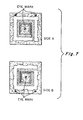
- the individual tag pattern is shown in Figure 7 where the final tag pattern is formed by aligning side A with side B such that the "x" and eye marks are registered on opposing surfaces of the film.
- Flexographic inks chosen to be resitant to the subsequent plating chemicals, serve as a plating mask to block off the non-circuit areas of the pretreated film. It is important to have close tolerance alignment ( ⁇ 38,1 . 10 -5 m ( ⁇ 15 mils) of the pattern from side-to-side, in order that the overlapping patterns form a distributive capacitor element as described in U.S. Patent Application Serial No. 565 350, filed December 27, 1983.
- the through-hole perforation on each tag is done at the same time as the printing at the exact area marked "x" in Figure 7, side A and side B.
- the film is further electroplated with copper.
- This can be accomplished in a typical vertical or horizontal reel-to-reel strip plating fashion where the film is passed through a series of electrolytic plating cells with constant voltage (progressively increasing amperage) causing copper to deposit on the conductive surface and build to a sufficient thickness to achieve desired resistance levels in the circuit patterns.
- copper was plated to a thickness of approximately 2,54 10 -5 m (1, 0 mil) over a period of 40 minutes through a series of 10 progressive electroplating cells with the bright acid copper bath described previously.
- the printed ink is stripped off in a 5 vol% butylcellosolve, 5% by weight sodium hydroxide aqueous solution at 45° - 50°C for 5 minutes in a continuous spray resist stripper.
- the film is rinsed and the thin electroless copper layer is etched from the non-circuit areas, previously protected by the ink, by an aqueous CuCl 2 solution at 45 0 - 50°C for 5 minutes in a continuous process.
- the copper was of sufficient thickness on each discrete circuit pattern from side A to side B to provide a resistance value of 0,2 ohms.
- Each individual circuit pattern has a dimension of 38,1 mm (1,5 inches) by 35,56 mm (1,4 inches). This process provided individual RF-tuned circuits with this particular pattern that had a frequency response of 8,2 MHz and a Q value of 60.
- the roll of repeating circuit tag patterns are then subsequently laminated with a cover paper on one side and a pressure sensitive adhesive with a removable protective backing paper on the other side; and slit and cut to form suitable product for individual tag application as an adhesive sticker label.
- the tags are cut into individual strips and rolled for easy dispensing from applicator devices. When separated from each other, the individual radio frequency-tuned circuit patterns function efficiently in a typical RF detector system used for electronic surveillance detection systems.
- the substrate film is advanced at a rate between about 10,16 . 10 m/s and 50,8 ⁇ 10 -3 m/s (2 and 10 feet/minute). Within this process rate range, the desired surface treatment is effected without mechanically damaging the film.
- a continuous strip of printed circuit patterns comprising a plurality of RF-tuned circuits was made by the following sequence of operations:
- the film is drawn through a bath containing 3 % turpentine in a water emulsion.
- the film is exposed to the platicizing solvent for a period of 5 minutes at a temperature of 65 - 70°C and then water rinsed to remove any excess solvent prior to immersion in the second treatment bath for 5 minutes which consists of 46° Baume chromic/sulfuric acid at 79,44°C (175 0 F) to effect surface etching of the film to enhance adhesion of the subsequent metal plating layer.
- the film is again water rinsed prior to immersion in a preconditioning bath of Macuplex 9320 which is at 50° - 55° C for a period of 5 minutes.
- Macuplex D-34 catalyst which is a colloidally dispersed palladium made from a combination of palladium and tin chlorides in 20% hydrochloric acid, at 20° - 25°C for a period of 5 minutes, and then finally rinsed, dried and rewound in a roll.
- the film is prepared for electroless copper deposition by first passing the film through an accelerator bath, Shipley Accelerator 19, a fluoroboric acid solution, for 3 - 4 minutes at 20° - 25°C which strips the tin from the catalytically activated film surface and exposes active palladium sites which initiate subsequent electroless copper deposition.
- the film is rinsed and then passed directly into an electroless copper bath, Hunt's Endura-plate EP 407, at 25°C for a period of 10 minutes which deposits approximately 38,1 . 10 -8 m to 50,8 ⁇ 10 -8 m (15 - 20 microinches) of electroless copper. This is sufficient to render the surface conductive for subsequent electrolytic copper plating.
- the film is then given a flash electroplate coating from an electroforming type bath (described previously) to a thickness of 177,8 - 10 -8 m to 203,2 ⁇ 10 -8 m (70 - 80 microinches).
- the metallized film is then printed with the positive image in a plurality of circuit patterns by a high-speed flexographic press at about 508 10 -3 m/s (100 feet per minute).
- the individual tag pattern is shown in Figure 8 where the final tag pattern is formed by aligning side A with side B such that the "x" and eye marks are registered on opposing surfaces of the film.
- Flexographic inks chosen to be resistant to the subsequent etching chemical, serve as a plating mask to block off the non-circuit areas of the pretreated film.
- the non-circuit areas are removed by etching in an aqueous CuCl 2 solution at 45° - 50°C for 5 minutes in a continuous process.
- the film is rinsed, and the ink stripped off in a 5 vol% butylcellosolve, 5% by weight sodium hydroxide aqueous solution at 45° - 50°C for 5 minutes using a continuous spray etcher.
- the film is electroplated with copper. This can be accomplished in a typical vertical or horizontal reel-to-reel strip plating fashion where the film is passed through a series of electrolytic plating cells with increasing amperage causing copper to deposit on the conductive surface and build to a sufficient thickness to achieve desired resistance levels in the circuit patterns.
- copper was plated to a thickness of approximately 2,54 - 10-5m (1 mil) over a period of 40 minutes through a series of 10 progressive electroplating cells.
- the copper was of sufficient thickness on each discrete circuit pattern from side 1 to side 2 to provide a resistance value of 0,2 ohms. This provided individual RF-tuned circuits with this particular pattern that had a frequency response of 8,2 MHz and a Q value of 70.
- Each circuit has a dimension of 50,8 mm (2 inches) by 50,8 mm (2 inches).
- the roll of repeating circuit tag patterns are then subsequently laminated with a cover paper on one side and a pressure sensitive adhesive with a removable protective backing paper on the other side; and slit and cut to form suitable product for individual tag application as an adhesive sticker label.
- the tags are cut into individual strips and rolled for easy dispensing from applicator devices. When separated from each other, the individual radio frequency-tuned circuit patterns function efficiently in a typical RF detector system used for electronic surveillance detection systems.
- the substrate film is advanced at a rate between about 10,16 ⁇ 10- 3 m/s and 50,8 - 10- 3 m/s (2 and 10 feet/minute). Within this process rate range, the desired surface treatment is effected without mechanically damaging the film.
- a continuous strip of printed circuit patterns comprising a plurality of RF-tuned circuits was made by the exact sequence described in Example II with the addition of printing a non-strippable ink over the conductive circuit wind as shown in Figure 9.
- This non-strippable ink, strip 90 was printed at the same time as the strippable ink and was printed over a thin layer of electroless copper. During subsequent plating steps, the copper under this ink does not plate, leaving a thin copper layer in the final plated circuit pattern. In the stripping operation, this non-strippable ink will not be removed, thus protecting the copper from being etched away in the copper etching solution.
- This thin copper layer, in the final tuned circuit will function as a fuse which can render the tag inoperative by means of radio frequency energy or contact with a high voltage source.
Landscapes
- Engineering & Computer Science (AREA)
- Manufacturing & Machinery (AREA)
- Microelectronics & Electronic Packaging (AREA)
- Chemical & Material Sciences (AREA)
- Chemical Kinetics & Catalysis (AREA)
- Electrochemistry (AREA)
- Materials Engineering (AREA)
- Metallurgy (AREA)
- Organic Chemistry (AREA)
- Chemically Coating (AREA)
- Laminated Bodies (AREA)
- Parts Printed On Printed Circuit Boards (AREA)
- Manufacturing Of Printed Wiring (AREA)
Applications Claiming Priority (2)
| Application Number | Priority Date | Filing Date | Title |
|---|---|---|---|
| US06/685,345 US4560445A (en) | 1984-12-24 | 1984-12-24 | Continuous process for fabricating metallic patterns on a thin film substrate |
| US685345 | 1984-12-24 |
Publications (2)
| Publication Number | Publication Date |
|---|---|
| EP0186185A2 true EP0186185A2 (de) | 1986-07-02 |
| EP0186185A3 EP0186185A3 (de) | 1988-10-05 |
Family
ID=24751790
Family Applications (1)
| Application Number | Title | Priority Date | Filing Date |
|---|---|---|---|
| EP85116495A Withdrawn EP0186185A3 (de) | 1984-12-24 | 1985-12-23 | Kontinuierliches Verfahren zur Herstellung metallischer Muster auf einem Dunnfilmsubstrat |
Country Status (4)
| Country | Link |
|---|---|
| US (1) | US4560445A (de) |
| EP (1) | EP0186185A3 (de) |
| JP (1) | JPS61203696A (de) |
| CA (1) | CA1277947C (de) |
Cited By (2)
| Publication number | Priority date | Publication date | Assignee | Title |
|---|---|---|---|---|
| EP0380426A1 (de) * | 1989-01-25 | 1990-08-01 | Tokai Electronics Co., Ltd. | Resonanzaufkleber sowie Verfahren zur Herstellung |
| US5201988A (en) * | 1989-01-25 | 1993-04-13 | Tokai Metals Co., Ltd. | Method of manufacturing a resonant tag |
Families Citing this family (76)
| Publication number | Priority date | Publication date | Assignee | Title |
|---|---|---|---|---|
| CH677988A5 (de) * | 1986-07-30 | 1991-07-15 | Actron Entwicklungs Ag | |
| US5325094A (en) * | 1986-11-25 | 1994-06-28 | Chomerics, Inc. | Electromagnetic energy absorbing structure |
| US5576710A (en) * | 1986-11-25 | 1996-11-19 | Chomerics, Inc. | Electromagnetic energy absorber |
| US5200068A (en) * | 1990-04-23 | 1993-04-06 | Andelman Marc D | Controlled charge chromatography system |
| US5415768A (en) * | 1990-04-23 | 1995-05-16 | Andelman; Marc D. | Flow-through capacitor |
| US5192432A (en) * | 1990-04-23 | 1993-03-09 | Andelman Marc D | Flow-through capacitor |
| US5196115A (en) * | 1990-04-23 | 1993-03-23 | Andelman Marc D | Controlled charge chromatography system |
| US5360540A (en) * | 1990-04-23 | 1994-11-01 | Andelman Marc D | Chromatography system |
| US6045652A (en) * | 1992-06-17 | 2000-04-04 | Micron Communications, Inc. | Method of manufacturing an enclosed transceiver |
| US7158031B2 (en) | 1992-08-12 | 2007-01-02 | Micron Technology, Inc. | Thin, flexible, RFID label and system for use |
| US5264288A (en) * | 1992-10-01 | 1993-11-23 | Ppg Industries, Inc. | Electroless process using silylated polyamine-noble metal complexes |
| US5381137A (en) * | 1992-10-26 | 1995-01-10 | Motorola, Inc. | RF tagging system and RF tags and method |
| US5336370A (en) * | 1993-12-09 | 1994-08-09 | Chipalkatti Makarand H | Pre-treatment for plating technique |
| US5444223A (en) | 1994-01-11 | 1995-08-22 | Blama; Michael J. | Radio frequency identification tag and method |
| US5751256A (en) * | 1994-03-04 | 1998-05-12 | Flexcon Company Inc. | Resonant tag labels and method of making same |
| US6309532B1 (en) | 1994-05-20 | 2001-10-30 | Regents Of The University Of California | Method and apparatus for capacitive deionization and electrochemical purification and regeneration of electrodes |
| US5545440A (en) * | 1994-12-05 | 1996-08-13 | At&T Global Information Solutions Company (Aka Ncr Corporation) | Method and apparatus for polymer coating of substrates |
| US5597469A (en) * | 1995-02-13 | 1997-01-28 | International Business Machines Corporation | Process for selective application of solder to circuit packages |
| US6466131B1 (en) * | 1996-07-30 | 2002-10-15 | Micron Technology, Inc. | Radio frequency data communications device with adjustable receiver sensitivity and method |
| FR2757315B1 (fr) * | 1996-12-17 | 1999-03-05 | Thomson Csf | Antenne reseau imprimee large bande |
| US6304169B1 (en) | 1997-01-02 | 2001-10-16 | C. W. Over Solutions, Inc. | Inductor-capacitor resonant circuits and improved methods of using same |
| DE19812812A1 (de) * | 1997-04-25 | 1999-09-23 | Whd Elektron Prueftech Gmbh | Aufbau von Sicherheitselementen für Dokumente und Vorrichtungen zur Prüfung von Dokumenten mit derartigen Sicherheitselementen sowie Verfahren zur Anwendung |
| US6339385B1 (en) * | 1997-08-20 | 2002-01-15 | Micron Technology, Inc. | Electronic communication devices, methods of forming electrical communication devices, and communication methods |
| US6143145A (en) * | 1997-10-02 | 2000-11-07 | Precious Plate Inc. | Apparatus for continuous masking for selective electroplating and method |
| US6331490B1 (en) * | 1998-03-13 | 2001-12-18 | Semitool, Inc. | Process for etching thin-film layers of a workpiece used to form microelectric circuits or components |
| US6632292B1 (en) | 1998-03-13 | 2003-10-14 | Semitool, Inc. | Selective treatment of microelectronic workpiece surfaces |
| JP3268386B2 (ja) * | 1998-06-29 | 2002-03-25 | 日本航空電子工業株式会社 | 腐食防止膜の形成方法 |
| US6346187B1 (en) | 1999-01-21 | 2002-02-12 | The Regents Of The University Of California | Alternating-polarity operation for complete regeneration of electrochemical deionization system |
| US8585852B2 (en) * | 1999-06-16 | 2013-11-19 | Vanguard Identification Systems, Inc. | Methods of making printed planar radio frequency identification elements |
| US6994262B1 (en) * | 1999-06-16 | 2006-02-07 | Vanguard Identification Systems, Inc. | Printed sheet products with integral, removable, radio frequency identification elements |
| US8636220B2 (en) | 2006-12-29 | 2014-01-28 | Vanguard Identification Systems, Inc. | Printed planar RFID element wristbands and like personal identification devices |
| US8654018B2 (en) * | 2005-04-06 | 2014-02-18 | Vanguard Identificaiton Systems, Inc. | Printed planar RFID element wristbands and like personal identification devices |
| US6240622B1 (en) * | 1999-07-09 | 2001-06-05 | Micron Technology, Inc. | Integrated circuit inductors |
| DE19940560C2 (de) * | 1999-08-26 | 2001-09-13 | Infineon Technologies Ag | Verfahren zur Herstellung eines Halbleiterchips mit nach dem Siliziumprozess einstellbarer elektrischer Eigenschaft |
| US6476775B1 (en) * | 2000-03-13 | 2002-11-05 | Rcd Technology Corporation | Method for forming radio frequency antenna |
| US6806812B1 (en) * | 2000-04-26 | 2004-10-19 | Micron Technology, Inc. | Automated antenna trim for transmitting and receiving semiconductor devices |
| WO2002080637A1 (en) | 2001-04-02 | 2002-10-10 | Nashua Corporation | Circuit elements having an embedded conductive trace and methods of manufacture |
| DE10121126A1 (de) * | 2001-04-30 | 2002-11-07 | Intec Holding Gmbh | Identifikationsträger und Verfahren zu dessen Herstellung |
| US6835412B2 (en) * | 2001-05-04 | 2004-12-28 | Micrometal Technologies, Inc. | Metalized dielectric substrates for EAS tags |
| DE10145749A1 (de) * | 2001-09-17 | 2003-04-24 | Infineon Technologies Ag | Verfahren zur Herstellung einer strukturierten Metallschicht auf einem Trägerkörper und Trägerkörper mit einer strukturierten Metallschicht |
| DE10145750A1 (de) * | 2001-09-17 | 2003-04-24 | Infineon Technologies Ag | Verfahren zur Herstellung einer Metallschicht auf einem Trägerkörper und Trägerkörper mit einer Metallschicht |
| US7113131B2 (en) * | 2002-05-02 | 2006-09-26 | Micrometal Technologies, Inc. | Metalized dielectric substrates for EAS tags |
| EP1383364A3 (de) * | 2002-05-23 | 2006-01-04 | Nashua Corporation | Schaltungselemente mit tintenaufnehmender Beschichtung und einer Leiterbahn und Verfahren zu deren Herstellung |
| US8465469B2 (en) * | 2002-09-12 | 2013-06-18 | Medtronic Vascular, Inc. | Reinforced catheter and methods of making |
| US7774035B2 (en) * | 2003-06-27 | 2010-08-10 | Superpower, Inc. | Superconducting articles having dual sided structures |
| US20040266628A1 (en) * | 2003-06-27 | 2004-12-30 | Superpower, Inc. | Novel superconducting articles, and methods for forming and using same |
| DE10342512B3 (de) * | 2003-09-12 | 2004-10-28 | Atotech Deutschland Gmbh | Vorrichtung und Verfahren zum elektrolytischen Behandeln von elektrisch gegeneinander isolierten, elektrisch leitfähigen Strukturen auf Oberflächen von bandförmigem Behandlungsgut |
| US7219627B1 (en) * | 2003-09-22 | 2007-05-22 | Electronic Materials Llc | Electrical bandage protector |
| US7755484B2 (en) * | 2004-02-12 | 2010-07-13 | Avery Dennison Corporation | RFID tag and method of manufacturing the same |
| US8099335B2 (en) * | 2004-02-23 | 2012-01-17 | Checkpoint Systems, Inc. | Method and system for determining billing information in a tag fabrication process |
| US7119685B2 (en) * | 2004-02-23 | 2006-10-10 | Checkpoint Systems, Inc. | Method for aligning capacitor plates in a security tag and a capacitor formed thereby |
| US7704346B2 (en) * | 2004-02-23 | 2010-04-27 | Checkpoint Systems, Inc. | Method of fabricating a security tag in an integrated surface processing system |
| US7116227B2 (en) * | 2004-02-23 | 2006-10-03 | Checkpoint Systems, Inc. | Tag having patterned circuit elements and a process for making same |
| US7138919B2 (en) * | 2004-02-23 | 2006-11-21 | Checkpoint Systems, Inc. | Identification marking and method for applying the identification marking to an item |
| US7384496B2 (en) | 2004-02-23 | 2008-06-10 | Checkpoint Systems, Inc. | Security tag system for fabricating a tag including an integrated surface processing system |
| US7255782B2 (en) * | 2004-04-30 | 2007-08-14 | Kenneth Crouse | Selective catalytic activation of non-conductive substrates |
| US20050241951A1 (en) * | 2004-04-30 | 2005-11-03 | Kenneth Crouse | Selective catalytic activation of non-conductive substrates |
| US7202790B2 (en) * | 2004-08-13 | 2007-04-10 | Sensormatic Electronics Corporation | Techniques for tuning an antenna to different operating frequencies |
| US7355516B2 (en) * | 2004-12-23 | 2008-04-08 | Checkpoint Systems, Inc. | Method and apparatus for protecting culinary products |
| DE102005006459A1 (de) * | 2005-02-12 | 2006-08-17 | Preh Gmbh | Metallisiertes Kunststoffbauteil mit einem Anzeigebereich und Verfahren zur Herstellung |
| US20060183342A1 (en) * | 2005-02-15 | 2006-08-17 | Eastman Kodak Company | Metal and metal oxide patterned device |
| US20070008059A1 (en) * | 2005-07-06 | 2007-01-11 | Triquint Semiconductor, Inc. | Misregistration-tolerant overlay inductors |
| JP2007219575A (ja) * | 2006-02-14 | 2007-08-30 | Checkpoint Manufacturing Japan Kk | 共振タグ |
| JP2008238681A (ja) * | 2007-03-28 | 2008-10-09 | Fujifilm Corp | ポリマーフィルムの延伸方法及び耳屑回収装置 |
| US7661307B1 (en) * | 2007-05-04 | 2010-02-16 | Milone Christopher J | Low manufacturing cost printed ink liquid level sensors |
| US8866616B2 (en) * | 2007-08-22 | 2014-10-21 | Tyco Fire & Security Gmbh | RFID tag having antenna with co-planar radiation pattern |
| US20090128417A1 (en) * | 2007-11-16 | 2009-05-21 | Rcd Technology, Inc. | Electroless/electrolytic seed layer process |
| US20100301006A1 (en) * | 2009-05-29 | 2010-12-02 | Nilsson Peter L J | Method of Manufacturing an Electrical Component on a Substrate |
| US20100301005A1 (en) * | 2009-05-29 | 2010-12-02 | Nilsson Peter L J | Method of Manufacturing an Electrical Circuit on a Substrate |
| US8716188B2 (en) | 2010-09-15 | 2014-05-06 | Superpower, Inc. | Structure to reduce electroplated stabilizer content |
| US9419502B2 (en) | 2012-08-03 | 2016-08-16 | Hamilton Sundstrand Corporation | Additive manufacturing of a component having a laminated stack of layers |
| JP6380028B2 (ja) * | 2014-11-13 | 2018-08-29 | 富士通株式会社 | インダクタの製造方法 |
| EP3350051B1 (de) | 2015-09-14 | 2022-08-03 | Neology, Inc. | Eingebettete borddiagnosevorrichtung für ein fahrzeug |
| DE202016008798U1 (de) * | 2015-10-08 | 2019-09-27 | Laird Technologies, Inc. | Selektiv plattierte Materialrollen |
| JP6776867B2 (ja) | 2016-12-15 | 2020-10-28 | Tdk株式会社 | 配線部品 |
| US20210249168A1 (en) * | 2020-02-11 | 2021-08-12 | Dupont Electronics, Inc. | Plated copper conductor structures for self-resonant sensor and manufacture thereof |
Family Cites Families (9)
| Publication number | Priority date | Publication date | Assignee | Title |
|---|---|---|---|---|
| US3167490A (en) * | 1957-07-17 | 1965-01-26 | Friedman Abraham | Printed circuit |
| US3208921A (en) * | 1962-01-02 | 1965-09-28 | Sperry Rand Corp | Method for making printed circuit boards |
| US3666549A (en) * | 1969-05-09 | 1972-05-30 | Macdermid Inc | Method of making additive printed circuit boards and product thereof |
| US3810147A (en) * | 1971-12-30 | 1974-05-07 | G Lichtblau | Electronic security system |
| US4082618A (en) * | 1974-07-31 | 1978-04-04 | Daiichi Denshi Kogyo Kabushiki Kaisha | Method for electrolytic treatment |
| US3956077A (en) * | 1975-03-27 | 1976-05-11 | Western Electric Company, Inc. | Methods of providing contact between two members normally separable by an intervening member |
| US4261800A (en) * | 1977-08-15 | 1981-04-14 | Western Electric Co., Inc. | Method of selectively depositing a metal on a surface of a substrate |
| DE2757029A1 (de) * | 1977-12-21 | 1980-01-31 | Guenther Dr Ing Herrmann | Verfahren zur herstellung einer schaltungsplatte |
| US4217182A (en) * | 1978-06-07 | 1980-08-12 | Litton Systems, Inc. | Semi-additive process of manufacturing a printed circuit |
-
1984
- 1984-12-24 US US06/685,345 patent/US4560445A/en not_active Expired - Fee Related
-
1985
- 1985-12-13 CA CA000497598A patent/CA1277947C/en not_active Expired - Fee Related
- 1985-12-23 EP EP85116495A patent/EP0186185A3/de not_active Withdrawn
- 1985-12-23 JP JP60290302A patent/JPS61203696A/ja active Pending
Cited By (3)
| Publication number | Priority date | Publication date | Assignee | Title |
|---|---|---|---|---|
| EP0380426A1 (de) * | 1989-01-25 | 1990-08-01 | Tokai Electronics Co., Ltd. | Resonanzaufkleber sowie Verfahren zur Herstellung |
| US5119070A (en) * | 1989-01-25 | 1992-06-02 | Tokai Metals Co., Ltd. | Resonant tag |
| US5201988A (en) * | 1989-01-25 | 1993-04-13 | Tokai Metals Co., Ltd. | Method of manufacturing a resonant tag |
Also Published As
| Publication number | Publication date |
|---|---|
| EP0186185A3 (de) | 1988-10-05 |
| CA1277947C (en) | 1990-12-18 |
| JPS61203696A (ja) | 1986-09-09 |
| US4560445A (en) | 1985-12-24 |
Similar Documents
| Publication | Publication Date | Title |
|---|---|---|
| US4560445A (en) | Continuous process for fabricating metallic patterns on a thin film substrate | |
| US4555414A (en) | Process for producing composite product having patterned metal layer | |
| US4666735A (en) | Process for producing product having patterned metal layer | |
| US7578048B2 (en) | Patterns of conductive objects on a substrate coated with inorganic compounds and method of producing thereof | |
| US20090165296A1 (en) | Patterns of conductive objects on a substrate and method of producing thereof | |
| EP0380545B1 (de) | SCHALTUNGSPLATTENMATERIAL UND ELEKTROPLATTIERUNGSBAD FüR SEINE HERSTELLUNG | |
| JP2595151B2 (ja) | 耐積層剥離性の金属フィルム積層板 | |
| US5374454A (en) | Method for conditioning halogenated polymeric materials and structures fabricated therewith | |
| US3625758A (en) | Base material and method for the manufacture of printed circuits | |
| US3936548A (en) | Method for the production of material for printed circuits and material for printed circuits | |
| US4869930A (en) | Method for preparing substrates for deposition of metal seed from an organometallic vapor for subsequent electroless metallization | |
| JPH0383395A (ja) | 印刷回路基板の製造方法 | |
| GB1565039A (en) | Boards for use in printed circuits and their manufacture | |
| JP2004510061A (ja) | 誘電体を選択的に金属化する方法 | |
| US20090293268A1 (en) | Patterns of conductive objects on a substrate and method of producing thereof | |
| KR100649783B1 (ko) | 도전층의 밀착성을 향상시킨 도전성 시트 | |
| EP0153683B1 (de) | Verfahren zur Herstellung von Leiterplatten | |
| EP0257737A2 (de) | Gedruckte Schaltungsvorläufer | |
| CA2203171A1 (en) | Process for coating electrically non-conducting surfaces with connected metal structures | |
| US20040076743A1 (en) | Method for the manufacture of printed circuit boards with integral plated resistors | |
| US7683785B2 (en) | RF tags | |
| KR101603967B1 (ko) | 연속 패턴 도금 전사 시스템 및 연속 패턴 도금 전사물 제조 방법 | |
| US4486273A (en) | Selective plating of dielectric substrates | |
| EP0298345A2 (de) | Verfahren zur Herstellung von Substraten für nachträgliche stromlose Metallisierung | |
| US6120672A (en) | Process for manufacturing inductive counting systems |
Legal Events
| Date | Code | Title | Description |
|---|---|---|---|
| PUAI | Public reference made under article 153(3) epc to a published international application that has entered the european phase |
Free format text: ORIGINAL CODE: 0009012 |
|
| AK | Designated contracting states |
Kind code of ref document: A2 Designated state(s): AT BE CH DE FR GB IT LI LU NL SE |
|
| PUAL | Search report despatched |
Free format text: ORIGINAL CODE: 0009013 |
|
| AK | Designated contracting states |
Kind code of ref document: A3 Designated state(s): AT BE CH DE FR GB IT LI LU NL SE |
|
| 17P | Request for examination filed |
Effective date: 19890329 |
|
| 17Q | First examination report despatched |
Effective date: 19891207 |
|
| STAA | Information on the status of an ep patent application or granted ep patent |
Free format text: STATUS: THE APPLICATION IS DEEMED TO BE WITHDRAWN |
|
| 18D | Application deemed to be withdrawn |
Effective date: 19910703 |
|
| RIN1 | Information on inventor provided before grant (corrected) |
Inventor name: VANDEBULT, JAN Inventor name: REILLY, PHILLIP B. Inventor name: HOOVER, MERVIN F. Inventor name: SALAMONE, ANN B. |