EP0186740A1 - Système de détection de la fréquence du secteur - Google Patents
Système de détection de la fréquence du secteur Download PDFInfo
- Publication number
- EP0186740A1 EP0186740A1 EP85112813A EP85112813A EP0186740A1 EP 0186740 A1 EP0186740 A1 EP 0186740A1 EP 85112813 A EP85112813 A EP 85112813A EP 85112813 A EP85112813 A EP 85112813A EP 0186740 A1 EP0186740 A1 EP 0186740A1
- Authority
- EP
- European Patent Office
- Prior art keywords
- detection
- zero
- signal
- cross
- output
- Prior art date
- Legal status (The legal status is an assumption and is not a legal conclusion. Google has not performed a legal analysis and makes no representation as to the accuracy of the status listed.)
- Granted
Links
Images


Classifications
-
- G—PHYSICS
- G01—MEASURING; TESTING
- G01R—MEASURING ELECTRIC VARIABLES; MEASURING MAGNETIC VARIABLES
- G01R19/00—Arrangements for measuring currents or voltages or for indicating presence or sign thereof
- G01R19/175—Indicating the instants of passage of current or voltage through a given value, e.g. passage through zero
-
- G—PHYSICS
- G01—MEASURING; TESTING
- G01R—MEASURING ELECTRIC VARIABLES; MEASURING MAGNETIC VARIABLES
- G01R23/00—Arrangements for measuring frequencies; Arrangements for analysing frequency spectra
- G01R23/02—Arrangements for measuring frequency, e.g. pulse repetition rate; Arrangements for measuring period of current or voltage
Definitions
- the present invention relates to a detection system for detecting a frequency of a power supply voltage and, more particularly, to a power frequency detection circuit in a signal transmission system which utilizes the building or house wiring.
- a signal transmission system has been developed, which utilizes the building or house wiring as a data transmission line.
- the power frequency is often used as a reference clock. To achieve an accurate operation, the power frequency component must be correctly detected without regard to the noises.
- an object of the present invention is to provide a detection system for detecting a frequency component of a power voltage.
- Another object of the present invention is to provide a power frequency detection system for use in a signal transmission system which utilizes the building or house wiring as a data transmission line.
- a zero-cross level detection circuit for detecting the frequency component of the power voltage applied thereto.
- An inhibition system is provided for precluding the operation of the zero-cross level detection circuit for a preselected period of time after the zero-cross level detection circuit has developed the last detection output. The inhibition system minimizes an erroneous operation of the zero-cross level detection circuit, that is, the zero-cross level detection circuit will not recognize the noises as the power frequency component as long as the noises are introduced into the system while the zero-cross level detection circuit is placed in an inoperative condition by the inhibition system.
- FIGURE 1 shows a typical construction of the zero-cross level detection circuit which includes a transistor 10 and a diode 12.
- a system timing signal is obtained through the use of the leading edge or the trailing edge of a synchronization output derived from the zero-cross level detection circuit (see FIGURE 2).
- the frequency of the occurrence of the erroneous detection output 14 is considerably lower than the power frequency. Furthermore, the power frequency is normally known. Therefore, if a system is constructed to neglect the power voltage variation for a preselected period of time after the last edge has been detected, the erroneous detection output 1 4 will be removed.
- FIGURE 3 shows an embodiment of a power frequency detection system of the present invention.
- FIGURE 4 shows another embodiment of the power frequency detection system of the present invention.
- Two embodiments differ from each other at an edge detection section for detecting the zero-cross timing of the power supply voltage. Both embodiments include a monomultivibrator 20 (not re- triggerable).
- the monomuttivibrator 20 must be triggered by edges of a same polarity every half cycle of the power supply voltage.
- a detection output of a zero-cross level detection circuit which includes the transistor 10 and the diode 12, is directly applied to one input terminal of an exclusive OR gate 22.
- the other input terminal of the exclusive OR gate 22 receives a delayed detection output of the zero-cross detection circuit via an integration circuit including a resistor 24 and a capacitor 26.
- An output signal of the exclusive OR gate 22 is applied to the monomultivibrator 20.
- a zero-cross level detection circuit includes photo-couplers 30 and 32 which function, in combination, as a wired OR gate.
- a point 34 provides a detection output signal as shown in FIGURE 5.
- the thus obtained detection output signal is applied to the monomuttivibrator 20.
- the output signal of the exclusive OR gate 22 in FIGURE 3 or the output signal obtained at the point 34 in FIGURE 4 bears a high level when the power voltage polarity changes. That is, the output signals of the exclusive OR gate 22 and the photo-couplers 30 and 32 are the zero-cross detection signal.
- noises such as an erroneous detection signal 36 are neglected as long as the monomultivibrator 20 is in the set state. That is, an output signal of the monomuttivibrator 20 is not influenced by the erroneous detection signal 36.
- the pulse width of the monomuttivibrator 20 is selected slightly shorter than one half of the period of the power supply voltage.
- the pulse width of the monomultivibrator 20 is selected at 7.5 milliseconds when the power supply voltage has a frequency of 60 Hz.
- a microcomputer is widely used in a control system of the power line signal transmission system.
- the microcomputer includes a programmable timer. By utilizing the programmable timer, a desired operation can be conducted as the circuits shown in FIGURES 3 and 4.
- FIGURE 6 shows an operational flow when the above- mentioned programmable timer is used to control the power frequency detection.
- the programmable timer is set to a desired value. Then, the data processing is conducted. After the preselected period of time has passed, the above- mentioned edge detection is carried out When the edge is detected, the programmable timer is again set to perform the next edge detection.
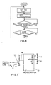
- a one-chip microcomputer 40 generally includes an input/ output port of the suspected bidirectional type. One of the bits can be used to form an analog integration timer as shown in FIGURE 7. More specifically, a resistor 42 and a capacitor 44 are connected to a terminal 46 of the microcomputer 40. The zero-cross level detection circuit including the transistor 10 and diode 12 is connected to a terminal 48 of the microcomputer 40.
- FIGURE 8 shows signals occurring within the circuit of FIGURE 7.
- FIGURE 9 shows an operational flow of the circuit of FIGURE 7.
- the input/output bit is set to "1". Then, the data processing operation is conducted. Thereafter, a determination is conducted as to whether the introduced input/output bit (signal at the terminal 46) is "1". If an affirmative answer is obtained, the input/output bit is set to "0", and the edge detection operation is carried out
- V th is about 1.4 volts
- V s is 5 votts.
- k is 0.33.
- the one half period is 8.3 milliseconds.
- the capacitance value C of the capacitor 44 should be selected between 6.9 microfarads and 6.8 microfarads because the resistor 42 is generally selected at 3.3 kiloohms due to the sink current in the input/ output port (generally, 1.6 milliamperes).
Landscapes
- Physics & Mathematics (AREA)
- General Physics & Mathematics (AREA)
- Measurement Of Current Or Voltage (AREA)
- Measuring Frequencies, Analyzing Spectra (AREA)
Priority Applications (2)
| Application Number | Priority Date | Filing Date | Title |
|---|---|---|---|
| EP19850112813 EP0186740B1 (fr) | 1982-12-30 | 1982-12-30 | Système de détection de la fréquence du secteur |
| DE8585112813T DE3280239D1 (de) | 1982-12-30 | 1982-12-30 | Netzfrequenzdetektorsystem. |
Applications Claiming Priority (1)
| Application Number | Priority Date | Filing Date | Title |
|---|---|---|---|
| EP19850112813 EP0186740B1 (fr) | 1982-12-30 | 1982-12-30 | Système de détection de la fréquence du secteur |
Related Parent Applications (2)
| Application Number | Title | Priority Date | Filing Date |
|---|---|---|---|
| EP19820307005 Division-Into EP0112948B1 (fr) | 1982-12-30 | 1982-12-30 | Système de détection de la fréquence du secteur |
| EP19820307005 Division EP0112948B1 (fr) | 1982-12-30 | 1982-12-30 | Système de détection de la fréquence du secteur |
Publications (2)
| Publication Number | Publication Date |
|---|---|
| EP0186740A1 true EP0186740A1 (fr) | 1986-07-09 |
| EP0186740B1 EP0186740B1 (fr) | 1990-09-05 |
Family
ID=8193814
Family Applications (1)
| Application Number | Title | Priority Date | Filing Date |
|---|---|---|---|
| EP19850112813 Expired EP0186740B1 (fr) | 1982-12-30 | 1982-12-30 | Système de détection de la fréquence du secteur |
Country Status (2)
| Country | Link |
|---|---|
| EP (1) | EP0186740B1 (fr) |
| DE (1) | DE3280239D1 (fr) |
Cited By (2)
| Publication number | Priority date | Publication date | Assignee | Title |
|---|---|---|---|---|
| GB2200006A (en) * | 1986-12-19 | 1988-07-20 | Lytemode Limited | Phase-controlled thyristor circuit |
| CN111366778A (zh) * | 2018-12-25 | 2020-07-03 | 施耐德电气(澳大利亚)有限公司 | 用于检测电信号的过零时刻的方法和设备、电子调节设备 |
Citations (2)
| Publication number | Priority date | Publication date | Assignee | Title |
|---|---|---|---|---|
| DE2713945B1 (de) * | 1977-03-29 | 1978-01-05 | Siemens Ag | Schaltungsanordnung zur ermittlung der impulsabstaende und/oder folgefrequenz von impulsen einer impulsfolge |
| EP0112948A1 (fr) * | 1982-12-30 | 1984-07-11 | Sharp Kabushiki Kaisha | Système de détection de la fréquence du secteur |
-
1982
- 1982-12-30 DE DE8585112813T patent/DE3280239D1/de not_active Expired - Lifetime
- 1982-12-30 EP EP19850112813 patent/EP0186740B1/fr not_active Expired
Patent Citations (2)
| Publication number | Priority date | Publication date | Assignee | Title |
|---|---|---|---|---|
| DE2713945B1 (de) * | 1977-03-29 | 1978-01-05 | Siemens Ag | Schaltungsanordnung zur ermittlung der impulsabstaende und/oder folgefrequenz von impulsen einer impulsfolge |
| EP0112948A1 (fr) * | 1982-12-30 | 1984-07-11 | Sharp Kabushiki Kaisha | Système de détection de la fréquence du secteur |
Non-Patent Citations (2)
| Title |
|---|
| IBM TECHNICAL DISCLOSURE BULLETIN, vol. 24, no. 10, March 1982, pages 5025-5027, New York, US; J.H. DODGE et al.: "Microcomputer control of zero-corssing detection accuracy" * |
| PATENTS ABSTRACTS OF JAPAN, vol. 6, no. 141 (P-131)[1019], 30th July 1982; & JP - A - 57 64 170 (TEAC K.K.) 19-04-1982 * |
Cited By (3)
| Publication number | Priority date | Publication date | Assignee | Title |
|---|---|---|---|---|
| GB2200006A (en) * | 1986-12-19 | 1988-07-20 | Lytemode Limited | Phase-controlled thyristor circuit |
| CN111366778A (zh) * | 2018-12-25 | 2020-07-03 | 施耐德电气(澳大利亚)有限公司 | 用于检测电信号的过零时刻的方法和设备、电子调节设备 |
| CN111366778B (zh) * | 2018-12-25 | 2022-12-27 | 施耐德电气(澳大利亚)有限公司 | 用于检测电信号的过零时刻的方法和设备、电子调节设备 |
Also Published As
| Publication number | Publication date |
|---|---|
| EP0186740B1 (fr) | 1990-09-05 |
| DE3280239D1 (de) | 1990-10-11 |
Similar Documents
| Publication | Publication Date | Title |
|---|---|---|
| US4412327A (en) | Test circuit for checking memory output state continuously during time window | |
| GB2032666A (en) | Multi-zone alarm system | |
| KR960005555A (ko) | 위상비교회로 및 피엘엘(pll)회로 | |
| US4622478A (en) | Power frequency detection system | |
| EP0186740A1 (fr) | Système de détection de la fréquence du secteur | |
| EP0112948A1 (fr) | Système de détection de la fréquence du secteur | |
| KR930701024A (ko) | 신호 존재 또는 부재의 선택적 검출장치 및 방법 | |
| US4853685A (en) | Switch monitoring arrangement with remote adjustment capability having debounce circuitry for accurate state determination | |
| US4852104A (en) | Solid-state reader device for a cumulative operations measurement system | |
| CA1198476A (fr) | Systeme de detection de frequence d'alimentation | |
| KR890001272A (ko) | 신호 판별회로 | |
| US5966034A (en) | Method and device for the filtering of a pulse signal | |
| EP0110893B1 (fr) | Procede et dispositif de detection de variations de frequences | |
| JPH0133052B2 (fr) | ||
| RU2143727C1 (ru) | Устройство для контроля функционирования блока обработки данных | |
| SU935832A1 (ru) | Устройство дл контрол сопротивлени изол ции | |
| JP2984175B2 (ja) | 火災感知器 | |
| SU1707752A1 (ru) | Селектор импульсов | |
| US6459752B1 (en) | Configuration and method for determining whether the counter reading of a counter has reached a predetermined value or not | |
| SU1647551A1 (ru) | Емкостное устройство дл ввода данных | |
| JPH0556480A (ja) | 検波装置 | |
| SU1601607A1 (ru) | Устройство дл селекции сигналов поверки времени | |
| RU2024906C1 (ru) | Устройство для допускового контроля временных интервалов | |
| JPS6115437A (ja) | シリアルデ−タ受信系のスタ−トビツト検出回路 | |
| SU1293761A1 (ru) | Устройство дл контрол блоков буферной пам ти |
Legal Events
| Date | Code | Title | Description |
|---|---|---|---|
| PUAI | Public reference made under article 153(3) epc to a published international application that has entered the european phase |
Free format text: ORIGINAL CODE: 0009012 |
|
| AC | Divisional application: reference to earlier application |
Ref document number: 112948 Country of ref document: EP |
|
| AK | Designated contracting states |
Kind code of ref document: A1 Designated state(s): DE FR GB IT |
|
| 17P | Request for examination filed |
Effective date: 19860929 |
|
| 17Q | First examination report despatched |
Effective date: 19890310 |
|
| ITF | It: translation for a ep patent filed | ||
| GRAA | (expected) grant |
Free format text: ORIGINAL CODE: 0009210 |
|
| AC | Divisional application: reference to earlier application |
Ref document number: 112948 Country of ref document: EP |
|
| AK | Designated contracting states |
Kind code of ref document: B1 Designated state(s): DE FR GB IT |
|
| REF | Corresponds to: |
Ref document number: 3280239 Country of ref document: DE Date of ref document: 19901011 |
|
| ET | Fr: translation filed | ||
| ITTA | It: last paid annual fee | ||
| PLBE | No opposition filed within time limit |
Free format text: ORIGINAL CODE: 0009261 |
|
| STAA | Information on the status of an ep patent application or granted ep patent |
Free format text: STATUS: NO OPPOSITION FILED WITHIN TIME LIMIT |
|
| 26N | No opposition filed | ||
| PGFP | Annual fee paid to national office [announced via postgrant information from national office to epo] |
Ref country code: FR Payment date: 19961211 Year of fee payment: 15 |
|
| PGFP | Annual fee paid to national office [announced via postgrant information from national office to epo] |
Ref country code: GB Payment date: 19961223 Year of fee payment: 15 |
|
| PGFP | Annual fee paid to national office [announced via postgrant information from national office to epo] |
Ref country code: DE Payment date: 19970107 Year of fee payment: 15 |
|
| PG25 | Lapsed in a contracting state [announced via postgrant information from national office to epo] |
Ref country code: GB Free format text: LAPSE BECAUSE OF NON-PAYMENT OF DUE FEES Effective date: 19971230 |
|
| PG25 | Lapsed in a contracting state [announced via postgrant information from national office to epo] |
Ref country code: FR Free format text: THE PATENT HAS BEEN ANNULLED BY A DECISION OF A NATIONAL AUTHORITY Effective date: 19971231 |
|
| GBPC | Gb: european patent ceased through non-payment of renewal fee |
Effective date: 19971230 |
|
| PG25 | Lapsed in a contracting state [announced via postgrant information from national office to epo] |
Ref country code: DE Free format text: LAPSE BECAUSE OF NON-PAYMENT OF DUE FEES Effective date: 19980901 |
|
| REG | Reference to a national code |
Ref country code: FR Ref legal event code: ST |