EP0186773B1 - Schutzschaltung für eine Kippschaltung gegen Fehler des "Soft error"-Typs - Google Patents
Schutzschaltung für eine Kippschaltung gegen Fehler des "Soft error"-Typs Download PDFInfo
- Publication number
- EP0186773B1 EP0186773B1 EP85114818A EP85114818A EP0186773B1 EP 0186773 B1 EP0186773 B1 EP 0186773B1 EP 85114818 A EP85114818 A EP 85114818A EP 85114818 A EP85114818 A EP 85114818A EP 0186773 B1 EP0186773 B1 EP 0186773B1
- Authority
- EP
- European Patent Office
- Prior art keywords
- node
- write
- capacitor
- latch
- field effect
- Prior art date
- Legal status (The legal status is an assumption and is not a legal conclusion. Google has not performed a legal analysis and makes no representation as to the accuracy of the status listed.)
- Expired
Links
- 230000004224 protection Effects 0.000 title claims description 11
- 239000003990 capacitor Substances 0.000 claims description 76
- 230000005669 field effect Effects 0.000 claims description 39
- 238000009792 diffusion process Methods 0.000 claims description 37
- 230000002708 enhancing effect Effects 0.000 claims description 15
- 210000000352 storage cell Anatomy 0.000 claims description 10
- 239000000758 substrate Substances 0.000 description 14
- JJWKPURADFRFRB-UHFFFAOYSA-N carbonyl sulfide Chemical compound O=C=S JJWKPURADFRFRB-UHFFFAOYSA-N 0.000 description 12
- 238000012360 testing method Methods 0.000 description 6
- 238000010586 diagram Methods 0.000 description 5
- 230000000295 complement effect Effects 0.000 description 3
- 239000012212 insulator Substances 0.000 description 3
- XUIMIQQOPSSXEZ-UHFFFAOYSA-N Silicon Chemical compound [Si] XUIMIQQOPSSXEZ-UHFFFAOYSA-N 0.000 description 2
- 238000006880 cross-coupling reaction Methods 0.000 description 2
- 230000000694 effects Effects 0.000 description 2
- 239000000463 material Substances 0.000 description 2
- 230000001681 protective effect Effects 0.000 description 2
- 229910052710 silicon Inorganic materials 0.000 description 2
- 239000010703 silicon Substances 0.000 description 2
- 239000002800 charge carrier Substances 0.000 description 1
- 238000007599 discharging Methods 0.000 description 1
- 239000002019 doping agent Substances 0.000 description 1
- 230000005684 electric field Effects 0.000 description 1
- 238000005516 engineering process Methods 0.000 description 1
- 239000012634 fragment Substances 0.000 description 1
- 230000006870 function Effects 0.000 description 1
- 230000005865 ionizing radiation Effects 0.000 description 1
- 230000000149 penetrating effect Effects 0.000 description 1
- 230000009993 protective function Effects 0.000 description 1
- 230000005855 radiation Effects 0.000 description 1
- 238000011084 recovery Methods 0.000 description 1
- 230000002787 reinforcement Effects 0.000 description 1
- 239000004065 semiconductor Substances 0.000 description 1
Images


Classifications
-
- H—ELECTRICITY
- H03—ELECTRONIC CIRCUITRY
- H03K—PULSE TECHNIQUE
- H03K3/00—Circuits for generating electric pulses; Monostable, bistable or multistable circuits
- H03K3/02—Generators characterised by the type of circuit or by the means used for producing pulses
- H03K3/353—Generators characterised by the type of circuit or by the means used for producing pulses by the use, as active elements, of field-effect transistors with internal or external positive feedback
- H03K3/356—Bistable circuits
- H03K3/356086—Bistable circuits with additional means for controlling the main nodes
-
- G—PHYSICS
- G11—INFORMATION STORAGE
- G11C—STATIC STORES
- G11C11/00—Digital stores characterised by the use of particular electric or magnetic storage elements; Storage elements therefor
- G11C11/21—Digital stores characterised by the use of particular electric or magnetic storage elements; Storage elements therefor using electric elements
- G11C11/34—Digital stores characterised by the use of particular electric or magnetic storage elements; Storage elements therefor using electric elements using semiconductor devices
- G11C11/40—Digital stores characterised by the use of particular electric or magnetic storage elements; Storage elements therefor using electric elements using semiconductor devices using transistors
- G11C11/401—Digital stores characterised by the use of particular electric or magnetic storage elements; Storage elements therefor using electric elements using semiconductor devices using transistors forming cells needing refreshing or charge regeneration, i.e. dynamic cells
- G11C11/4063—Auxiliary circuits, e.g. for addressing, decoding, driving, writing, sensing or timing
- G11C11/407—Auxiliary circuits, e.g. for addressing, decoding, driving, writing, sensing or timing for memory cells of the field-effect type
- G11C11/409—Read-write [R-W] circuits
- G11C11/4094—Bit-line management or control circuits
-
- G—PHYSICS
- G11—INFORMATION STORAGE
- G11C—STATIC STORES
- G11C7/00—Arrangements for writing information into, or reading information out from, a digital store
- G11C7/12—Bit line control circuits, e.g. drivers, boosters, pull-up circuits, pull-down circuits, precharging circuits, equalising circuits, for bit lines
-
- H—ELECTRICITY
- H03—ELECTRONIC CIRCUITRY
- H03K—PULSE TECHNIQUE
- H03K3/00—Circuits for generating electric pulses; Monostable, bistable or multistable circuits
- H03K3/02—Generators characterised by the type of circuit or by the means used for producing pulses
- H03K3/027—Generators characterised by the type of circuit or by the means used for producing pulses by the use of logic circuits, with internal or external positive feedback
- H03K3/037—Bistable circuits
- H03K3/0375—Bistable circuits provided with means for increasing reliability; for protection; for ensuring a predetermined initial state when the supply voltage has been applied; for storing the actual state when the supply voltage fails
Definitions
- the invention disclosed herein broadly relates to transistor circuits and more particularly relates to protective circuits for preserving the stored binary state of a transistor circuit storage device or latch.
- VLSI very large scale integrated
- the N channel field effect transistor circuit technology will be the example used herein.
- the abbreviation NFET will be used herein to refer to an N channel field effect transistor device.
- Such devices are generally fabricated by forming an N-type conductivity source diffusion and N-type diffusion in the surface of a P-type conductivity silicon substrate. The channel region of the substrate separating the source and drain regions, is covered by a gate insulator layer and a gate electrode.
- An enhancement mode NFET is normally nonconducting between its source and drain and it can be switched into conduction by applying a positive potential to its gate electrode, with respect to the potential of its source.
- a depletion mode NFET is normally conducting between its source and drain and it can be switched into nonconduction by applying a negative potential to its gate electrode, with respect to the potential of its source.
- a typical NFET integrated circuit latch 6 is shown in a portion of Figure 1.
- the latch 6 is a level sensitive scan design (LSSD) latch which stores one binary bit of information, and can be used either to store a test bit during test operations or it can store a data bit during normal logic function operations.
- the latch 6 consists of a pair of cross-coupled inverters.
- the first inverter is composed of the NFET enhancement mode active device 50 and the NFET depletion mode load device 52 which are series-connected between the drain potential Vdd at 10 of approximately five volts and ground potential. The convention is adopted that the drain potential of Vdd represents a binary logic value of "1" and ground potential represents a binary logic value of "0.”
- the binary "1" potential of Vdd exists at the output node 8 ⁇ and the load device 52 is no longer conducting current. Since the gate electrode is connected to the source for the load device 52, it is never negatively biased with respect to the source and therefore the load device is always capable of supplying current to the node 8 ⁇ whenever the potential of the node 8 ⁇ is less than the drain potential Vdd.
- the latch 6 is made up of two inverters, the first inverter being devices 50 and 52 and the second inverter being devices 70 and 72.
- the second inverter is identical to the first inverter, devices 50 and 70 being both NFET enhancement mode devices and devices 52 and 72 being both NFET depletion mode devices.
- the latch 6 when the first node 8 ⁇ is at a higher potential than the second node 8, the latch 6 will be storing a binary "1" value and when the first node 8 ⁇ is at a lower potential than the second node 8, the latch 6 will be storing a binary "0" value.
- the state of the binary bit stored in the latch 6 can be read by sensing the relative potential of the first node 8 ⁇ with respect to the second node 8, or by sensing the individual nodes 8 or 8 ⁇ , exclusively.
- a first data input circuit is connected to the first node 8 ⁇ consisting of the series-connected NFET enhancement mode devices 12 and 16 and a second data input circuit is connected to the second node 8 consisting of the series-connected NFET enhancement mode devices 12 ⁇ and 16 ⁇ .
- the gates of devices 16 and 16 ⁇ are connected to a write-enable (WE) input 14 which, when on, defines the write intervals when the state of the latch 6 can be changed.
- WE write-enable
- the write-enable signal is also known as the "C-clock.” If the DATA* input 15 to the gate of device 12 is on while the WE input 14 to the gate of device 16 is on, then the first node 8 ⁇ is connected to ground potential and the latch 6 has its binary storage state changed to the "0" state.
- the latch 6 also has test inputs to accept LSSD scan string test bits then circuit testing is desired.
- a first scan input circuit is connected to the first node 8 ⁇ consisting of the series-connected NFET enhancement mode devices 76 and 74 and a second scan input circuit is connected to the second node 8 consisting of the series-connected NFET enhancement mode devices 76 ⁇ and 74 ⁇ .
- the gates of devices 74 and 74 ⁇ are connected to the A-clock (A-CLK) input which, when on, defines the scan-write intervals when the state of the latch 6 can be changed.
- the SCAN* input to the gate of device 76 is on while the A-CLK input to the gate of device 74 is on, then the first node 8 ⁇ is connected to ground potential and the latch 6 has its binary storage state changed to the "0" state. Alternately, if the SCAN input to the gate of device 76 ⁇ is on while the A-CLK input to the gate of device 74 ⁇ is on, then the second node 8 is connected to ground potential and the latch 6 has its binary storage state changed to the "1" state.
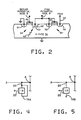
- the effect of an electrostatic perturbation, such as a cosmic ray, on the binary storage state of a latch can be better understood by examining the cross-sectional view of the structure of the first inverter in the latch 6, as is depicted in Figure 2.
- the NFET enhancement mode active device 50 and the NFET depletion mode load device 52 are shown in Figure 2 as being formed in the P-type silicon substrate 54.
- the load device 52 has its N-type drain 56 and its N-type source 58 formed in the P-type substrate 54, and the gate insulator and the gate electrode 60 formed over the channel region separating the source 58 and drain 56.
- the load device 52 is made a depletion mode by ion implanting an N-type dopant in the channel region thereof.
- the drain 56 is connected to the positive drain potential Vdd.
- the source 58 and the gate 60 are connected in common to the latch node 8 ⁇ .
- the substrate 54 is connected to ground potential and therefore the source 58 and the drain 56, which are both N-type, form a reversed bias junction with the P-type substrate 54.
- the active device 50 has its N-type drain 62 and its N-type source 64 formed in the P-type substrate 54, and the gate insulator and the gate electrode 66 formed over the channel region separating the source 64 and drain 62.
- the drain 62 is connected to the latch node 8 ⁇ and the source 64 is connected to ground potential.
- the first inverter has its output node 8 ⁇ at the positive Vdd potential and the gate electrode 66 of the active device 50 is at ground potential, keeping the active device 50 nonconducting.
- the positive potential of the N-type drain diffusion 62 with respect to the ground potential of the substrate 54 creates a reversed bias PN junction 63 between the drain 62 and the substrate 54.
- the reversed bias PN junction 63 forms a region which is depleted of charge carriers, bounded by a layer of electrons on the N-type side and by a layer of positive charges on the P-type side. This creates an electric field in the depleted region of junction 63 which will sweep out any free charges which may occur therein, causing a small current. If the electrostatically charged track of a cosmic ray 68 passes within the vicinity of the reversed bias PN junction 63, the charges liberated in the depletion region of the junction 63 are swept out, causing a current spike of up to 30 milliamperes for a duration of from 0.1 to 0.2 nanoseconds.
- the charges stored in the node 8 ⁇ are conducted through the PN junction 63 to the substrate 54, thereby discharging the node 8 ⁇ , dropping its potential toward ground potential. If the electrostatic perturbation is sufficiently large, it will drop the potential of node 8 ⁇ as low as one forward biased PN junction potential difference below the potential of substrate 54.
- both the first node 8 ⁇ and the second node 8 of the latch 6 are at approximately ground potential. Since both the depletion mode load 52 and the depletion mode load 72 are capable of supplying current to the nodes 8 ⁇ and 8, respectively, whenever those nodes are at a lower potential than the drain potential Vdd, each load device 52 and 72 tries to drive its respective node 8 ⁇ and 8 up in potential. Due to the random conditions of resistive and capacitive balance between the two nodes 8 and 8 ⁇ , the restored state of the latch 6 after the electrostatic perturbation is a random occurrence. If the restored state of the latch 6 is different from the original state prior to the perturbation, then a soft error has occurred.
- EP-A-0 045 403 discloses already a soft error protection circuit for a storage cell or latch having a first node and a second node which are respectively connected to a charging source, said first node being selectively charged at least during a write interval, to represent a stored, first binary logic state for said storage cell.
- the node capacity of the nodes is increased considerably by providing additional capacitances at said notes.
- the invention as claimed is intended to remedy these drawbacks. It solves the problem of how to design a soft error protection circuit which minimizes the effect of cosmic rays, alpha rays and other ionizing radiation on an integrated circuit storage cell.
- a soft error protection circuit for a storage cell, such as a latch having a first input/output node and a second input/output node which are respectively connected to a charging source, the first node being selectively charged at least during a write interval, to represent a stored, first binary logic state for the latch.
- the protection circuit includes an insulated gate, field effect capacitor having its diffusion electrode connected to the second node and having a gate electrode, for selectively loading the second node with an additional capacitance.
- an inverter circuit having an input connected to the second node and an output connected to the gate electrode of the capacitor, for applying a capacitance enhancing bias to the gate electrode in at least a read interval following the write interval, when the first binary logic state has been stored in the latch, to apply the additional capacitance to the second node.
- the charging source supplies charge to both the first node and the second node at least following a soft error event which has caused the first node to become at least partially discharged during the read interval.
- the additional capacitance applied to the second node prevents the second node from recharging as fast as the first node following the soft error event, by sinking a portion of the charge supplied from the charging source to the second node, the first node resuming its previously charged condition.
- the latch being protected is symmetric in its operation, and thus the second node is selectively charged at least during a second write interval, to represent a stored, second binary logic state for the latch.
- the protective circuit further includes a second insulated gate, field effect capacitor having a diffusion electrode connected to the first node and having a second gate electrode, for selectively loading the first node with a second additional capacitance.
- the circuit also has a second inverter circuit having an input connected to the first node and an output connected to the second gate electrode of the second capacitor, for applying a capacitance enhancing bias to the second gate electrode in at least a second read interval following the second write interval, when the second binary logic state has been stored in the latch, to apply the second additional capacitance to the first node.
- the charging source supplies charge to both the second node and the first node at least following a second soft error event which has caused the second node to become at least partially discharged during the second read interval.
- the second additional capacitance applied to the first node prevents the first node from recharging as fast as the second node following the second soft error event, by sinking a portion of the charge supplied from the charging source to the first node, the second node resuming its previously charged condition.
- the soft error protection circuit of Figure 1 includes a first insulated gate, field effect capacitor 18 (herein abbreviated MOS capacitor 18) having a diffusion electrode 20 connected to the second node 8 and having a gate electrode 22, for selectively loading the second node 8 with a first additional capacitance when its gate 22 is biased with respect to the diffusion electrode 20.
- MOS capacitor 18 first insulated gate, field effect capacitor 18 having a diffusion electrode 20 connected to the second node 8 and having a gate electrode 22, for selectively loading the second node 8 with a first additional capacitance when its gate 22 is biased with respect to the diffusion electrode 20.
- FIGS 6 and 7 show the cross-sectional view of the insulated gate field effect capacitor 18, hereinafter referred to as an MOS capacitor.
- the MOS capacitor 18 is composed of the N-type diffusion 20 which is formed in the surface of the P-type substrate 54, and is connected to the node 8 of the latch 6.
- the region of the substrate 54 adjacent to the end of the diffusion 20 is referred to as the channel region 75.
- Above the channel region 75 is positioned an insulating layer and above the insulating layer is the gate electrode 22.
- the gate electrode 22 is not biased positively with respect to the diffusion 20, then the gate-to-channel capacitance of the MOS capacitor is very small.
- a sheet of negative charge 80 is formed in the channel region 75 beneath the gate electrode 22.
- This sheet of negative charge 80 is a charge mirror to the positive charges in the positively biased gate electrode.
- the sheet of negative charge 80 is a charge inversion layer which extends out from the diffusion 20 and which has the same potential as the diffusion 20.
- the sheet of charge 20 serves as one plate of a parallel plate capacitor, the other plate being the gate electrode 22.
- the MOS capacitor 18 can be formed from a conventional NFET enhancement mode device, as is shown in Figures 1, 4 and 5. It is not necessary to use both the source and the drain diffusions in an NFET device, in order to make an MOS capacitor.
- the three different embodiments of Figures 1, 4 and 5 represent three different ways of connecting the source diffusion of an NFET capacitor, the drain diffusion being connected to the latch node 8 in each case.
- the source diffusion 78 of the MOS capacitor 18 is connected in common to the source diffusion of the MOS capacitor 18 ⁇ . This embodiment improves performance by redistributing charge during the write interval when the polarity of the nodes 8 and 8 ⁇ are being switched.
- the source diffusion 78B of the MOS capacitor 18 is left unconnected so that its potential floats.
- the diffusion 78B could in fact be eliminated in this embodiment.
- the same connection could also be used for the MOS capacitor 18 ⁇ .
- the circuit also includes a first inverter 24 having an input 26 connected to the second node 8 and an output 28.
- the inverter 24 has an NFET depletion mode load and an NFET enhancement mode active device.
- a first transfer field effect transistor device 30 has its source-drain path connected between the output of the inverter 24 and the gate electrode 22 of the first capacitor, and has its gate connected to the write-enable input 14, for applying a capacitance enhancing bias produced by the output of the first inverter 24 to the gate electrode 22 of the first capacitor in the write interval when the write-enable input 14 is on, to apply the first additional capacitance to the second node 8.
- Device 30 is an NFET enhancement mode device.
- the charging source 10 supplies charge to both the first node 8 ⁇ and the second node 8 at least following a soft error event which has caused the first node 8 ⁇ to become at least partially discharged during a first read interval following the first write interval.
- the first additional capacitance applied to the second node 8 prevents the second node 8 from recharging as fast as the first node following the soft error event, by sinking a portion of the charge supplied from the charging source 10 to the second node 8, so that thereby the first node 8 ⁇ will resume its previously charged condition.
- the circuit of Figure 1 is symmetric with respect to the latch 6, so that if a soft error occurs on either side of the latch 6, the latch will be able to resume its previously charged condition.
- the soft error protection circuit further includes a second insulated gate, field effect capacitor 18 ⁇ (herein abbreviated as MOS capacitor 18 ⁇ ) having a diffusion electrode 20 ⁇ connected to the first node 8 ⁇ and having a gate electrode 22 ⁇ , for selectively loading the first node 8 ⁇ with a second additional capacitance when its gate 22 ⁇ is biased with respect to its diffusion electrode 20 ⁇ .
- MOS capacitor 18 ⁇ is similar to the MOS capacitor 18.
- the circuit also has a second inverter 24 ⁇ having an input 26 ⁇ connected to the first node 8 ⁇ and an output 28 ⁇ .
- the inverter 24 ⁇ is similar to the inverter 24.
- the circuit has a second transfer field effect transistor device 30 ⁇ having its source-drain path connected between the output of the second inverter 24 ⁇ and the gate electrode 22 of the second insulated gate field effect capacitor 18 ⁇ , and having its gate connected to the write-enable input 14, for applying a capacitance enhancing bias produced by the output of the second inverter 24 ⁇ to the gate electrode of the second insulated gate field effect capacitor 18 ⁇ in the second write interval when the write-enable input 14 is on, to apply the second additional capacitance to the first node 8 ⁇ .
- the transfer device 30 ⁇ is similar to the transfer device 30.
- the charging source 10 supplies charge to both the second node 8 and the first node 8 ⁇ at least following a soft error event which has caused the second node 8 to become at least partially discharged during a second read interval following the second write interval.
- the second additional capacitance applied to the first node 8 ⁇ prevents the first node 8 ⁇ from recharging as fast as the second node 8 following the soft error event, by sinking a portion of the charge supplied from the charging source 10 to the first node 8 ⁇ , so that thereby the second node 8 will resume its previously charged condition.
- ballast capacitor 32 connected between the gate of the first insulated gate field effect capacitor 18 and the first transfer field effect transistor 30, for maintaining the capacitance enhancing bias on the gate electrode 22 of the first insulated gate field effect capacitor 18 during the first read interval following the first write interval, when the write-enable input 14 is off.
- the ballast capacitor 32 is an NFET depletion mode device with a gate-to-channel capacitance of approximately 0.2 picoFarads.
- the ballast capacitor 32 will also maintain the bias on gate 22 during momentary variations in the power being supplied to latch 6. This provides a degree of nonvolatility to the latch 6.
- ballast capacitor 32 ⁇ connected between the gate of the second insulated gate field effect capacitor 18 ⁇ and the second transfer field effect transistor 30 ⁇ , for maintaining the capacitance enhancing bias on the gate electrode 22 of the second insulated gate field effect capacitor 18 ⁇ during the second read interval following the second write interval, when the write-enable input is off.
- the ballast capacitor 32 ⁇ is similar to the ballast capacitor 32.
- the waveform A of Figure 3 shows when the write-enable (WE) 14 signal is on, during which the binary state of the latch 6 may be changed.
- the WE 14 signal is on for the write interval of from t1 to t4, at which instant it turns off.
- the read interval follows from t4 to t7.
- the WE 14 signal is then on again for a second write interval of from t7 to t10.
- the DATA 15 ⁇ is turned on during the interval from t2 to t3, as shown in waveform B of Figure 3. This causes the latch node 8 to be grounded through NFET devices 12 ⁇ and 16 ⁇ . This turns off the NFET active device 50 in the latch 6 so that the potential of node 8 ⁇ starts to rise after t2 to positive Vdd, as is shown by waveform D of Figure 3.
- the low potential on the second node 8 causes the inverter 24 to output a positive Vdd potential at its output 28. Since WE 14 is on, the positive Vdd potential will be conducted through the NFET transfer device 30 to the gate 22 of the MOS capacitor 18 after t2, as is shown in waveform E of Figure 3. The MOS capacitor 18 will therefore form a charge sheet in its channel which increases its gate-to-channel capacitance to a magnitude of approximately 0.02 picoFarads. This additional capacitive load is applied to the second node 8 of the latch 6.
- the opposite MOS capacitor 18 ⁇ provides a low capacitive loading on the first node 8 ⁇ because of the ground potential being applied to its gate 22 ⁇ and the positive Vdd potential being applied to its drain diffusion 20 ⁇ by the node 8 ⁇ .
- ballast capacitor 32 maintains the positive voltage bias on the gate 22 of the MOS capacitor 18, with respect to its drain diffusion 20.
- the drain 62 of the NFET active device 50 is reversed biased with respect to the P-type substrate 54.
- a cosmic ray 68 passes through the depleted region of the PN junction 63 of the drain 62, as is shown by waveform F of Figure 3.
- This electrostatic perturbation will cause the first node 8 ⁇ to discharge in 0.1 to 0.2 nanoseconds, dropping the potential at node 8 ⁇ to approximately ground potential, as is shown at t5 for waveform D of Figure 3.
- both the NFET depletion load 52 and the NFET depletion load 72 will compete in trying to raise the potential of the nodes 8 ⁇ and 8, respectively to positive Vdd.
- the NFET depletion device only needs to supply current to charge up the node 8 ⁇ .
- the NFET depletion mode load device 72 must supply current to charge the MOS capacitor 18 as well as the node 8.
- the additional flow of current to the drain diffusion 20 of the MOS capacitor 18, is shown between t5 and t6 on waveform G of Figure 3.
- the first node 8 ⁇ will rise faster in potential and will reliably set the latch 6 into its previous binary storage state, as is shown at t6 on waveform D of Figure 3.
- a second write interval occurs between t7 and t10, as seen on waveform A of Figure 3.
- a binary "0" will be written into the latch by turning on the DATA* 15 ⁇ signal during t8 to t9, as seen on waveform C of Figure 3, thereby grounding the node 8 ⁇ , as seen on waveform D of Figure 3. This raises the potential on the second node 8, to Vdd.
- the high potential of positive Vdd on node 8 is inverted by the inverter 24 to become ground potential which is passed through the NFET device 30 to the gate 22 of the MOS capacitor 18, as seen after t8 on waveform E of Figure 3.
- the high potential of node 8 and the low potential of the gate 22 removes the charge sheet in the channel of the MOS capacitor 18.
- the gate-to-channel capacitive loading on the second node 8 is minimized in the read interval following t10. In this manner, a switched capacitive loading is employed to protect the latch 6 against soft errors.
- the protected latch 6 can be a storage device such as a storage cell in a random access memory array.
Landscapes
- Engineering & Computer Science (AREA)
- Microelectronics & Electronic Packaging (AREA)
- Computer Hardware Design (AREA)
- Static Random-Access Memory (AREA)
- Semiconductor Memories (AREA)
- Techniques For Improving Reliability Of Storages (AREA)
- For Increasing The Reliability Of Semiconductor Memories (AREA)
Claims (7)
einen Feldeffektkondensator (18) mit isoliertem Tor, der als zusätzliche Kapazität (18) benutzt wird, und dessen Diffusionselektrode (20) mit dem zweiten Knoten (8) verbunden ist, und einer Torelektrode (22) zum wahlweisen Belasten des zweiten Knotens (8) mit einer zusätzlichen Kapazität;
eine Inverterschaltung (24), deren Eingang (26) mit dem zweiten Knoten (8) und deren Ausgang (28) mit der Torelektrode (22) des Kondensators (18) verbunden ist, um mindestens während eines auf das Schreibintervall folgenden Leseintervalls, in dem der erste binäre Logikzustand in der Kippschaltung (6) gespeichert wurde, eine kapazitätserhöhende Vorspannung an die Torelektrode (22) anzulegen, so daß der zweite Knoten (8) mit der zusätzlichen Kapazität beaufschlagt wird;
wobei die Ladequelle (10) sowohl den ersten Knoten (8ʹ) als auch den zweiten Knoten (8) mindestens nach einem Teilchenfehler auflädt, durch den der erste Knoten (8ʹ) teilweise während des Leseintervalls entladen wurde;
die zusätzliche am zweiten Knoten (8) angelegte Kapazität (18) durch Absenken eines Teils der an ihn durch die Ladequelle (10) angelegten Ladung vermeidet, daß derselbe nach einem Teilchenfehler genau so schnell wie der erste Knotens (8ʹ) aufgeladen wird;
so daß letzterer wieder seinen vorherigen Ladungszustand annimmt, wodurch der gespeicherte Logikzustand der Speicherzelle (6) nach einem Teilchenfehler erhalten bleibt.
mit einer Übertragungsfeldeffekttransistor-Schaltung (30), deren Source/Drain-Pfad zwischen den Ausgang (28) des Inverters (24) und die Torelektrode (22) des Kondensators (18) geschaltet ist, und deren Tor mit dem Schreibfreigabeeingang (WE 14) verbunden ist, um während des Schreibintervalls, in dem der Schreibfreigabeeingang (WE 14) eingeschaltet ist, eine durch den Ausgang (28) des Inverters (24) erzeugte kapazitätserhöhende Vorspannung an die Torelektrode (22) des kondensators (18) anzulegen, so daß der zweite Knoten (8) mit der zusätzlichen Kapazität beaufschlagt wird.
eine Inverterschaltung (24), deren Eingang (26) mit dem zweiten Knoten (8) und deren Ausgang (28) mit der Torelektrode (22) des Kondensators verbunden ist, um mindestens während eines auf das Schreibintervall folgenden Leseintervalls, in dem der erste binäre Logikzustand in der Kippschaltung (6) gespeichert wurde, eine kapazitätserhöhende Vorspannung an die Torelektrode (22) anzulegen, so daß der zweite Knoten (8) mit der zusätzlichen Kapazität beaufschlagt wird;
wobei die Ladequelle (10) sowohl den ersten Knoten (8ʹ) als auch den zweiten Knoten (8) mindestens nach einem Teilchenfehler auflädt, durch den der erste Knoten (8ʹ) teilweise während des Leseintervalls entladen wurde;
die zusätzliche am zweiten Knoten (8) angelegte Kapazität (18) durch Absenken eines Teils der an ihn durch die Ladequelle (10) angelegten Ladung vermeidet, daß derselbe nach einem Teilchenfehler genau so schnell wie der erste Knoten (8ʹ) aufgeladen wird, so daß letzterer wieder seinen vorherigen Ladungszustand annimmt;
der zweite Knoten (8) zur Darstellung eines gespeicherten zweiten binären Logikzustandes der Kippschaltung wahlweise mindestens während eines zweiten Schreibintervalls aufgeladen wird;
ein zweiter mit isoliertem Tor versehener Feldeffektkondenstor (18ʹ) mit einer Diffusionselektrode (20ʹ) am ersten Knoten (8ʹ) angeschlossen ist, und eine zweite Torelektrode (22ʹ) zum wahlweisen Belasten des ersten Knotens (8ʹ) mit einer zusätzlichen Kapazität aufweist;
eine zweite Inverterschaltung (24ʹ) mit einem Eingang (26ʹ) am ersten Knoten (8ʹ) und einem Ausgang (28ʹ) an der zweiten Torelektrode (22ʹ) des zweiten Kondensators (18ʹ) angeschlossen ist, um mindestens während eines zweiten auf das zweite Schreibintervall folgenden Leseintervalls eine kapazitätserhöhende Vorspannung an die zweite Torelektrode (22ʹ) anzulegen, so daß der erste Knoten (8ʹ) mit der zweiten zusätzlichen Kapazität beaufschlagt wird;
die Ladequelle (10) sowohl den zweiten Knoten (8) als auch den ersten Knoten (8ʹ) mindestens nach einem zweiten Teilchenfehler auflädt, durch den der zweite Knoten (8) mindestens teilweise während des zweiten Leseintervalls entladen wurde;
die zweite zusätzliche am ersten Knoten (8ʹ) angelegte Kapazität (18ʹ) durch Absenken eines Teils der an ihn durch die Ladequelle (10) angelegten Ladung vermeidet, daß derselbe nach einem zweiten Teilchenfehler genau so schnell wie der zweite Knoten (8) aufgeladen wird, so daß letzterer wieder seinen vorherigen Ladungszustand annimmt,
und der gespeicherte Logikzustand der Kippschaltung (6) nach einem Teilchenfehler erhalten bleibt.
einem ersten ein isoliertes Tor aufweisenden Feldeffektkondensator (18), dessen Diffusionselektrode (20) mit dem zweiten Knoten (8) verbunden ist, und der eine Torelektrode aufweist, durch die der zweite Knoten (8) wahlweise mit einer ersten zusätzlichen Kapazität belastet wird, wenn sein Tor in Bezug auf die Diffusionselektrode (20) vorgespannt wird;
einem ersten Inverter (24), der einen mit dem zweiten Knoten (8) verbundenen Eingang (26) sowie einen Ausgang (28) aufweist;
einer ersten Übertragungsfeldeffekttransistor-Schaltung (30), deren Source/Drainpfad zwischen den Ausgang (28) des Inverters (24) und die Torelektrode (22) des ersten Kondensators (18) geschaltet und deren Tor mit dem Schreibfreigabeeingang (WE 14) verbunden ist, um während des Schreibintervalls, in dem der Schreibfreigabeeingang (WE 14) eingeschaltet ist, eine durch den Ausgang (28) des ersten Inverters (24) erzeugte kapazitätserhöhende Vorspannung an die Torelektrode (22) des ersten Kondensators (18) anzulegen, so daß der zweite Knoten (8) mit der ersten zusätzlichen Kapazität beaufschlagt wird;
wobei die Ladequelle (10) sowohl den ersten Knoten (8ʹ) als auch den zweiten Knoten (8) mindestens nach einem Teilchenfehler auflädt, durch den der erste Knoten (8ʹ) teilweise in dem auf das erste Schreibintervall folgende erste Leseintervall entladen wurde;
die erste zusätzliche am zweiten Knoten (8) angelegte Kapazität (18) durch Absenken eines Teils der an ihn durch die Ladequelle (10) angelegten Ladung vermeidet, daß derselbe nach einem Teilchenfehler genau so schnell wie der erste Knoten (8ʹ) aufgeladen wird, so daß letzterer wieder seinen vorherigen Ladungszustand annimmt;
die Kippschaltung (6) mit einer Eingangsvorrichtung eines zweiten binären Zustands verbunden ist, deren Freigabe durch einen Schreibfreigabeeingang (WE 14) erfolgt, wobei zur Darstellung eines gespeicherten zweiten binären Logikzustandes der Kippschaltung der zweite Knoten (8) wahlweise mindestens während eines zweiten Schreibintervalls, in dem der Schreibfreigabeeingang eingeschaltet ist, aufgeladen wird;
ein zweiter mit isoliertem Tor versehener Feldeffektkondensator (18ʹ) eine mit dem ersten Knoten (8ʹ) verbundene Diffusionselektrode (20ʹ) aufweist sowie eine Torelektrode (22), durch die der erste Knoten (8ʹ) bei Vorspannung seines Tores (22ʹ) in Bezug auf seine Diffusionselektrode (20ʹ) wahlweise mit einer zweiten zusätzlichen Kapazität beaufschlagt wird;
ein zweiter Inverter (24ʹ) einen mit dem ersten Knoten (8ʹ) verbundenen Eingang (26ʹ) und einen Ausgang (28ʹ) aufweist;
eine zweite Übertragungsfeldeffekttransistor-Schaltung (30ʹ) mit ihrem Source/Drainpfad zwischen den Ausgang (28ʹ) des zweiten Inverters (24ʹ) und die Torelektrode (22ʹ) des zweiten mit isoliertem Tor versehenen Kondensator (18ʹ) geschaltet und deren Tor (22ʹ) mit dem Schreibfreigabeeingang verbunden ist, um im zweiten Schreibintervall, in dem der Schreibfreigabeeingang (WE 14) eingeschaltet ist, eine durch den Ausgang (28ʹ) des zweiten Inverters (24ʹ) erzeugte kapazitätserhöhende Vorspannung an die Torelektrode (22ʹ) des zweiten mit isoliertem Tor versehenen Feldeffektkondensators (18ʹ) anzulegen, so daß der erste Knoten (8ʹ) mit der zweiten zusätzlichen Kapazität beaufschlagt wird;
wobei die Lastquelle (10) sowohl den zweiten Knoten (8) als auch den ersten Knoten (8ʹ) mindestens nach einem Teilchenfehler auflädt, durch den der zweite Knoten (8) mindestens teilweise während eines zweiten auf das zweite Schreibintervall folgenden Leseintervalls entladen wurde;
die zweite zusätzliche am ersten Knoten (8ʹ) angelegte Kapazität (18ʹ) durch Absenken eines Teils der an ihn durch die Ladequelle (10) angelegten Ladung vermeidet, daß derselbe genau so schnell wie der zweite Knotens (8) aufgeladen wird, so daß letzterer wieder seinen vorherigen Ladungszustand annimmt
und der gespeicherte Logikzustand der Kippschaltung (6) nach einem Teilchenfehler erhalten bleibt.
einen zweiten Ballastkondensator (32ʹ), der zwischen das Tor (22ʹ) des zweiten mit Tor versehenen Feldeffektkondensators (18ʹ) und die zweite Übertragungsfeldeffekt-Transistorschaltung (30ʹ) geschaltet ist, um während des auf das zweite Schreibintervall folgenden zweiten Leseintervalls, in dem der Schreibfreigabeeingang (WE 14) ausgeschaltet ist, die kapazitätserhöhende Vorspannung an der Torelektrode (22ʹ) des zweiten mit isoliertem Tor versehenen Feldeffektkondensators (18ʹ) beizubehalten.
Applications Claiming Priority (2)
| Application Number | Priority Date | Filing Date | Title |
|---|---|---|---|
| US682120 | 1984-12-17 | ||
| US06/682,120 US4621345A (en) | 1984-12-17 | 1984-12-17 | Soft error protection circuit for a storage cell |
Publications (3)
| Publication Number | Publication Date |
|---|---|
| EP0186773A2 EP0186773A2 (de) | 1986-07-09 |
| EP0186773A3 EP0186773A3 (en) | 1988-11-23 |
| EP0186773B1 true EP0186773B1 (de) | 1991-01-30 |
Family
ID=24738295
Family Applications (1)
| Application Number | Title | Priority Date | Filing Date |
|---|---|---|---|
| EP85114818A Expired EP0186773B1 (de) | 1984-12-17 | 1985-11-22 | Schutzschaltung für eine Kippschaltung gegen Fehler des "Soft error"-Typs |
Country Status (4)
| Country | Link |
|---|---|
| US (1) | US4621345A (de) |
| EP (1) | EP0186773B1 (de) |
| JP (1) | JPS61145663A (de) |
| DE (1) | DE3581616D1 (de) |
Families Citing this family (4)
| Publication number | Priority date | Publication date | Assignee | Title |
|---|---|---|---|---|
| US4797804A (en) * | 1987-03-09 | 1989-01-10 | International Business Machines Corporation | High density, high performance, single event upset immune data storage cell |
| JPH0713871B2 (ja) * | 1987-06-11 | 1995-02-15 | 三菱電機株式会社 | ダイナミツクram |
| US4852060A (en) * | 1988-03-31 | 1989-07-25 | International Business Machines Corporation | Soft error resistant data storage cells |
| US9264021B1 (en) | 2014-08-29 | 2016-02-16 | Freescale Semiconductor, Inc. | Multi-bit flip-flop with enhanced fault detection |
Family Cites Families (3)
| Publication number | Priority date | Publication date | Assignee | Title |
|---|---|---|---|---|
| JPS564263A (en) * | 1979-06-25 | 1981-01-17 | Hitachi Ltd | Semiconductor memory |
| DE3027175A1 (de) * | 1980-07-17 | 1982-02-11 | Siemens AG, 1000 Berlin und 8000 München | Anordnung zur verringerung der strahlungsempfindlichkeit von in integrierter mos-schaltkreistechnik ausgefuehrten speicherzellen |
| JPS58220297A (ja) * | 1982-06-15 | 1983-12-21 | Toshiba Corp | 半導体記憶装置 |
-
1984
- 1984-12-17 US US06/682,120 patent/US4621345A/en not_active Expired - Lifetime
-
1985
- 1985-08-02 JP JP60169954A patent/JPS61145663A/ja active Granted
- 1985-11-22 EP EP85114818A patent/EP0186773B1/de not_active Expired
- 1985-11-22 DE DE8585114818T patent/DE3581616D1/de not_active Expired - Lifetime
Also Published As
| Publication number | Publication date |
|---|---|
| DE3581616D1 (de) | 1991-03-07 |
| US4621345A (en) | 1986-11-04 |
| EP0186773A3 (en) | 1988-11-23 |
| EP0186773A2 (de) | 1986-07-09 |
| JPS61145663A (ja) | 1986-07-03 |
| JPH0411958B2 (de) | 1992-03-03 |
Similar Documents
| Publication | Publication Date | Title |
|---|---|---|
| US4852060A (en) | Soft error resistant data storage cells | |
| US5338963A (en) | Soft error immune CMOS static RAM cell | |
| US4638463A (en) | Fast writing circuit for a soft error protected storage cell | |
| JP4382290B2 (ja) | Seu堅牢回路 | |
| US4797804A (en) | High density, high performance, single event upset immune data storage cell | |
| EP0357980B1 (de) | Speicherzelle mit Kondensator als Schutz gegen Einzelereignisse | |
| EP1088310B1 (de) | Strahlengeschützter 6-transistorenspeicher mit wahlfreiem zugriff und speicherbauelement | |
| US5805494A (en) | Trench capacitor structures | |
| US6046606A (en) | Soft error protected dynamic circuit | |
| US5905290A (en) | Single event upset hardened memory cell | |
| EP0217307B1 (de) | Strahlungsfeste Speicherzelle | |
| US6744661B1 (en) | Radiation-hardened static memory cell using isolation technology | |
| US6909159B2 (en) | Method and apparatus to make a semiconductor chip susceptible to radiation failure | |
| JPH09509284A (ja) | シリコン−オン−インシュレータ基板上のキャパシタ無しdram素子 | |
| US6271568B1 (en) | Voltage controlled resistance modulation for single event upset immunity | |
| US4809226A (en) | Random access memory immune to single event upset using a T-resistor | |
| US6507511B1 (en) | Secure and dense SRAM cells in EDRAM technology | |
| US4384218A (en) | Substrate bias generator | |
| EP0186773B1 (de) | Schutzschaltung für eine Kippschaltung gegen Fehler des "Soft error"-Typs | |
| US5640341A (en) | Memory cell insensitive to collisions of heavy ions | |
| US7269057B2 (en) | Method for connecting circuit elements within an integrated circuit for reducing single-event upsets | |
| KR0141517B1 (ko) | 개량된 단일 이벤트 업셋 비율 감소회로를 갖고 있는 메모리 셀 | |
| Brewer | MNOS Spacecraft Recorders |
Legal Events
| Date | Code | Title | Description |
|---|---|---|---|
| PUAI | Public reference made under article 153(3) epc to a published international application that has entered the european phase |
Free format text: ORIGINAL CODE: 0009012 |
|
| AK | Designated contracting states |
Kind code of ref document: A2 Designated state(s): DE FR GB |
|
| 17P | Request for examination filed |
Effective date: 19861029 |
|
| PUAL | Search report despatched |
Free format text: ORIGINAL CODE: 0009013 |
|
| AK | Designated contracting states |
Kind code of ref document: A3 Designated state(s): DE FR GB |
|
| 17Q | First examination report despatched |
Effective date: 19891213 |
|
| GRAA | (expected) grant |
Free format text: ORIGINAL CODE: 0009210 |
|
| AK | Designated contracting states |
Kind code of ref document: B1 Designated state(s): DE FR GB |
|
| REF | Corresponds to: |
Ref document number: 3581616 Country of ref document: DE Date of ref document: 19910307 |
|
| ET | Fr: translation filed | ||
| PLBE | No opposition filed within time limit |
Free format text: ORIGINAL CODE: 0009261 |
|
| STAA | Information on the status of an ep patent application or granted ep patent |
Free format text: STATUS: NO OPPOSITION FILED WITHIN TIME LIMIT |
|
| 26N | No opposition filed | ||
| PGFP | Annual fee paid to national office [announced via postgrant information from national office to epo] |
Ref country code: GB Payment date: 19961028 Year of fee payment: 12 |
|
| PGFP | Annual fee paid to national office [announced via postgrant information from national office to epo] |
Ref country code: FR Payment date: 19961112 Year of fee payment: 12 |
|
| PGFP | Annual fee paid to national office [announced via postgrant information from national office to epo] |
Ref country code: DE Payment date: 19961127 Year of fee payment: 12 |
|
| PG25 | Lapsed in a contracting state [announced via postgrant information from national office to epo] |
Ref country code: GB Free format text: LAPSE BECAUSE OF NON-PAYMENT OF DUE FEES Effective date: 19971122 |
|
| PG25 | Lapsed in a contracting state [announced via postgrant information from national office to epo] |
Ref country code: FR Free format text: THE PATENT HAS BEEN ANNULLED BY A DECISION OF A NATIONAL AUTHORITY Effective date: 19971130 |
|
| GBPC | Gb: european patent ceased through non-payment of renewal fee |
Effective date: 19971122 |
|
| PG25 | Lapsed in a contracting state [announced via postgrant information from national office to epo] |
Ref country code: DE Free format text: LAPSE BECAUSE OF NON-PAYMENT OF DUE FEES Effective date: 19980801 |
|
| REG | Reference to a national code |
Ref country code: FR Ref legal event code: ST |