EP0187579B1 - Elektromagnetische Resonatoren und Filter mit solchen Resonatoren - Google Patents
Elektromagnetische Resonatoren und Filter mit solchen Resonatoren Download PDFInfo
- Publication number
- EP0187579B1 EP0187579B1 EP19850402432 EP85402432A EP0187579B1 EP 0187579 B1 EP0187579 B1 EP 0187579B1 EP 19850402432 EP19850402432 EP 19850402432 EP 85402432 A EP85402432 A EP 85402432A EP 0187579 B1 EP0187579 B1 EP 0187579B1
- Authority
- EP
- European Patent Office
- Prior art keywords
- resonator
- bar
- electrodes
- armature
- short circuit
- Prior art date
- Legal status (The legal status is an assumption and is not a legal conclusion. Google has not performed a legal analysis and makes no representation as to the accuracy of the status listed.)
- Expired
Links
- 238000001465 metallisation Methods 0.000 description 26
- 239000002184 metal Substances 0.000 description 18
- 229910052751 metal Inorganic materials 0.000 description 18
- 238000000034 method Methods 0.000 description 16
- 230000008878 coupling Effects 0.000 description 11
- 238000010168 coupling process Methods 0.000 description 11
- 238000005859 coupling reaction Methods 0.000 description 11
- 239000000758 substrate Substances 0.000 description 9
- 239000003989 dielectric material Substances 0.000 description 8
- 238000004519 manufacturing process Methods 0.000 description 6
- 230000008901 benefit Effects 0.000 description 5
- 230000002787 reinforcement Effects 0.000 description 5
- RYGMFSIKBFXOCR-UHFFFAOYSA-N Copper Chemical compound [Cu] RYGMFSIKBFXOCR-UHFFFAOYSA-N 0.000 description 4
- BQCADISMDOOEFD-UHFFFAOYSA-N Silver Chemical compound [Ag] BQCADISMDOOEFD-UHFFFAOYSA-N 0.000 description 4
- 239000000853 adhesive Substances 0.000 description 4
- 230000001070 adhesive effect Effects 0.000 description 4
- 239000004020 conductor Substances 0.000 description 4
- 229910052802 copper Inorganic materials 0.000 description 4
- 239000010949 copper Substances 0.000 description 4
- 229910052709 silver Inorganic materials 0.000 description 4
- 239000004332 silver Substances 0.000 description 4
- 230000007547 defect Effects 0.000 description 3
- 239000003292 glue Substances 0.000 description 3
- 238000011065 in-situ storage Methods 0.000 description 3
- 238000004080 punching Methods 0.000 description 3
- IJGRMHOSHXDMSA-UHFFFAOYSA-N Atomic nitrogen Chemical compound N#N IJGRMHOSHXDMSA-UHFFFAOYSA-N 0.000 description 2
- FFTDWVOLFHWSSJ-UHFFFAOYSA-N barium(2+);oxygen(2-);titanium(4+) Chemical compound [O-2].[O-2].[O-2].[O-2].[O-2].[O-2].[O-2].[O-2].[O-2].[Ti+4].[Ti+4].[Ti+4].[Ti+4].[Ba+2] FFTDWVOLFHWSSJ-UHFFFAOYSA-N 0.000 description 2
- 230000015556 catabolic process Effects 0.000 description 2
- 230000003247 decreasing effect Effects 0.000 description 2
- 238000006731 degradation reaction Methods 0.000 description 2
- 238000000151 deposition Methods 0.000 description 2
- 230000005684 electric field Effects 0.000 description 2
- PCHJSUWPFVWCPO-UHFFFAOYSA-N gold Chemical compound [Au] PCHJSUWPFVWCPO-UHFFFAOYSA-N 0.000 description 2
- 229910052737 gold Inorganic materials 0.000 description 2
- 239000010931 gold Substances 0.000 description 2
- 238000003780 insertion Methods 0.000 description 2
- 230000037431 insertion Effects 0.000 description 2
- 238000000465 moulding Methods 0.000 description 2
- 230000009467 reduction Effects 0.000 description 2
- 238000004026 adhesive bonding Methods 0.000 description 1
- 230000032683 aging Effects 0.000 description 1
- 230000004075 alteration Effects 0.000 description 1
- 230000003042 antagnostic effect Effects 0.000 description 1
- 230000015572 biosynthetic process Effects 0.000 description 1
- 238000007796 conventional method Methods 0.000 description 1
- 230000007423 decrease Effects 0.000 description 1
- 230000008021 deposition Effects 0.000 description 1
- 238000013461 design Methods 0.000 description 1
- 239000006185 dispersion Substances 0.000 description 1
- 230000000694 effects Effects 0.000 description 1
- 238000005868 electrolysis reaction Methods 0.000 description 1
- 230000005672 electromagnetic field Effects 0.000 description 1
- 230000008020 evaporation Effects 0.000 description 1
- 238000001704 evaporation Methods 0.000 description 1
- 230000017525 heat dissipation Effects 0.000 description 1
- 239000012943 hotmelt Substances 0.000 description 1
- 238000009776 industrial production Methods 0.000 description 1
- 239000004922 lacquer Substances 0.000 description 1
- 238000003754 machining Methods 0.000 description 1
- 239000000463 material Substances 0.000 description 1
- 230000008018 melting Effects 0.000 description 1
- 238000002844 melting Methods 0.000 description 1
- 230000007935 neutral effect Effects 0.000 description 1
- 229910052757 nitrogen Inorganic materials 0.000 description 1
- 230000003071 parasitic effect Effects 0.000 description 1
- 230000001105 regulatory effect Effects 0.000 description 1
- 238000012552 review Methods 0.000 description 1
- 239000007787 solid Substances 0.000 description 1
- 238000012360 testing method Methods 0.000 description 1
- 230000007704 transition Effects 0.000 description 1
Images


Classifications
-
- H—ELECTRICITY
- H01—ELECTRIC ELEMENTS
- H01P—WAVEGUIDES; RESONATORS, LINES, OR OTHER DEVICES OF THE WAVEGUIDE TYPE
- H01P7/00—Resonators of the waveguide type
- H01P7/08—Strip line resonators
-
- H—ELECTRICITY
- H01—ELECTRIC ELEMENTS
- H01P—WAVEGUIDES; RESONATORS, LINES, OR OTHER DEVICES OF THE WAVEGUIDE TYPE
- H01P7/00—Resonators of the waveguide type
- H01P7/02—Lecher resonators
-
- H—ELECTRICITY
- H01—ELECTRIC ELEMENTS
- H01P—WAVEGUIDES; RESONATORS, LINES, OR OTHER DEVICES OF THE WAVEGUIDE TYPE
- H01P7/00—Resonators of the waveguide type
- H01P7/10—Dielectric resonators
Definitions
- the present invention relates to electromagnetic resonators as well as the high frequency filters produced from these resonators.
- these resonators can be called biruban, bifilar, quadrilateral or quadrifilar resonators.
- the resonators and filters produced from these elements often consist of line sections.
- These can be air coaxial lines or coaxial lines loaded with dielectrics as mentioned in the article: "Bandpass filter with dielectric materials used for broadcasting channel filter” by K. WAKINO and Y. KONISHI published in the review I.E.E.E. Transactions on Broadcasting, vol. BC-26, No. 1, March 1980.
- the coaxial line technique allows the manufacture of independent resonators whose natural frequencies can be adjusted before their assembly to form filters.
- This assembly can be carried out in the case of a bandpass filter by placing the various resonators end to end, the couplings between two sections of consecutive lines being determined by the distances which separate their faces placed opposite.
- overvoltage coefficients greater than 500
- a silver metallized 20 mm diameter resonator can have an overvoltage coefficient Q greater than 1000 for a frequency of 1 GHz.
- the coupling of quarter-wave resonators remains delicate and the very realization of the coaxial structure is quite complex because of the different operations of machining and metallization of elements with circular section.
- Resonators can be designed using the microstrip line technique. They are generally produced from a relatively large dielectric substrate, one face of which is entirely metallized and the other of which receives a metallic conductor in the form of a thin strip. This technique has two drawbacks. On the one hand, the inherent overvoltage coefficients Q of the resonators are always low (less than 500) and consequently the performance of filters formed from these resonators is always modest (high insertion losses, greater than 3 dB towards 1 GHz). On the other hand, once the filter has been produced, by depositing ribbons on the same substrate, it is practically impossible to adjust the natural frequencies of the resonators as well as their mutual couplings. This prohibits the industrial production of filters comprising a high number of poles due to the inevitable dispersions of the characteristics in particular, of the dielectric constant of the substrate.
- the invention proposes resonators which can be in different forms or configurations in order to offer a minimum bulk, whether they are used alone or in combination to form filters.
- One of the solutions consists in modifying the geometry of the dielectrics in order to lower the resonant frequency without increasing the volume of the resonator.
- Another solution is to judiciously reduce the width of the metallizations.
- the invention therefore relates to a quarter wave electromagnetic resonator of the type comprising a dielectric bar of polygonal section, having two end faces and at least four main faces delimited by said polygonal section, the bar being disposed between at least two electrodes joined by a short circuit at one of their ends, the electrodes and their short circuit forming part of a U-shaped armature, characterized in that the electrodes only partially cover the main faces of the bar which are adjacent to them.
- a quarter-wave electromagnetic resonator of the type comprising a dielectric bar of polygonal section, having two end faces and at least four main faces delimited by said polygonal section, the bar being covered on two of its opposite main faces of a metallization playing the role of electrodes joined by a short circuit arranged on one of said end faces, characterized in that the dielectric bar has, on the side opposite to the short circuit, a reduced cross section with respect to to the rest of the bar so as to reduce the distance between the electrodes
- the invention also relates to a quarter wave electromagnetic resonator of the type comprising a dielectric bar of polygonal section, having two end faces and at least four main faces delimited by said polygonal section, the bar being covered on two of its opposite main faces of a metallization playing the role of electrodes joined by a short-circuit placed on one of said end faces, characterized in that the dielectric bar has, on the short-circuit side, a reduced section compared to the rest of the bar so as to reduce the width of the metallization.
- the invention also relates to a high frequency bandpass filter, characterized in that it comprises at least one resonator as defined above.
- the object of the invention being to minimize the size of the resonators, these will be chosen of the quarter wave type.
- FIG. 1 represents a quarter wave resonator according to known art and called biruban resonator. It consists of a dielectric solid 1 of parallelepiped shape and having a rectangular section with sides a and b. Metallizations 2 and 3 cover the two opposite faces of the parallelepiped which are separated by the distance a. The metallization 4 located at one end of the dielectric bar 1 constitutes a short circuit for the electrodes 2 and 3.
- ⁇ o represents the wavelength in vacuum and ⁇ g the wavelength in the biruban guide. This index depends on the dielectric constant of the material and the geometry of the line.
- Figure 2 is a sectional view of such a filter with four resonators 10, 11, 12 and 13 disposed on an insulating substrate 14 which has a very low dielectric constant.
- the resonators are fixed to the substrate by gluing.
- the metallizations of the main faces (electrodes) of the resonators are mutually parallel and perpendicular to the substrate.
- the coupling between resonators is done by mutual inductance.
- the natural frequencies of each resonator have been previously adjusted either by manufacturing or by running in.
- the assembly formed by the support 14 and the four resonators is placed in a housing 15 connected to ground and closed by a metal cover 22.
- the section in Figure 2 was made at the holes 16 and 17 for input and output of the signal
- the hole 16 allows the passage of a conductor 18 which forms a coupling loop 20, serving as exciter means, with the resonator 10
- the end of the conductor 18 is then connected to the housing.
- the output signal is sampled similarly by the conductor 19 which forms a loop 21 which serves as a collector means at the level of the resonator 13.
- adjustment screws along axes 23, 24 and 25. These screws located between the resonators modify, according to their more or less great depression, the electromagnetic field which reigns between the resonators.
- the filter shown in Figure 2 which also gives good results, has the disadvantage of occupying a large volume relative to the size of the resonators. Indeed, it is necessary to provide an insulating substrate 14 at the bottom of the housing, which is metallic for shielding purposes, in order to avoid short-circuiting the metallizations of the resonators. In addition, this substrate must have a sufficient thickness to prevent the metallic mass of the housing from influencing the setting and the overvoltage coefficient of the resonators. Likewise, the metal cover 22 must be located at a sufficient distance. We see that with these dimensional characteristics, the volume occupied by a filter can be significant relative to the volume of the resonators.
- the resonators described above include three fully metallized faces which requires the presence of an insulating support to ensure their mounting in a housing.
- the invention proposes to use metallized resonators on a band narrower than their own width.
- Figure 3 shows such a resonator.
- the resonator proper which bears the reference 30, consists of a dielectric bar 31, preferably having the shape of a rectangular parallelepiped, partially covered with a metallization 32 which provides electrical continuity on two main and opposite faces of the bar and the 'one end.
- the conductive strip 32 has a constant width h 2 . It is located at a distance h from one of the edges of the bar and at a distance h 3 from the other edge of the face considered.
- a resonator such as that shown in Figure 3 can be fixed without risk of short circuit directly on a metal plane and even be inserted between two metal planes as shown in Figure 4.
- the metal planes 33 and 34 can be respectively part of 'a housing and its cover.
- the distances h, and h 3 should be sufficient so that the metallic masses 33 and 34 do not disturb the agreement which it is desired to obtain.
- the arrangement in FIG. 4 promotes the dissipation of the dissipated heat and ensures better frequency stability of the resonator with respect to temperature variations and vibrations.
- the overvoltage of the resonator in its housing then remains very close to the inherent overvoltage of the resonator.
- the degradation of the overvoltage coefficient is less than 20% around 900 MHz for a copper or gold case.
- FIG. 5 Another metallization arrangement is advantageous. This is the one shown in FIG. 5 where a resonator according to the invention is placed between two metal planes which can be part of the housing and of the cover of a filter.
- the resonator 35 formed by the bar 36 and the metallization 37 is disposed on the metal plane 38.
- the metal plane 39 is located at a distance h ' 3 from the resonator.
- the value of the overvoltage coefficient Q depends on the quality of the metallization supported by the dielectric bar.
- the formation of electrodes by metallization presents a delicate point which is the need to have a regular metallic layer in particular at the sharp angles formed by the junction of the electrodes and the end short-circuit.
- the thickness of the metallization being relatively thin, the sudden transition from one metallization plane to another which is perpendicular to it can cause defects in the thickness of the deposit, which has the effect of varying the coefficient of overvoltage from one resonator to another which theoretically is identical to it. It is possible to overcome this drawback by rounding off the angles which must be metallized.
- Figure 6 is a side view of such a resonator.
- the resonator 40 is formed by the dielectric bar 41 covered with a metallization 42 playing as previously the role of electrodes and short-circuit. Note in this figure that the angles 43 and 44 have been rounded which contributes to making the deposited layer uniform. For example, the radius of curvature of these rounding can be of the order of one tenth of the distance a.
- FIG. 7 where the resonator 45 is formed by the dielectric bar 46 partially covered with a metallization 47.
- the metallization can consist of silver or copper deposited by a conventional technique: sintered lacquer, evaporation, electrolysis ...
- the recommended thickness is at least 30 ⁇ m for a resonance frequency of 1 GHz.
- the two-wire electrodes can be produced by means of a metal frame which can be deposited as a layer as above, but which will preferably be added. The frame will then appear in the form of a jumper typically made of copper or silver or gold metal. The section of dielectric material can then be shortened Typically, the length 1 of the section will be approximately half the length of the electrodes.
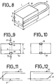
- FIG. 8 is an isometric view of a two-wire resonator according to the invention.
- the resonator includes a dielectric rod 50 having the shape of a rectangular parallelepiped of length and cross section axb as indicated in the figure.
- the resonator also includes the jumper or armature 51 of length L which encloses the rod 50 by embedding and which constitutes both the two electrodes of the resonator and their short-circuit.
- the jumper 51 can have different shapes, for example in the shape of a U as shown in FIG. 8.
- the resonant frequency and the overvoltage coefficient Q are mainly determined by the length L of the electrodes, the distance between these electrodes and the nature of the dielectric.
- the length of the bar 50 can be reduced to approximately without appreciable alteration of the main characteristics of the resonator.
- the first method leads to poor overvoltage coefficients and unstable resonance frequencies due to the thickness of the adhesive joint and the dielectric losses of the insulating adhesive.
- the second method provides better performance because the joint is thinner and the dielectric losses of this kind of glue are lower.
- the sintered conductive adhesive of the third method ensures excellent contact and therefore good frequency stability. However, due to its poor conductivity, it is difficult to obtain a very low surface resistance and the overvoltage is degraded.
- the size of the glue affects the value of the resonant frequency. If the glued area increases, the resonant frequency decreases. We can take advantage of this property and increase the conductive bonded surface taking into account the influences of the external metal parts (case, cover) to lower the resonant frequency by a factor of 2 or 3 without increasing the bulk.
- the embedding technique of the fourth method makes it possible to obtain the highest overvoltages.
- the frequency stability depends a lot on the quality of the embedding.
- the best results are obtained by hot punching under a neutral atmosphere, for example at 500 ° C. under nitrogen, optionally followed by an aging stage carried out under the same conditions.
- the duration of the landing can be of the order of one hour.
- Figure 9 shows the same resonator as that shown in Figure 8 but seen at one of its ends.
- the jumper 51 is placed in a housing 52 intended to receive it and made in the bar 50.
- the punches 53 act on the jumper 51 in the direction indicated by the arrows in order to embed the jumper.
- Figure 10 shows the result obtained after punching.
- the fifth method, in situ molding, requires the use of dielectric parts forming the negative impression of the metal part. This can be preformed and placed in the dielectric. The whole is brought to a temperature slightly higher than the melting temperature of the metal and then cooled slowly. Silver works particularly well.
- the jumper is made of copper and is embedded by punching. Under these conditions, the overvoltage coefficient Q is equal to 1000 at the frequency of 950 MHz. This is a very good result given the size of the resonator.
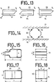
- FIG. 13 schematically represents the arrangement envisaged for a filter with three resonators 70, 73 and 76 They are quarter wave resonators with two resonances. They are formed as for FIG. 12 of metallic reinforcements enclosing a dielectric bar not shown and situated in planes perpendicular to one another.
- the resonator 70 includes the pairs of frames 71 and 72
- the resonator 73 includes the couples 74 and 75
- the resonator 76 includes the couples 77 and 78.
- the resonators are placed in the extension of each other as shown in Figure 13.
- the armatures 71 and 74 located in the same plane or in parallel planes provide a preponderant magnetic coupling between the resonators 70 and 73.
- the value of these couplings is adjusted by the distances between resonators.
- the input signal is injected via a coupling loop at the pole P 1 .
- the output signal is extracted in the same way at the P ⁇ pole. Couplings of the intra-resonator type are rather ensured by the electric fields in the dielectric and are regulated by the defects of symmetry of the resonator (defect of orthogonality of two armatures, influence of the case, etc.).
- the resonators which can be used in this type of filter can be produced using techniques described for the manufacture of biruban or bifilar resonators.
- the very section of the dielectric is determined by additional considerations (heat dissipation, convenience of fixing) and can be square, round, octagonal.
- FIG. 14 represents the octagonal section of a dielectric bar 80 equipped with two armatures 83 and 84 placed in perpendicular planes. The resonator thus formed can be conveniently placed between two metal surfaces 81 and 82.
- FIGS. 17 and 18 represent front and side views of a quarter wave resonator formed by a dielectric bar 95 covered with a metallization 96 on two opposite faces and one end. Again the resonator includes sections of different areas. The inter-electrode width remains constant but it is the transverse dimension of the bar which changes. This dimension which is worth b near the open circuit, is worth b ' ⁇ b near the short circuit. This has the consequence of increasing the inductance and therefore of decreasing the resonant frequency.
- the dielectric material it is essential to choose the dielectric material so as to compensate for thermal drifts.
- the coefficient expressing the first order drift in temperature equal to 0 ppm / ° C.
- the reinforcement is only partially secured to the dielectric, it is necessary to compensate for the expansion of the metal by choosing coefficients typically between + 10 and 20 ppm / ° C. Dielectrics having these characteristics have been described in the French patent published under the number FR-A-2 477 823.
Landscapes
- Control Of Motors That Do Not Use Commutators (AREA)
Claims (18)
Applications Claiming Priority (2)
| Application Number | Priority Date | Filing Date | Title |
|---|---|---|---|
| FR8418640 | 1984-12-06 | ||
| FR8418640A FR2568414B1 (fr) | 1984-05-25 | 1984-12-06 | Resonateurs electromagnetiques et filtres realises a partir de ces resonateurs. |
Publications (2)
| Publication Number | Publication Date |
|---|---|
| EP0187579A1 EP0187579A1 (de) | 1986-07-16 |
| EP0187579B1 true EP0187579B1 (de) | 1989-05-10 |
Family
ID=9310314
Family Applications (1)
| Application Number | Title | Priority Date | Filing Date |
|---|---|---|---|
| EP19850402432 Expired EP0187579B1 (de) | 1984-12-06 | 1985-12-06 | Elektromagnetische Resonatoren und Filter mit solchen Resonatoren |
Country Status (2)
| Country | Link |
|---|---|
| EP (1) | EP0187579B1 (de) |
| DE (1) | DE3570156D1 (de) |
Family Cites Families (7)
| Publication number | Priority date | Publication date | Assignee | Title |
|---|---|---|---|---|
| NL43088C (de) * | 1934-07-09 | |||
| DE940052C (de) * | 1952-10-01 | 1956-03-08 | Siemens Ag | Anordnung zur mechanischen Abstuetzung von Schwingspulen von hochfrequenten Kreisen |
| US2838736A (en) * | 1953-03-20 | 1958-06-10 | Erie Resistor Corp | High dielectric constant cavity resonator |
| CH322835A (de) * | 1954-04-20 | 1957-06-30 | Patelhold Patentverwertung | Einrichtung zur veränderbaren Kopplung zweier Lecherleitungen |
| US2832892A (en) * | 1954-12-24 | 1958-04-29 | Du Mont Allen B Lab Inc | Tuning device for ultra-high frequency circuits |
| US2894225A (en) * | 1956-10-29 | 1959-07-07 | Jr James Elmer Myers | Tuning apparatus |
| FR2535547B1 (fr) * | 1982-10-29 | 1988-09-16 | Thomson Csf | Resonateurs bi-rubans et filtres realises a partir de ces resonateurs |
-
1985
- 1985-12-06 DE DE8585402432T patent/DE3570156D1/de not_active Expired
- 1985-12-06 EP EP19850402432 patent/EP0187579B1/de not_active Expired
Also Published As
| Publication number | Publication date |
|---|---|
| DE3570156D1 (en) | 1989-06-15 |
| EP0187579A1 (de) | 1986-07-16 |
Similar Documents
| Publication | Publication Date | Title |
|---|---|---|
| FR2568414A1 (fr) | Resonateurs electromagnetiques et filtres realises a partir de ces resonateurs. | |
| EP0123350B1 (de) | Flache Mikrowellenantenne mit einer völlig hängenden Mikrostreifengruppe | |
| EP2345104B1 (de) | Differenz-dipolantennensystem mit einer koplanaren strahlungsstruktur und sender-/empfängereinrichtung | |
| EP0667984B1 (de) | Monopolantenne mit platten- und stabstrahlern | |
| EP1238431A1 (de) | Verfahren und vorrichtung zur dreidimensionalen verbindung elektronischer komponenten | |
| FR2989842A1 (fr) | Ligne de propagation radiofrequence a ondes lentes | |
| EP0108003B1 (de) | Doppelstreifen-Resonator und nach dieser Art gestaltetes Filter | |
| EP0165158A1 (de) | Dielektrischer Filter mit veränderbarer Mittenfrequenz | |
| EP0616490A1 (de) | Miniaturisierte elektronische Anordnung, insbesondere mit gyromagnetischem Effekt | |
| EP0260633A1 (de) | Aus verschiedenen Elementen bestehendes Filter der E-Flächenart | |
| EP1231615A1 (de) | Struktur einer integrierten Induktivität | |
| EP0424255B1 (de) | Filtereinheit und entsprechender Filter | |
| EP0101369A1 (de) | Banddurchlassfilter mit dielektrischen Resonatoren, mit negativer Kupplung zwischen Resonatoren | |
| EP1202376A1 (de) | Elektrischer Resonator | |
| EP0169122A1 (de) | Mittels Gleichspannung steuerbares Element mit variabler Kapazität | |
| EP0586010B1 (de) | Hochfrequenzschaltung und Verfahren zur deren Herstellung | |
| EP0187579A1 (de) | Elektromagnetische Resonatoren und Filter mit solchen Resonatoren | |
| EP0223673B1 (de) | Kopplungsvorrichtung zwischen einer Übertragungsleitung elektromagnetischer Oberflächenwellen und einer Mikrostreifenleitung | |
| FR2721431A1 (fr) | Procédé pour réaliser des composants magnétiques à bobinages simplifiés, et composants ainsi réalisés. | |
| WO2019110651A1 (fr) | Composant micro-ondes et procédé de fabrication associé | |
| EP0649571B1 (de) | Bandpassfilter mit gekoppelten resonatoren | |
| EP2688137B1 (de) | Hyperfrequenzresonator mit Impedanzsprung, insbesondere für Hyperfrequenz-Bandsperrfilter oder -Bandpassfilter | |
| FR2536211A1 (fr) | Structure de diode hyperfrequences dont les connexions exterieures sont prises par deux poutres metalliques | |
| FR2828337A1 (fr) | Circuit resonant hyperfrequence et filtre hyperfrequence accordable utilisant le circuit resonant | |
| FR2521786A2 (fr) | Filtre passe-bande a resonateurs dielectriques |
Legal Events
| Date | Code | Title | Description |
|---|---|---|---|
| PUAI | Public reference made under article 153(3) epc to a published international application that has entered the european phase |
Free format text: ORIGINAL CODE: 0009012 |
|
| AK | Designated contracting states |
Kind code of ref document: A1 Designated state(s): DE GB IT NL SE |
|
| 17P | Request for examination filed |
Effective date: 19870103 |
|
| 17Q | First examination report despatched |
Effective date: 19880921 |
|
| GRAA | (expected) grant |
Free format text: ORIGINAL CODE: 0009210 |
|
| AK | Designated contracting states |
Kind code of ref document: B1 Designated state(s): DE GB IT NL SE |
|
| ITF | It: translation for a ep patent filed | ||
| RAP4 | Party data changed (patent owner data changed or rights of a patent transferred) |
Owner name: THOMSON-CSF |
|
| REF | Corresponds to: |
Ref document number: 3570156 Country of ref document: DE Date of ref document: 19890615 |
|
| GBT | Gb: translation of ep patent filed (gb section 77(6)(a)/1977) | ||
| PLBE | No opposition filed within time limit |
Free format text: ORIGINAL CODE: 0009261 |
|
| STAA | Information on the status of an ep patent application or granted ep patent |
Free format text: STATUS: NO OPPOSITION FILED WITHIN TIME LIMIT |
|
| 26N | No opposition filed | ||
| PGFP | Annual fee paid to national office [announced via postgrant information from national office to epo] |
Ref country code: DE Payment date: 19921112 Year of fee payment: 8 |
|
| PGFP | Annual fee paid to national office [announced via postgrant information from national office to epo] |
Ref country code: SE Payment date: 19921113 Year of fee payment: 8 |
|
| PGFP | Annual fee paid to national office [announced via postgrant information from national office to epo] |
Ref country code: GB Payment date: 19921118 Year of fee payment: 8 |
|
| ITTA | It: last paid annual fee | ||
| PGFP | Annual fee paid to national office [announced via postgrant information from national office to epo] |
Ref country code: NL Payment date: 19921231 Year of fee payment: 8 |
|
| PG25 | Lapsed in a contracting state [announced via postgrant information from national office to epo] |
Ref country code: GB Effective date: 19931206 |
|
| PG25 | Lapsed in a contracting state [announced via postgrant information from national office to epo] |
Ref country code: SE Effective date: 19931207 |
|
| PG25 | Lapsed in a contracting state [announced via postgrant information from national office to epo] |
Ref country code: NL Effective date: 19940701 |
|
| GBPC | Gb: european patent ceased through non-payment of renewal fee |
Effective date: 19931206 |
|
| NLV4 | Nl: lapsed or anulled due to non-payment of the annual fee | ||
| PG25 | Lapsed in a contracting state [announced via postgrant information from national office to epo] |
Ref country code: DE Effective date: 19940901 |
|
| EUG | Se: european patent has lapsed |
Ref document number: 85402432.0 Effective date: 19940710 |