EP0223673B1 - Kopplungsvorrichtung zwischen einer Übertragungsleitung elektromagnetischer Oberflächenwellen und einer Mikrostreifenleitung - Google Patents
Kopplungsvorrichtung zwischen einer Übertragungsleitung elektromagnetischer Oberflächenwellen und einer Mikrostreifenleitung Download PDFInfo
- Publication number
- EP0223673B1 EP0223673B1 EP86402348A EP86402348A EP0223673B1 EP 0223673 B1 EP0223673 B1 EP 0223673B1 EP 86402348 A EP86402348 A EP 86402348A EP 86402348 A EP86402348 A EP 86402348A EP 0223673 B1 EP0223673 B1 EP 0223673B1
- Authority
- EP
- European Patent Office
- Prior art keywords
- microstrip
- dielectric
- coupling device
- component
- line
- Prior art date
- Legal status (The legal status is an assumption and is not a legal conclusion. Google has not performed a legal analysis and makes no representation as to the accuracy of the status listed.)
- Expired - Lifetime
Links
- 230000008878 coupling Effects 0.000 title claims description 40
- 238000010168 coupling process Methods 0.000 title claims description 40
- 238000005859 coupling reaction Methods 0.000 title claims description 40
- 230000005540 biological transmission Effects 0.000 title claims 4
- 239000003989 dielectric material Substances 0.000 claims description 16
- 230000007704 transition Effects 0.000 claims description 16
- 229910052751 metal Inorganic materials 0.000 claims description 15
- 239000002184 metal Substances 0.000 claims description 15
- 239000000463 material Substances 0.000 claims description 6
- 239000000758 substrate Substances 0.000 claims description 5
- PNEYBMLMFCGWSK-UHFFFAOYSA-N aluminium oxide Inorganic materials [O-2].[O-2].[O-2].[Al+3].[Al+3] PNEYBMLMFCGWSK-UHFFFAOYSA-N 0.000 claims description 3
- -1 polytetrafluoroethylene Polymers 0.000 claims description 3
- 229920001343 polytetrafluoroethylene Polymers 0.000 claims description 3
- 239000004810 polytetrafluoroethylene Substances 0.000 claims description 3
- 229910001369 Brass Inorganic materials 0.000 claims description 2
- 229910000906 Bronze Inorganic materials 0.000 claims description 2
- 239000000853 adhesive Substances 0.000 claims description 2
- 230000001070 adhesive effect Effects 0.000 claims description 2
- 229910052790 beryllium Inorganic materials 0.000 claims description 2
- ATBAMAFKBVZNFJ-UHFFFAOYSA-N beryllium atom Chemical compound [Be] ATBAMAFKBVZNFJ-UHFFFAOYSA-N 0.000 claims description 2
- 239000010951 brass Substances 0.000 claims description 2
- 239000010974 bronze Substances 0.000 claims description 2
- KUNSUQLRTQLHQQ-UHFFFAOYSA-N copper tin Chemical compound [Cu].[Sn] KUNSUQLRTQLHQQ-UHFFFAOYSA-N 0.000 claims description 2
- 239000003365 glass fiber Substances 0.000 claims description 2
- 239000000696 magnetic material Substances 0.000 claims 2
- 101100400378 Mus musculus Marveld2 gene Proteins 0.000 claims 1
- 229910010293 ceramic material Inorganic materials 0.000 claims 1
- 230000000750 progressive effect Effects 0.000 claims 1
- 239000012212 insulator Substances 0.000 description 16
- 230000006978 adaptation Effects 0.000 description 14
- 229910000859 α-Fe Inorganic materials 0.000 description 14
- 238000001465 metallisation Methods 0.000 description 6
- 239000011521 glass Substances 0.000 description 3
- 230000003071 parasitic effect Effects 0.000 description 3
- BQCADISMDOOEFD-UHFFFAOYSA-N Silver Chemical compound [Ag] BQCADISMDOOEFD-UHFFFAOYSA-N 0.000 description 2
- 229910000831 Steel Inorganic materials 0.000 description 2
- 240000008042 Zea mays Species 0.000 description 2
- 230000002745 absorbent Effects 0.000 description 2
- 239000002250 absorbent Substances 0.000 description 2
- 239000011324 bead Substances 0.000 description 2
- 238000003780 insertion Methods 0.000 description 2
- 230000037431 insertion Effects 0.000 description 2
- 230000001902 propagating effect Effects 0.000 description 2
- 229910052709 silver Inorganic materials 0.000 description 2
- 239000004332 silver Substances 0.000 description 2
- 239000010959 steel Substances 0.000 description 2
- FRWYFWZENXDZMU-UHFFFAOYSA-N 2-iodoquinoline Chemical compound C1=CC=CC2=NC(I)=CC=C21 FRWYFWZENXDZMU-UHFFFAOYSA-N 0.000 description 1
- LTPBRCUWZOMYOC-UHFFFAOYSA-N beryllium oxide Inorganic materials O=[Be] LTPBRCUWZOMYOC-UHFFFAOYSA-N 0.000 description 1
- 238000006243 chemical reaction Methods 0.000 description 1
- 239000011248 coating agent Substances 0.000 description 1
- 238000000576 coating method Methods 0.000 description 1
- 239000000470 constituent Substances 0.000 description 1
- 238000010276 construction Methods 0.000 description 1
- 238000010586 diagram Methods 0.000 description 1
- 238000005530 etching Methods 0.000 description 1
- 230000005284 excitation Effects 0.000 description 1
- 239000012634 fragment Substances 0.000 description 1
- 238000009413 insulation Methods 0.000 description 1
- 230000010354 integration Effects 0.000 description 1
- 238000002955 isolation Methods 0.000 description 1
- 238000000034 method Methods 0.000 description 1
- 230000010355 oscillation Effects 0.000 description 1
- 230000000284 resting effect Effects 0.000 description 1
Images
Classifications
-
- H—ELECTRICITY
- H01—ELECTRIC ELEMENTS
- H01P—WAVEGUIDES; RESONATORS, LINES, OR OTHER DEVICES OF THE WAVEGUIDE TYPE
- H01P5/00—Coupling devices of the waveguide type
- H01P5/08—Coupling devices of the waveguide type for linking dissimilar lines or devices
Definitions
- the present invention relates to a coupling device between a surface wave line and a microstrip line. More specifically, it relates to a coupling device between a microstrip line, in which the field distribution is asymmetrical, operating in quasi-TEM mode, and an access line to a device, in which the field distribution is symmetrical, using an electromagnetic surface mode propagating in a thin core line, charged by ferrite parts, and polarized by a magnetostatic field, such as an insulator or non-reciprocal ferrite device.
- An object of the invention is to make this non-reciprocal device integrable, and to do without the coaxial connectors which until now were used, because these are too bulky for integration.
- a known technique giving satisfactory results but delicate to implement and therefore not very usable, consists in integrating, on the two access lines to the surface wave device, a coaxial line element, in the form of a pearl. glass adapted to 50 ohms, which amounts to reconstructing the excitation system of the electromagnetic surface wave mode used in known devices.
- this glass bead introduces parasitic elements disturbing the adaptation of the device.
- the adaptation system, or coupling device consists in using, to make the transition between the thin core and the microstrip line, several line elements of short lengths and of small transverse dimensions compared to the length of wave, these elements being of different types and structures so as to achieve a gradual symmetry-asymmetry transition, in stages, the element closest to the thin core being necessarily symmetrical and of small transverse dimensions so as to impose a structure symmetric field of view at the access to the thin core line.
- the coupling device according to the invention has the merit of remaining continuous throughout the conductive cores in flat structure, therefore of reducing to their lowest expression the parasitic elements due to the discontinuities between the central core 12 and an external microstrip line.
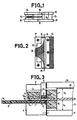
- This coupling device is shown in section in Figure 3, while Figure 4 shows it in plan, mounted on an OSEL isolator and allows a better understanding of the design.
- FIG. 3 appears - to the right of the figure - a fragment of the OSEL insulator, comprising a thin core 12, clamped between two thin ferrite plates 10 and 11, themselves clamped between two steel plates 16 and 17.
- the thickness of each of the plates 16 and 17 is sufficient for it to be possible to drill therein, longitudinally, a tapped hole for fixing the coupling device.
- the end 19 of the central core 12 protrudes from the insulator over a length of the order of 2.5 to 3 mm: it is on this end 19 that contact will be made with an external microstrip 9.
- L isolator further comprises, in known manner, two parts 7 and 8, placed between the ferrite plates 10-11 and the coupling device: these parts 7 and 8 are made of dielectric material of constant e 2 and are used for the adaptation of the OSEL insulator.
- the coupling device proper comprises the three parts marked 1, 2 and 3, and their respective mechanical supports 4, 5 and 6.
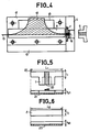
- the part 1 is a part made of dielectric material of polytetrafluoroethylene type loaded with glass fiber, such as that known under the name of RT Duroid, but it can also be for example made of alumina or beryllium oxide.
- Its permittivity P-1 is the same as that of the support of the external microstrip piece 9 and that of the piece 2 which will be described later.
- This part 1 has a T shape (see fig 5) and it is metallized on its two main faces, to give a ground plane 21 on one side and, after etching, a metallization 20 on the other face.
- the transverse branch 22 of the T has a length Li, a width 11 , and a thickness of dielectric h dl .
- the part 1 is attached to the OSEL insulator by its transverse branch 22, and the end 19 of the central core 12 comes to rest on the metallization 20.
- the etched metal track 20 may have an enlarged part. This enlarged part participates, with the dielectric part 3, in the adaptation in the transition between the symmetrical and asymmetrical modes.
- the part 3 is a parallelepiped of dielectric material of permittivity es, the thickness of dielectric of which is h d3 and the width 1 3 , measured along the axis common to the end 19 of the core 12 and to the external microstrip 9
- the dimensions of the part 3 are such that, when it is placed on the end 19 of the core 12, which constitutes a microstrip, it projects beyond this microstrip, in order to allow adaptation between the two microstrips 19 and 9. It is made of polytetrafluoroethylene, or alumina.
- All of these three parts 1, 2 and 3 of dielectric material are mechanically held in place by three other non-magnetic metal parts, respectively 4, 5 and 6.
- These are for example brass or silver beryllium bronze, shade UBe 2.
- the part 4 constitutes the support of the coupling device according to the invention. It is integral with the insulator, or more exactly with a plate 17, and ensures its correct mounting on a ground plane.
- This support 4 supports the part 1 of dielectric material, itself in contact by its etched metal track 20 with a first face of the microstrip 19 of the central core 12.
- the part 5 is, like the support 4, integral with the insulator, and more exactly with the plate 16. This pressure part 5 holds in place the part 2 made of dielectric material, and presses it on a second face of the microstrip 19 of the central core 12, the metallization 23 of the part 2 being in contact with said microstrip 19.
- the support 4 and the pressure piece 5 both have a housing which makes it possible to position the two dielectric pieces 1 and 2, and prevents their lateral sliding relative to the microstrip line 19.
- the part 6 is a stirrup, secured to the support 4: it makes it possible to maintain the dielectric block 3, against the microstrip 19, and participates in the adaptation of the coupling device.
- the dimensions of the dielectric and metallic parts, and in particular of the support 4, with respect to the microstrip 19, are such that they allow the end of an external microstrip 9 to be introduced into the housing provided in the support 4 for the part.
- the microstrip 9 comprises a substrate, of permittivity ei, a metallization of a ground plane on a main face of the substrate, and the metallic track of the microstrip line on the other main face of the substrate: it is in the form of a tongue.
- This external microstrip line 9 rests - when it is in place - by its ground plane on the support 4; it abuts against the dielectric part 1, and the microstrip line proper is in contact with the end 19 of the central core 12.
- the dielectric block 3 and the stirrup 6 support the end 19 of the core central 12 against the microstrip 9. So that the electrical contact is good, the end 19 is glued to the microstrip 9 by means of a conductive adhesive. In a variant, the end 19 can slide on the microstrip 9 during large temperature variations.
- Figure 4 completes Figure 3, showing, seen in plan, an isolator provided with the coupling device according to the invention, as well as an external microstrip line about to be connected to the coupler.
- the insulator is cut at the level of the central core 12 and, for the coupler, the dielectric parts 2 and 3 as well as the metal parts 5 and 6 are removed.
- the coupling is obtained by using several line elements of small width and of small transverse dimensions compared to the wavelength, the type and the structure of these elements being different so as to achieve a gradual transition, in stages. , between the symmetrical or asymmetrical distribution of the fields.
- the isolator requires that the line element which is closest to it is symmetrical.
- Maintaining the width of the central core throughout the transition at values very close to that of the coupling level is an essential point of the transition.
- the dimensions (1 1 , 1 2 , 1 3 , 1 4 and h d s) of the other parts are adjusted to maintain the necessary impedance level, that is to say generally close to 50 ohms.
- the invention has been explained by relying on the case of an OSEL isolator, and by describing and representing only one coupling device. It is obvious to a person skilled in the art that if the symmetrical device has more than one external connection, it is provided with the appropriate number of devices for coupling to an external microstrip line.
- the insulator of FIG. 4 comprises in its embodiment a coupler on the end 18 of the central core and a coupler on the end 19.
- the second access can be equipped with a corrector.
- the coupling device according to the invention operates at least in the frequency range 6 - 18 GHz, with insertion losses of less than 1.6 dB and a standing wave ratio at the ports of less than 1.35.
Landscapes
- Waveguides (AREA)
- Control Of Motors That Do Not Use Commutators (AREA)
- Seal Device For Vehicle (AREA)
- Physical Deposition Of Substances That Are Components Of Semiconductor Devices (AREA)
Claims (16)


Applications Claiming Priority (2)
| Application Number | Priority Date | Filing Date | Title |
|---|---|---|---|
| FR8515880 | 1985-10-25 | ||
| FR8515880A FR2589283B1 (fr) | 1985-10-25 | 1985-10-25 | Dispositif de couplage entre une ligne a ondes de surface electromagnetique et une ligne microbande exterieure |
Publications (2)
| Publication Number | Publication Date |
|---|---|
| EP0223673A1 EP0223673A1 (de) | 1987-05-27 |
| EP0223673B1 true EP0223673B1 (de) | 1990-08-08 |
Family
ID=9324201
Family Applications (1)
| Application Number | Title | Priority Date | Filing Date |
|---|---|---|---|
| EP86402348A Expired - Lifetime EP0223673B1 (de) | 1985-10-25 | 1986-10-20 | Kopplungsvorrichtung zwischen einer Übertragungsleitung elektromagnetischer Oberflächenwellen und einer Mikrostreifenleitung |
Country Status (7)
| Country | Link |
|---|---|
| US (1) | US4733202A (de) |
| EP (1) | EP0223673B1 (de) |
| JP (1) | JPS62102603A (de) |
| CA (1) | CA1256518A (de) |
| DE (1) | DE3673340D1 (de) |
| ES (1) | ES2016267B3 (de) |
| FR (1) | FR2589283B1 (de) |
Families Citing this family (7)
| Publication number | Priority date | Publication date | Assignee | Title |
|---|---|---|---|---|
| US4870375A (en) * | 1987-11-27 | 1989-09-26 | General Electric Company | Disconnectable microstrip to stripline transition |
| US4862120A (en) * | 1988-02-29 | 1989-08-29 | Canadian Patents And Development Limited/Societe Canadienne Des Brevets Et D'exploitation Limitee | Wideband stripline to microstrip transition |
| FR2687852A1 (fr) * | 1992-02-26 | 1993-08-27 | Dassault Electronique | Dispositif de connexion entre une antenne et un boitier de microelectronique. |
| JP3475195B2 (ja) | 1995-03-03 | 2003-12-08 | ミネベア株式会社 | ブラシレスdcモ−タ |
| FI98105C (fi) * | 1995-03-06 | 1997-04-10 | Valtion Teknillinen | Mikroliuska-aaltoputkisiirtymä |
| US6692267B1 (en) * | 2001-08-23 | 2004-02-17 | Ciena Corporation | Printed circuit board testing module |
| US7916067B2 (en) * | 2009-02-11 | 2011-03-29 | The Boeing Company | Removing clutter from radar cross section measurements using spectral tagging |
Family Cites Families (5)
| Publication number | Priority date | Publication date | Assignee | Title |
|---|---|---|---|---|
| US3617951A (en) * | 1968-11-21 | 1971-11-02 | Western Microwave Lab Inc | Broadband circulator or isolator of the strip line or microstrip type |
| US3662318A (en) * | 1970-12-23 | 1972-05-09 | Comp Generale Electricite | Transition device between coaxial and microstrip lines |
| DE2226726C3 (de) * | 1971-06-04 | 1982-05-27 | Lignes Télégraphiques et Téléphoniques, Paris | Nichtreziproke Übertragungsanordnung für elektromagnetische Höchstfrequenzwellen |
| US3886502A (en) * | 1974-08-06 | 1975-05-27 | Ryt Ind | Broad band field displacement isolator |
| JPS5597702A (en) * | 1979-01-22 | 1980-07-25 | Mitsubishi Electric Corp | Waveguide-coupled microwave integrated-circuit device |
-
1985
- 1985-10-25 FR FR8515880A patent/FR2589283B1/fr not_active Expired
-
1986
- 1986-10-20 EP EP86402348A patent/EP0223673B1/de not_active Expired - Lifetime
- 1986-10-20 DE DE8686402348T patent/DE3673340D1/de not_active Expired - Fee Related
- 1986-10-20 ES ES86402348T patent/ES2016267B3/es not_active Expired - Lifetime
- 1986-10-22 US US06/921,426 patent/US4733202A/en not_active Expired - Fee Related
- 1986-10-24 CA CA000521421A patent/CA1256518A/en not_active Expired
- 1986-10-24 JP JP61252109A patent/JPS62102603A/ja active Pending
Also Published As
| Publication number | Publication date |
|---|---|
| FR2589283B1 (fr) | 1987-11-20 |
| ES2016267B3 (es) | 1990-11-01 |
| US4733202A (en) | 1988-03-22 |
| JPS62102603A (ja) | 1987-05-13 |
| CA1256518A (en) | 1989-06-27 |
| EP0223673A1 (de) | 1987-05-27 |
| FR2589283A1 (fr) | 1987-04-30 |
| DE3673340D1 (de) | 1990-09-13 |
Similar Documents
| Publication | Publication Date | Title |
|---|---|---|
| EP0123350B1 (de) | Flache Mikrowellenantenne mit einer völlig hängenden Mikrostreifengruppe | |
| EP0924797B1 (de) | Multifrequenzstreifenleitungsantenne und Gerät mit einer derartigen Antenne | |
| EP0954055A1 (de) | Antenne für zwei Frequenzen für die Radiokommunikation in Form einer Mikrostreifenleiterantenne | |
| FR2797352A1 (fr) | Antenne a empilement de structures resonantes et dispositif de radiocommunication multifrequence incluant cette antenne | |
| EP0134611B1 (de) | Sende- oder Empfangsstrahlergruppe einer Mikrowellenflachantenne und Sende- oder Empfangseinrichtung von Mikrowellensignalen mit einer solchen Flachantenne | |
| FR2623020A1 (fr) | Dispositif d'excitation d'un guide d'onde en polarisation circulaire par une antenne plane | |
| EP0193162A1 (de) | Mikrowellenbandpassfilter | |
| EP1250729B1 (de) | Antenne mit anisotroper verbundstoff | |
| EP0223673B1 (de) | Kopplungsvorrichtung zwischen einer Übertragungsleitung elektromagnetischer Oberflächenwellen und einer Mikrostreifenleitung | |
| EP0446107B1 (de) | Übertragungssystem für elektrische Energie, im Mikrowellenbereich, mit kreismagnetischem Effekt, wie ein Zirkulator, Isolator oder Filter | |
| EP0582637B1 (de) | Mikrostreifenleiter/wellenleiter übergang | |
| EP0023873B1 (de) | Passiver Leistungsbegrenzer mit Halbleitern und als Streifenleitung ausgeführt und Mikrowellenschaltung mit einem solchen Begrenzer | |
| EP0387955A1 (de) | Gehäuse für eine integrierte Hyperfrequenzschaltung | |
| EP0044758B1 (de) | Abschlussvorrichtung für eine Mikrowellenleitung mit minimalem Stehwellenfaktor | |
| FR2462787A1 (fr) | Dispositif de transition entre une ligne hyperfrequence et un guide d'onde et source hyperfrequence comprenant une telle transition | |
| FR2685130A1 (fr) | Antenne pastille carree a deux polarisations croisees excitee par deux fentes orthogonales. | |
| EP0127526A1 (de) | Filtereinrichtung mit magnetostatischer Welle | |
| EP0073165B1 (de) | Mikrowellenschalter | |
| EP0334270B1 (de) | Mikrowellen-Anpassungsvorrichtung für einen Übergang zwischen einem Hohlleiter und einer Planarleitung | |
| FR2871618A1 (fr) | Filtre basse-bande hyperfrequence de type finline | |
| EP0430136A1 (de) | Bandsperrfilter für Mikrowellenhohlleiter | |
| EP0296929B1 (de) | Symmetrische Mikrowellenübertragungsleitung mit zwei koplanären Leitern | |
| EP0109895B1 (de) | Koaxiale Hochfrequenzlast, Einwegleitung in Triplatetechnik mit einer solchen Last und Verwendung einer solchen Einwegleitung | |
| FR2828337A1 (fr) | Circuit resonant hyperfrequence et filtre hyperfrequence accordable utilisant le circuit resonant | |
| EP0100274B1 (de) | Anpassungs- und Einweganordnung mit Ferritzirkulator |
Legal Events
| Date | Code | Title | Description |
|---|---|---|---|
| PUAI | Public reference made under article 153(3) epc to a published international application that has entered the european phase |
Free format text: ORIGINAL CODE: 0009012 |
|
| AK | Designated contracting states |
Kind code of ref document: A1 Designated state(s): BE DE ES GB IT NL SE |
|
| 17P | Request for examination filed |
Effective date: 19870609 |
|
| RAP3 | Party data changed (applicant data changed or rights of an application transferred) |
Owner name: THOMSON-CSF |
|
| 17Q | First examination report despatched |
Effective date: 19900108 |
|
| GRAA | (expected) grant |
Free format text: ORIGINAL CODE: 0009210 |
|
| AK | Designated contracting states |
Kind code of ref document: B1 Designated state(s): BE DE ES GB IT NL SE |
|
| ITF | It: translation for a ep patent filed | ||
| GBT | Gb: translation of ep patent filed (gb section 77(6)(a)/1977) | ||
| REF | Corresponds to: |
Ref document number: 3673340 Country of ref document: DE Date of ref document: 19900913 |
|
| PLBE | No opposition filed within time limit |
Free format text: ORIGINAL CODE: 0009261 |
|
| STAA | Information on the status of an ep patent application or granted ep patent |
Free format text: STATUS: NO OPPOSITION FILED WITHIN TIME LIMIT |
|
| 26N | No opposition filed | ||
| PGFP | Annual fee paid to national office [announced via postgrant information from national office to epo] |
Ref country code: GB Payment date: 19910920 Year of fee payment: 6 |
|
| PGFP | Annual fee paid to national office [announced via postgrant information from national office to epo] |
Ref country code: SE Payment date: 19910923 Year of fee payment: 6 |
|
| PGFP | Annual fee paid to national office [announced via postgrant information from national office to epo] |
Ref country code: DE Payment date: 19910924 Year of fee payment: 6 |
|
| PGFP | Annual fee paid to national office [announced via postgrant information from national office to epo] |
Ref country code: ES Payment date: 19911009 Year of fee payment: 6 |
|
| PGFP | Annual fee paid to national office [announced via postgrant information from national office to epo] |
Ref country code: BE Payment date: 19911022 Year of fee payment: 6 |
|
| ITTA | It: last paid annual fee | ||
| PGFP | Annual fee paid to national office [announced via postgrant information from national office to epo] |
Ref country code: NL Payment date: 19911031 Year of fee payment: 6 |
|
| PG25 | Lapsed in a contracting state [announced via postgrant information from national office to epo] |
Ref country code: GB Effective date: 19921020 |
|
| PG25 | Lapsed in a contracting state [announced via postgrant information from national office to epo] |
Ref country code: SE Effective date: 19921021 Ref country code: ES Free format text: LAPSE BECAUSE OF EXPIRATION OF PROTECTION Effective date: 19921021 |
|
| PG25 | Lapsed in a contracting state [announced via postgrant information from national office to epo] |
Ref country code: BE Effective date: 19921031 |
|
| BERE | Be: lapsed |
Owner name: THOMSON-CSF Effective date: 19921031 |
|
| PG25 | Lapsed in a contracting state [announced via postgrant information from national office to epo] |
Ref country code: NL Effective date: 19930501 |
|
| GBPC | Gb: european patent ceased through non-payment of renewal fee |
Effective date: 19921020 |
|
| NLV4 | Nl: lapsed or anulled due to non-payment of the annual fee | ||
| PG25 | Lapsed in a contracting state [announced via postgrant information from national office to epo] |
Ref country code: DE Effective date: 19930701 |
|
| EUG | Se: european patent has lapsed |
Ref document number: 86402348.6 Effective date: 19930510 |
|
| REG | Reference to a national code |
Ref country code: ES Ref legal event code: FD2A Effective date: 19990601 |
|
| PG25 | Lapsed in a contracting state [announced via postgrant information from national office to epo] |
Ref country code: IT Free format text: LAPSE BECAUSE OF NON-PAYMENT OF DUE FEES;WARNING: LAPSES OF ITALIAN PATENTS WITH EFFECTIVE DATE BEFORE 2007 MAY HAVE OCCURRED AT ANY TIME BEFORE 2007. THE CORRECT EFFECTIVE DATE MAY BE DIFFERENT FROM THE ONE RECORDED. Effective date: 20051020 |