EP0187985A1 - Méthode et disposition de circuit pour réaliser un dispositif à commande séquentielle en utilisant une mémoire à boucle fermée - Google Patents
Méthode et disposition de circuit pour réaliser un dispositif à commande séquentielle en utilisant une mémoire à boucle fermée Download PDFInfo
- Publication number
- EP0187985A1 EP0187985A1 EP85116280A EP85116280A EP0187985A1 EP 0187985 A1 EP0187985 A1 EP 0187985A1 EP 85116280 A EP85116280 A EP 85116280A EP 85116280 A EP85116280 A EP 85116280A EP 0187985 A1 EP0187985 A1 EP 0187985A1
- Authority
- EP
- European Patent Office
- Prior art keywords
- memory
- outputs
- feedback
- inputs
- circuit
- Prior art date
- Legal status (The legal status is an assumption and is not a legal conclusion. Google has not performed a legal analysis and makes no representation as to the accuracy of the status listed.)
- Withdrawn
Links
Images


Classifications
-
- G—PHYSICS
- G05—CONTROLLING; REGULATING
- G05B—CONTROL OR REGULATING SYSTEMS IN GENERAL; FUNCTIONAL ELEMENTS OF SUCH SYSTEMS; MONITORING OR TESTING ARRANGEMENTS FOR SUCH SYSTEMS OR ELEMENTS
- G05B19/00—Program-control systems
- G05B19/02—Program-control systems electric
- G05B19/04—Program control other than numerical control, i.e. in sequence controllers or logic controllers
- G05B19/045—Program control other than numerical control, i.e. in sequence controllers or logic controllers using logic state machines, consisting only of a memory or a programmable logic device containing the logic for the controlled machine and in which the state of its outputs is dependent on the state of its inputs or part of its own output states, e.g. binary decision controllers, finite state controllers
Definitions
- the invention relates to a method and a circuit arrangement for designing a sequence control circuit using a feedback memory.
- the control circuit according to the invention and the method suitable for realizing the same can advantageously be used in particular for realizing digitally controlled sequence networks in electronic systems.
- microprocessor systems are widely used to design the control circuits of the digitally controlled order networks in electronic systems.
- the systems are evaluated in such a way that the use of the microprocessor systems is desirable only in the planning and expansion of complicated systems.
- the degree of complication can be characterized or described by the number of points and edges of the state graph that characterizes the functions of the system. If due; Given the characteristics or other parameters mentioned (z.8, response time), the realization of the control with a microprocessor does not seem to be useful, the planning with the discrete logic circuits comes to the fore.
- such control networks contain combination circuits which form the transitions between functional conditions and control states further a status register made up of an elementary memory (in the majority of cases a JK circuit) for storing the current control status.
- the planning of the control networks formed from the discrete elements mentioned above is an extremely complicated task; Especially if a fast function is required, a large number of parallel current circuit elements must be used, which is quite disadvantageous.
- a significant disadvantage with these circuit arrangements is that the expansion of the network, further development based on new parameters, is only possible by repeating the completely planning algorithm. Furthermore, the parallelism (redundancy) to other functions built into the planning as required. never be used.
- Another significant disadvantage is that control of the tax network can only be guaranteed with external means and only with difficulty. Repair and troubleshooting are complicated and time consuming.
- the combination circuit represents that part of the control circuit which, in accordance with the given task and the current position of the status register, taking into account the new or the previous status, determines what a status code appears at the output of the combination network.
- the combination circuit is usually generated from gate circuits or ROM circuits. The design of the combination circuits from ROM circuits led to the realization that any combination circuit and the memory as a row of memories can be formed by one and the same element, which is used to supply a double one Function, ie the tasks of the register and the combination circuit is suitable. Such a solution cannot be found in the specialist literature.
- control circuit according to the invention and the method used to implement the same, it is also possible to implement relatively complicated state graphs with small number of circuit elements, without the use of a microprocessor system, but at the same time retaining the flexibility and speed of the discrete systems that result from the programming options.
- the state memory register can be implemented according to the invention using the memory in such a way that. one or more bits of the input address line are connected from the output. If a bit is now returned from the memory output to the address input, the area of the memory is divided into two parts by this measure, the remaining input bit combinations depending on. always form different outputs. Which half of the memory you "are” The transition between the memory halves is guaranteed by the feedback bit. Should. If not just one but several bits are fed back, the area of the memory is also divided into several parts. In such cases, the transition takes place between the individual quarters, eighths, etc. of the memory. Different outputs always belong to the same combination of input conditions, always depending on the current memory section.
- the invention relates to a method for designing a circuit arrangement for controlling the sequence using a feedback memory whose distinguishing the desired states with inlet are provided in the course initially s tands Schweizer and under which the to stand graph is constructed.
- the essence of the invention shows that after the state has been coded, the number of signals - which corresponds to the number of states of the desired sequence controls according to the logarithm on a 2-basis - and the signals from the outputs are determined on the basis of the state graph of the memory can be fed back to further inputs outside the condition inputs of the memory.
- the number of B is e-dingungsein réelle of the memory and the feedback inputs determined.
- the states that are not used for the function of the memory are evaluated as transition states, with which the system can expediently be set to a stable state. Accordingly, the circuit diagram of the control circuit is recorded with all inputs and outputs of the memory, based on their task according to the time diagram.
- the content of a compartment of the memory is then selected in such a way that the code of the new state which is dependent on the state inputs is made to appear at the fed-back outputs, while the code corresponding to the desired result b-signals is generated at the non-fed-back outputs.
- the memory content is determined by coding the functions corresponding to the task in the table.
- the invention relates to a circuit arrangement. to design a control circuit of the sequence using a feedback memory, the memory of which is configured with condition inputs and result outputs.
- the essence of the invention consists in the fact that the feedback outputs - the number of which corresponds at least to the number of the desired sequence controls according to the logarithm on a 2-basis - apart from the condition inputs to further address inputs of the memory - the number of which corresponds to the number of feedback outputs - are fed back. All outputs of the memory form the outputs of the circuit arrangement.
- the B edingungseinlandais are connected and the feedback inputs to the inputs of the clock circuit, the outputs of the clock circuit to connect the inputs of the memory.
- the outputs of the memory connect to the inputs of the clock circuit, while the outputs of the timer circuit form the success outputs and the feedback inputs connect to the feedback output of the timer circuit.
- Figure 1 shows the block diagram of a traditional discrete control circuit.
- the bits of the condition input 3 reach the state memory register 31 via the combination circuit 30.
- the combination circuit 30 represents that part of the control circuit arrangement which, depending on the task at hand, determines the current position (actual position) of the state memory 31 taking into account the new or the previous state, by what appears to be a status code at the output 32 of the combination circuit 3'0.
- the state-storing register is implemented using the memory in such a way - see FIG. 2 - that one or more bits are returned from the output KI of the memory 1 to the input address line.
- a single line is fed back to one of the inputs A, B, C. If a bit is now fed back from the output KI of the memory 1 to the address input C, the area of the memory 1 actually becomes divided into two parts, the remaining input bit combinations resulting in different outputs depending on which half of the memory you are "in”. The transition between the halves of the memory is. guaranteed by the feedback bit (see Fig. 3).
- the compartment 33 of the memory 1 contains the output combination belonging to the given address combination.
- the figure shows the compartment 33, which is, for example, of zero value. If now not one bit, but several (k) bits are fed back, the area of the memory is also divided into several (2 k ). Parts divided. In such cases, the transition takes place between the individual quarters, eighths, etc. of the store (see FIGS. 4a-4b). Depending on the current storage section, different outputs can always belong to the same combination of input conditions.
- a circuit corresponding to FIG. 1 can be implemented with a single element - with the feedback memory - which fulfills the individual functions - combination circuit, state storage. In this solution, the state storage and feedback of the current state to the input of the combination circuit can be done simultaneously by feedback.
- FIG. 4 a shows the state graph which serves as an example and in which the various control states are designated by code combinations written in circles. The transitions between these which generate the control states. Combinations of input conditions are referred to as the combination of the AB conditions.
- FIG. 4b shows the memory content according to FIG. 4c, which actually represents the realization of the state graph according to FIG. 4a.
- the change can take effect the AB input conditions, the output change or the state change even take place immediately during the delay in the gate switching.
- Such a quick reaction - which is otherwise difficult to achieve - is not necessary at all in the majority of cases, in fact it is sometimes explicitly disadvantageous.
- the sequential function can "coincide". This phenomenon can be avoided by using a rapidly functioning, for example, bipolar ROM, and it is ensured that, due to the state changes, the codes of the successive states differ from one another by only one bit. If this possibility cannot be secured, it seems to be expedient to use a timer circuit 2 before the inputs of the memory 1 or after the outputs of the memory 1 to avoid the faulty functions.
- the individual address inputs 13A, B of the memory 1 designed according to the invention are followed by the bits of the control conditions 3, while the further address inputs 14 C, D, E are connected to a status line of at least one feedback output 12 fed back from the outputs 11 Y1-Y8.
- the content 33 of the memory belonging to these addresses contains not only the success outputs 11 delivering the result signals 4, but also the next control state.
- Function means: The belonging to the same address, through the feedback ge Separate different states, however, save the storage of the states.
- the circuit diagram in FIG. 5 represents the circuit arrangement of the memory 1 according to the invention.
- This circuit arrangement contains the memory 1 and the timer circuit 2 which is used as required.
- the memory 1 has at least one address input 13 and at least one further address input 14; furthermore, at least one result output 11 and a feedback output 12 separate therefrom are provided.
- the timer circuit 2 has at least one condition input 23 and at least one feedback input 24, furthermore at least one control output 21 and at least one status output 22.
- the existing at least one condition input 3 connects to the control address input 13, or if a timer circuit 2 is present, it is connected to the condition input 23.
- the feedback output 12 is connected to the status input forming a further address input 14 - or, if a timer circuit 2 is present, to the feedback input 24. If a timer circuit 2 is used, the control address input 13 is followed by the control output 21, and the status input 22 which forms the further address input 14 is connected to the status output 22.
- the success outputs 11 of memory 1, supply the bits of to produce the desired control result signals 4.
- the timer circuit 2 is to be formed so that the control output of the delayed / tempATOR equivalent of the condition input 23 and the status output 22 the delayed / temp A equivalent of the feedback input 24 represent.
- the content of any compartment 33 of the memory 1, which is determined by the address input 13 and the further address input 14, means the output combination required by the state graph.
- the compartment 33 of the memory which has been brought into effect contains the state code of the new state at the feedback outputs 12.
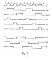
- the circuit to be relayed is a three-phase electronic clock generator, which generates the signals according to FIG. 6 from the input clock signal Q.
- the states desired to be distinguished - as can be seen in FIG. 6 - are provided with the status symbols 0 to 5.
- the state graph to be recorded from this is shown in FIG.
- the number of feedback outputs 12 and address inputs 13 can be determined.
- signals are determined, the number of which corresponds at least to the number of states of the desired sequence controls according to the logarithm on the basis of 2 - the determination is made on the basis of the state graph - after which the signals determined in this way apart from the condition inputs 3 of the Memory 1 can also be fed back to the further address inputs 14.
- the number of feedback outputs 12 is determined in this way.
- the required minimum size of the memory 1 is determined. From the simplicity of the example, it is clear that a 16 x 8 bit memory r is sufficient to solve the task.
- the states not used for the function are then coded. It is useful if the two do not function. used states (101,010) are selected as transition states, from which the system is reset to the stable state 111.
- the contents of the compartment 33 of the accumulator 1 is to be chosen so that at the determined by the feedback outputs QA, QB, QC 12 storage parts, a new forming of the further address inputs 14 Z ustandsein saun dependent condition code is present, while at the non-fed-back outputs Yl-Y5 the code shows corresponding to the desired success signals 4.
- the task consists in determining the content of the memory 1, ie in coding the functions corresponding to the task.
- Figure 9 shows a possible solution to the given task tabulated based on the corresponding code.
Landscapes
- Physics & Mathematics (AREA)
- General Physics & Mathematics (AREA)
- Engineering & Computer Science (AREA)
- Automation & Control Theory (AREA)
- Logic Circuits (AREA)
Applications Claiming Priority (2)
| Application Number | Priority Date | Filing Date | Title |
|---|---|---|---|
| HU471784A HU195344B (en) | 1984-12-19 | 1984-12-19 | Circuit arrangement for forming sequential control circuit |
| HU471784 | 1984-12-19 |
Publications (1)
| Publication Number | Publication Date |
|---|---|
| EP0187985A1 true EP0187985A1 (fr) | 1986-07-23 |
Family
ID=10968751
Family Applications (1)
| Application Number | Title | Priority Date | Filing Date |
|---|---|---|---|
| EP85116280A Withdrawn EP0187985A1 (fr) | 1984-12-19 | 1985-12-19 | Méthode et disposition de circuit pour réaliser un dispositif à commande séquentielle en utilisant une mémoire à boucle fermée |
Country Status (4)
| Country | Link |
|---|---|
| EP (1) | EP0187985A1 (fr) |
| DD (1) | DD243128A5 (fr) |
| HU (1) | HU195344B (fr) |
| PL (1) | PL256937A1 (fr) |
Cited By (4)
| Publication number | Priority date | Publication date | Assignee | Title |
|---|---|---|---|---|
| EP0291615A1 (fr) * | 1987-04-22 | 1988-11-23 | International Business Machines Corporation | Commande séquentielle programmable pour gestion de procédés rapides complexes |
| EP0442580A1 (fr) * | 1990-02-16 | 1991-08-21 | Koninklijke Philips Electronics N.V. | Circuit d'une machine séquentielle à état fini et circuit intégré muni d'un tel circuit |
| EP0400612A3 (fr) * | 1989-06-02 | 1992-07-15 | Hitachi, Ltd. | Automate programmable |
| EP0595707A1 (fr) * | 1992-10-29 | 1994-05-04 | Alcatel Mobile Communication France | Séquenceur linéaire avec signaux de sortie binaires |
-
1984
- 1984-12-19 HU HU471784A patent/HU195344B/hu not_active IP Right Cessation
-
1985
- 1985-12-10 DD DD28405885A patent/DD243128A5/de unknown
- 1985-12-19 EP EP85116280A patent/EP0187985A1/fr not_active Withdrawn
- 1985-12-19 PL PL25693785A patent/PL256937A1/xx unknown
Non-Patent Citations (2)
| Title |
|---|
| ELECTRONIC DESIGN, Band 14, 8. Juli 1971, Seiten 70-71, Rochelle Park, US; W.Z. FLETCHER et al.: "Simplify sequential circuit designs with programmable ROMs" * |
| ELECTRONICS, Band 52, Nr. 8, 12. April 1979, Seiten 134-138, New York, US; J.J. PETRALE: "PROM controller makes fast work of serial jobs" * |
Cited By (7)
| Publication number | Priority date | Publication date | Assignee | Title |
|---|---|---|---|---|
| EP0291615A1 (fr) * | 1987-04-22 | 1988-11-23 | International Business Machines Corporation | Commande séquentielle programmable pour gestion de procédés rapides complexes |
| US4931985A (en) * | 1987-04-22 | 1990-06-05 | International Business Machines Corporation | Programmable sequencing device for controlling fast complex processes |
| EP0400612A3 (fr) * | 1989-06-02 | 1992-07-15 | Hitachi, Ltd. | Automate programmable |
| EP0442580A1 (fr) * | 1990-02-16 | 1991-08-21 | Koninklijke Philips Electronics N.V. | Circuit d'une machine séquentielle à état fini et circuit intégré muni d'un tel circuit |
| EP0595707A1 (fr) * | 1992-10-29 | 1994-05-04 | Alcatel Mobile Communication France | Séquenceur linéaire avec signaux de sortie binaires |
| FR2697650A1 (fr) * | 1992-10-29 | 1994-05-06 | Alcatel Radiotelephone | Programmateur de signaux de sortie binaires. |
| US5584021A (en) * | 1992-10-29 | 1996-12-10 | Alcatel Radiotelephone | Binary output signal programmer using stored start and end location and timing signal states |
Also Published As
| Publication number | Publication date |
|---|---|
| HU195344B (en) | 1988-04-28 |
| PL256937A1 (en) | 1986-11-04 |
| HUT38735A (en) | 1986-06-30 |
| DD243128A5 (de) | 1987-02-18 |
Similar Documents
| Publication | Publication Date | Title |
|---|---|---|
| DE2608902C3 (de) | Code-Wandler-Vorrichtung | |
| DE3818546C2 (fr) | ||
| DE3200894C2 (fr) | ||
| DE1524239A1 (de) | Verfahren zur Lokalisierung eines Fehlers in einer Anlage mit mindestens zwei parallel arbeitenden Rechengeraeten | |
| DE4218787C2 (de) | Selbstschaltende Einrichtung für eine Zentraleinheits-Logik | |
| DE3015992A1 (de) | Programmierbare logische anordnung | |
| DE2646162B2 (de) | Schaltungsanordnung zum Ersetzen fehlerhafter Informationen in Speicherplätzen eines nicht veränderbaren Speichers | |
| DE1280595B (de) | Anordnung zur Loesung eines klammerfreien mathematischen Ausdruckes | |
| DE2854782C2 (de) | Datenverarbeitungssystem und Verfahren zum Ersetzen eines Datenblocks in einem Schnellspeicher | |
| DE2744434A1 (de) | Prozessteuersystem und verfahren zur prozessteuerung | |
| DE3688564T2 (de) | Sequentielle logische Schaltung. | |
| DE2935101C2 (fr) | ||
| DE3529033C2 (fr) | ||
| EP0187985A1 (fr) | Méthode et disposition de circuit pour réaliser un dispositif à commande séquentielle en utilisant une mémoire à boucle fermée | |
| DE69033371T2 (de) | Statusregister für einen Mikroprozessor | |
| DE3743438C2 (de) | Verfahren und Einrichtung zum Erzeugen von Steuersignalen | |
| DE3586789T2 (de) | Mikrocomputer mit wenigstens einer ein-/ausgabeeinheit. | |
| DE2403669A1 (de) | Spezialcomputer | |
| DE69502133T2 (de) | Datenprozessor mit gemeinsamen Anschluss zur Überwachung von internen und externen Speicherereignissen | |
| DE2336143C2 (de) | Logische Schaltung | |
| DE3417816C2 (fr) | ||
| DE1292183B (de) | Schaltungsanordnung zur Phasenkorrektur von von einem Taktgeber abgegebenen Signalen durch impulsfoermige Steuersignale | |
| EP0017245B1 (fr) | Circuit semiconducteur intégré monolithique comportant un registre à décalage commandé par impulsions d'horloge | |
| DE2056981C3 (de) | Hybrid-Rechner | |
| DE3240926C2 (de) | Logikanalysator |
Legal Events
| Date | Code | Title | Description |
|---|---|---|---|
| PUAI | Public reference made under article 153(3) epc to a published international application that has entered the european phase |
Free format text: ORIGINAL CODE: 0009012 |
|
| AK | Designated contracting states |
Kind code of ref document: A1 Designated state(s): AT BE CH DE FR GB IT LI LU NL SE |
|
| 17P | Request for examination filed |
Effective date: 19870115 |
|
| 17Q | First examination report despatched |
Effective date: 19880331 |
|
| STAA | Information on the status of an ep patent application or granted ep patent |
Free format text: STATUS: THE APPLICATION IS DEEMED TO BE WITHDRAWN |
|
| 18D | Application deemed to be withdrawn |
Effective date: 19881111 |
|
| RIN1 | Information on inventor provided before grant (corrected) |
Inventor name: BARTA, PAL, DIPL.-ELEK. Inventor name: HALMI, GABOR, DIPL.-ELEK. Inventor name: VITEZ, GYOERGY |