EP0188329A2 - AM-Signalsender - Google Patents
AM-Signalsender Download PDFInfo
- Publication number
- EP0188329A2 EP0188329A2 EP86300099A EP86300099A EP0188329A2 EP 0188329 A2 EP0188329 A2 EP 0188329A2 EP 86300099 A EP86300099 A EP 86300099A EP 86300099 A EP86300099 A EP 86300099A EP 0188329 A2 EP0188329 A2 EP 0188329A2
- Authority
- EP
- European Patent Office
- Prior art keywords
- pulse width
- voltage
- amplifier
- modulation
- transmitter
- Prior art date
- Legal status (The legal status is an assumption and is not a legal conclusion. Google has not performed a legal analysis and makes no representation as to the accuracy of the status listed.)
- Granted
Links
Images

Classifications
-
- H—ELECTRICITY
- H03—ELECTRONIC CIRCUITRY
- H03F—AMPLIFIERS
- H03F3/00—Amplifiers with only discharge tubes or only semiconductor devices as amplifying elements
- H03F3/20—Power amplifiers, e.g. Class B amplifiers, Class C amplifiers
- H03F3/24—Power amplifiers, e.g. Class B amplifiers, Class C amplifiers of transmitter output stages
Definitions
- the present invention relates to a transmitter for an amplitude modulated signal and more particularly, an AM signal transmitter provided with a pulse width modulation system.
- AM transmitter comprises a modulation amplifier and a modulated power amplifier of the final stage connected in series, the modulation amplifier being subject to pulse operation by a pulse width modulated signal.
- Another prior art AM transmitter is disclosed in UK Patent Application GB 2,079,105, whose modulation amplifier section is structured in a push-pull arrangement.
- the power supply source has to have a voltage about twice that needed for operating the power amplifier of the final stage. Therefore, this leads to disadvantages of a high cost and greater danger derived from the higher voltage.
- An object of the present invention is to provide an AM signal transmitter which does not require a higher power supply source voltage than a voltage for driving the power amplifier circuit at the final stage.
- Another object of the present invention is to provide an AM signal transmitter in which a common power supply source can be used for the modulation amplifier stage and the power amplifier stage, resulting in reduction of a production cost.
- the AM signal transmitter according to the invention is defined in the appended claims.
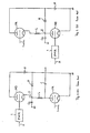
- FIGS. l(a) and l(b) are pulse width modulated transmitters.
- a modulation amplifier MO which is turned on and off by the output of a pulse with modulator 1
- a modulated power amplifier PA which is turned on and off by a high frequency carrier signal
- the anode of the modulation amplifier MO is connected to the positive side of the power supply source V; the cathode thereof is connected to the anode of the modulated amplifier PA through the inductance L; the cathode of the modulated amplifier PA is connected to the negative side (ground) of the power supply source V; and the cathode of the modulation amplifier MO is connected by a diode R to the negative side of the power supply source V.
- the modulated carrier signal is output from the anode of the modulated amplifier PA through a capacitor C.
- the circuit configuration described above is capable of amplitude modulation with a high power and high efficiency by switching on and off the modulation amplifier MO at pulse widths proportional to the amplitudes of a low frequency signal (an audio signal) A and by accumulating energy into the inductance L while the modulation amplifier MO is on.
- this circuit configuration of the prior art has a disadvantage that modulation distortion occurs and the efficiency is lowered, by a stray capacitance C presented between a filament of the modulation amplifier MO, i.e., the point D and ground.
- a greater part of the stray capacitance C s is attributable to the stray capacitance of a filament transformer, and therefore it is difficult to eliminate.
- the power consumed in the modulation amplifier MO corresponds to a carrier component plus a side band component, and therefore it requires a capacity at least equal to that of the modulated power amplifier PA. Furthermore, when the modulation amplifier MO is cut off, the diode R is made conductive, so that the diode should have a enough capacity to withstand the voltage and a peak current, which are applied to the modulation amplifier MO.
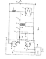
- FI G . 2 is a circuit diagram illustrating one preferred embodiment of the present invention.
- the embodiment comprises a pulse width modulator 1 for modulating a pulse width in accordance with an amplitude of a low frequency signal (an audio signal) A, a modulation amplifier 2 for amplifying the output of the pulse width modulator l, a low pass filter 3 for accumulating the output of the modulation amplifier 2, a low frequency transformer 4 for raising the voltage of the output delivered from the low pass filter 3, and a modulated power amplifier 5 whose driving DC voltage is increased and decreased in response to the output of the low frequency transformer 4.
- this figure contains coupling capacitors 6 and 7, a modulation choke coil 8, and a common power supply source 9.
- the low frequency signal represented by FIG. 3(A) is fed to the pulse width modulator 1.
- Modulated pulse trains B and C are produced by the pulse width modulator 1.
- the pulse train : B consists of pulses having a shorter pitch than the pitch of the highest frequency of the low frequency signal A, and widths corresponds to the instantaneous magnitude of the low frequency signal A. Further, the pulse width reaches its minimum (not zero) for the trough of the low frequency signals A and its maximum (slightly narrower than the pulse pitch), i.e., approximately half the pulse pitch for the peak.
- the pulse train C is reverse to the pulse train B in polarity.
- the pulse width at the trough of the low frequency signal is set to zero and the pulse width at the peak is set to the pulse pitch.
- the non-zero narrow pulse width at the trough of the low frequency signals A and the pulse width slightly narrower than the pulse pitch at the peak are applied.
- switching elements 10 and 11 together constituting a push-pull arrangement, are composed of vacuum tubes or semiconductor elements.
- the switching element 10 is turned on and off in response to the high and low levels of the pulse train B respectively, while the switching element 11 is turned on and off in response to the high and low levels of the pulse train C respectively. Therefore, the switching elements 10 and 11 are turned on and off in a mutually complementary manner.
- the switching element 10 is turned on, the voltage of an output D of the modulation amplifier 2 is slightly lower than the voltage V of the power supply source 9, and when the switching element 11 is turned on, the voltage of the output D is slightly higher than zero. Consequently, the voltage waveform of the output D of the modulation amplifier 2 is such as shown in FIG. 3(D).
- an input voltage waveform to the low frequency transformer 4 becomes as shown in FIG. 3(E), having a peak-to-peak V(1- ⁇ ) AC voltage.
- This is an amplified signal of the low frequency signals A.
- the maximum level of the output waveform at the transformer's secondary winding will be exactly V(2 V peak to peak).
- the voltage-raised output waveform is added to the source voltage V supplied through the modulation choke coil 8 and the added voltage is supplied to the modulated power amplifier 5.
- the added voltage F supplied to the modulated power amplifier 5 varies between 2 V and 0 centering around the source voltage V as shown in FIG. 3(F), when the input low frequency signal A has a magnitude for the maximum modulation. Therefore, in this case, the modulated power amplifier 5 can produce an AM carrier 100% modulated.
- the modulation amplifier 2 since the modulation amplifier 2 does not treat the carrier, its average power consumption is saved, and it is sufficient to use two elements whose capacity is only a.quarter of that of the prior art configuration shown in Figs. l(a) and l(b). Therefore, the transmitter can be readily reduced in dimensions, cost, and the stray capacity.
- the low pass filter 3 In the low pass filter 3, no DC current flows, but only the low frequency signal does. This feature contributes to the reduction of size and cost of the low pass filter 3.
- this embodiment needs no diode for supplying large peak current when the modulation amplifier is cut off.
- the present invention enables an AM transmitter to be operated by a common power supply source having a voltage no more than half that is required in prior art transmitters.
- the present invention can reduce the size and the number of constituent elements in a transmitter.
Landscapes
- Engineering & Computer Science (AREA)
- Power Engineering (AREA)
- Amplifiers (AREA)
- Amplitude Modulation (AREA)
Applications Claiming Priority (2)
| Application Number | Priority Date | Filing Date | Title |
|---|---|---|---|
| JP1956/85 | 1985-01-09 | ||
| JP60001956A JPS61161005A (ja) | 1985-01-09 | 1985-01-09 | 振幅変調送信機 |
Publications (3)
| Publication Number | Publication Date |
|---|---|
| EP0188329A2 true EP0188329A2 (de) | 1986-07-23 |
| EP0188329A3 EP0188329A3 (en) | 1988-01-27 |
| EP0188329B1 EP0188329B1 (de) | 1990-09-05 |
Family
ID=11516046
Family Applications (1)
| Application Number | Title | Priority Date | Filing Date |
|---|---|---|---|
| EP86300099A Expired EP0188329B1 (de) | 1985-01-09 | 1986-01-08 | AM-Signalsender |
Country Status (4)
| Country | Link |
|---|---|
| US (1) | US4723308A (de) |
| EP (1) | EP0188329B1 (de) |
| JP (1) | JPS61161005A (de) |
| DE (1) | DE3673830D1 (de) |
Cited By (1)
| Publication number | Priority date | Publication date | Assignee | Title |
|---|---|---|---|---|
| EP0562255A1 (de) * | 1992-03-27 | 1993-09-29 | Thomcast Ag | Amplitudenmodulierter Rundfunksender für verschiedene Modulationsarten, insbesondere DSB, SSB und ISB |
Families Citing this family (3)
| Publication number | Priority date | Publication date | Assignee | Title |
|---|---|---|---|---|
| US4866737A (en) * | 1987-07-21 | 1989-09-12 | Bruce Seifried | High speed voiceband data transmission and reception |
| US5175877A (en) * | 1990-03-15 | 1992-12-29 | Magnavox Electronic Systems Company | Apparatus and method for generating an amplitude modulated rf signal |
| RU2123760C1 (ru) * | 1994-02-08 | 1998-12-20 | Российский институт мощного радиостроения | Передатчик амплитудно-модулированных сигналов |
Family Cites Families (11)
| Publication number | Priority date | Publication date | Assignee | Title |
|---|---|---|---|---|
| US2235549A (en) * | 1939-12-15 | 1941-03-18 | Gen Electric | Modulator |
| US3413570A (en) * | 1966-02-23 | 1968-11-26 | Collins Radio Co | High efficiency rf power amplification with modulation signal controlled "on"-"off" switch varied amplifier dc potentials |
| US3435378A (en) * | 1966-03-25 | 1969-03-25 | Communications Patents Ltd | Apparatus for generating modulated waves from pulse-type modulating signal |
| US4063199A (en) * | 1977-02-10 | 1977-12-13 | Rca Corporation | Radio frequency pulse width amplitude modulation system |
| US4122415A (en) * | 1977-03-21 | 1978-10-24 | Rca Corporation | AM transmitter with an offset voltage to the RF stage to compensate for switching time of the modulators |
| DE2720930C3 (de) * | 1977-05-10 | 1980-12-11 | Licentia Patent-Verwaltungs-Gmbh, 6000 Frankfurt | Amplitudenmodulierter Sender |
| GB1551711A (en) * | 1978-03-02 | 1979-08-30 | Marconi Ltd | Modulation circuits |
| US4272737A (en) * | 1979-05-25 | 1981-06-09 | The Marconi Company Limited | Pulse width modulator for amplitude modulation circuit |
| GB2079105B (en) * | 1981-02-27 | 1984-07-11 | Marconi Co Ltd | A pulse width modulation system |
| US4336615A (en) * | 1980-10-02 | 1982-06-22 | Rca Corporation | Linear loading for PWM filter |
| CH664655A5 (de) * | 1980-12-12 | 1988-03-15 | Patelhold Patentverwertung | Verfahren und verstaerkerschaltung zum verstaerken elektrischer signale, insbesondere nf-modulationssignale eines rundfunksenders. |
-
1985
- 1985-01-09 JP JP60001956A patent/JPS61161005A/ja active Pending
-
1986
- 1986-01-06 US US06/816,195 patent/US4723308A/en not_active Expired - Fee Related
- 1986-01-08 EP EP86300099A patent/EP0188329B1/de not_active Expired
- 1986-01-08 DE DE8686300099T patent/DE3673830D1/de not_active Expired - Lifetime
Cited By (1)
| Publication number | Priority date | Publication date | Assignee | Title |
|---|---|---|---|---|
| EP0562255A1 (de) * | 1992-03-27 | 1993-09-29 | Thomcast Ag | Amplitudenmodulierter Rundfunksender für verschiedene Modulationsarten, insbesondere DSB, SSB und ISB |
Also Published As
| Publication number | Publication date |
|---|---|
| US4723308A (en) | 1988-02-02 |
| DE3673830D1 (de) | 1990-10-11 |
| EP0188329B1 (de) | 1990-09-05 |
| JPS61161005A (ja) | 1986-07-21 |
| EP0188329A3 (en) | 1988-01-27 |
Similar Documents
| Publication | Publication Date | Title |
|---|---|---|
| US3413570A (en) | High efficiency rf power amplification with modulation signal controlled "on"-"off" switch varied amplifier dc potentials | |
| EP0483094B1 (de) | Pulsbreitenmodulierter linearer Leistungsverstärker | |
| US4164714A (en) | Polyphase PDM amplifier | |
| US4319359A (en) | Radio transmitter energy recovery system | |
| US8004360B2 (en) | Close-loop Class-D audio amplifier and control method thereof | |
| US7321262B2 (en) | Power conversion system | |
| US4752747A (en) | Device for increasing the output power of a low-tension operated radio set, particularly of the car radio set type | |
| USRE40550E1 (en) | Method and device for improved class BD amplification having single-terminal alternating-rail dual-sampling topology | |
| JPH02262705A (ja) | パルス幅変調増幅回路 | |
| US6535399B2 (en) | Tracking power supply controlling | |
| EP0188329B1 (de) | AM-Signalsender | |
| US4122415A (en) | AM transmitter with an offset voltage to the RF stage to compensate for switching time of the modulators | |
| US4369409A (en) | Low-frequency power amplifier | |
| US20020033734A1 (en) | Self-oscillating variable frequency closed loop class d amplifier | |
| EP0236068A2 (de) | AM-RF-Sender mit Kompensation der Änderungen der Stromversorgung | |
| US7279966B2 (en) | Systems for pseudo-BD modulation | |
| US4336615A (en) | Linear loading for PWM filter | |
| ES2081862T3 (es) | Circuito de correccion de acerico lateral modulado por carga de audio. | |
| US20240243704A1 (en) | Self-Oscillating Class D Audio Amplifier With Voltage Limiting Circuit | |
| US3564417A (en) | Single sideband transmission system for producing a maximum amplitude signal | |
| KR100256377B1 (ko) | 저전압 증폭장치 | |
| KR100428241B1 (ko) | 디지털 증폭기 | |
| SU1188852A1 (ru) | Усилитель посто нного тока с гальваническим разделением | |
| RU2007869C1 (ru) | Радиопередатчик с двухтактным модулятором | |
| SU1003328A1 (ru) | Формирователь тока |
Legal Events
| Date | Code | Title | Description |
|---|---|---|---|
| PUAI | Public reference made under article 153(3) epc to a published international application that has entered the european phase |
Free format text: ORIGINAL CODE: 0009012 |
|
| 17P | Request for examination filed |
Effective date: 19860115 |
|
| AK | Designated contracting states |
Kind code of ref document: A2 Designated state(s): CH DE FR GB LI |
|
| PUAL | Search report despatched |
Free format text: ORIGINAL CODE: 0009013 |
|
| AK | Designated contracting states |
Kind code of ref document: A3 Designated state(s): CH DE FR GB LI |
|
| 17Q | First examination report despatched |
Effective date: 19891114 |
|
| GRAA | (expected) grant |
Free format text: ORIGINAL CODE: 0009210 |
|
| AK | Designated contracting states |
Kind code of ref document: B1 Designated state(s): CH DE FR GB LI |
|
| REF | Corresponds to: |
Ref document number: 3673830 Country of ref document: DE Date of ref document: 19901011 |
|
| ET | Fr: translation filed | ||
| PLBE | No opposition filed within time limit |
Free format text: ORIGINAL CODE: 0009261 |
|
| STAA | Information on the status of an ep patent application or granted ep patent |
Free format text: STATUS: NO OPPOSITION FILED WITHIN TIME LIMIT |
|
| 26N | No opposition filed | ||
| PGFP | Annual fee paid to national office [announced via postgrant information from national office to epo] |
Ref country code: GB Payment date: 19911231 Year of fee payment: 7 |
|
| PGFP | Annual fee paid to national office [announced via postgrant information from national office to epo] |
Ref country code: FR Payment date: 19920109 Year of fee payment: 7 |
|
| PGFP | Annual fee paid to national office [announced via postgrant information from national office to epo] |
Ref country code: CH Payment date: 19920129 Year of fee payment: 7 |
|
| PGFP | Annual fee paid to national office [announced via postgrant information from national office to epo] |
Ref country code: DE Payment date: 19920330 Year of fee payment: 7 |
|
| PG25 | Lapsed in a contracting state [announced via postgrant information from national office to epo] |
Ref country code: GB Effective date: 19930108 |
|
| PG25 | Lapsed in a contracting state [announced via postgrant information from national office to epo] |
Ref country code: LI Effective date: 19930131 Ref country code: CH Effective date: 19930131 |
|
| GBPC | Gb: european patent ceased through non-payment of renewal fee |
Effective date: 19930108 |
|
| PG25 | Lapsed in a contracting state [announced via postgrant information from national office to epo] |
Ref country code: FR Effective date: 19930930 |
|
| REG | Reference to a national code |
Ref country code: CH Ref legal event code: PL |
|
| PG25 | Lapsed in a contracting state [announced via postgrant information from national office to epo] |
Ref country code: DE Effective date: 19931001 |
|
| REG | Reference to a national code |
Ref country code: FR Ref legal event code: ST |