EP0188828A2 - Bildverarbeitungsgerät und Interkommunikationsbus dafür - Google Patents
Bildverarbeitungsgerät und Interkommunikationsbus dafür Download PDFInfo
- Publication number
- EP0188828A2 EP0188828A2 EP85201819A EP85201819A EP0188828A2 EP 0188828 A2 EP0188828 A2 EP 0188828A2 EP 85201819 A EP85201819 A EP 85201819A EP 85201819 A EP85201819 A EP 85201819A EP 0188828 A2 EP0188828 A2 EP 0188828A2
- Authority
- EP
- European Patent Office
- Prior art keywords
- data
- bus
- sub
- buses
- address
- Prior art date
- Legal status (The legal status is an assumption and is not a legal conclusion. Google has not performed a legal analysis and makes no representation as to the accuracy of the status listed.)
- Granted
Links
Images


Classifications
-
- G—PHYSICS
- G06—COMPUTING OR CALCULATING; COUNTING
- G06F—ELECTRIC DIGITAL DATA PROCESSING
- G06F13/00—Interconnection of, or transfer of information or other signals between, memories, input/output devices or central processing units
- G06F13/38—Information transfer, e.g. on bus
- G06F13/42—Bus transfer protocol, e.g. handshake; Synchronisation
- G06F13/4204—Bus transfer protocol, e.g. handshake; Synchronisation on a parallel bus
- G06F13/4208—Bus transfer protocol, e.g. handshake; Synchronisation on a parallel bus being a system bus, e.g. VME bus, Futurebus, Multibus
- G06F13/4217—Bus transfer protocol, e.g. handshake; Synchronisation on a parallel bus being a system bus, e.g. VME bus, Futurebus, Multibus with synchronous protocol
-
- G—PHYSICS
- G06—COMPUTING OR CALCULATING; COUNTING
- G06F—ELECTRIC DIGITAL DATA PROCESSING
- G06F13/00—Interconnection of, or transfer of information or other signals between, memories, input/output devices or central processing units
- G06F13/14—Handling requests for interconnection or transfer
- G06F13/36—Handling requests for interconnection or transfer for access to common bus or bus system
- G06F13/368—Handling requests for interconnection or transfer for access to common bus or bus system with decentralised access control
- G06F13/37—Handling requests for interconnection or transfer for access to common bus or bus system with decentralised access control using a physical-position-dependent priority, e.g. daisy chain, round robin or token passing
-
- G—PHYSICS
- G06—COMPUTING OR CALCULATING; COUNTING
- G06T—IMAGE DATA PROCESSING OR GENERATION, IN GENERAL
- G06T1/00—General purpose image data processing
- G06T1/20—Processor architectures; Processor configuration, e.g. pipelining
Definitions
- This invention pertains to the architecture of an image processing apparatus which serves as an intelligent high performance peripheral device in a digital imaging system, such image processing apparatus being recited in the preamble of Claim 1. More specifically, the problems and improvements addressed by the present invention reside in the structure, timing and protocol for use on the bus of such image processing apparatus.
- the bus structure provides an interconnection in which multiple array processors and memory modules can communicate simultaneously at a very high transfer rate for a given number of bus lines and a given clock rate.
- Bus structures for real time video processing to date have a known number of shortcomings.
- a bus architecture must overcome a number of classical drawbacks.
- One common drawback is the inability of the bus structure to achieve maximum throughput because of the inherent time delay between initiation of a memory read cycle and the availability of valid data at the memory output.
- a bus architecture In a multimaster environment, occasionally a very complex arbitration process is needed to satisfy conflicting demands for a bus.
- Many classic designs require very fast memory which in turn increases the cost of a system.
- Interface structures in the prior art have become quite complex because of the timing required for data address and control signals.
- the architecture of the bus structure of the present invention is designed to eliminate the various transmission bottlenecks which have occurred prior art bus designs, such as allowing for a high bit rate, supporting a plurality of master devices being active at the same time, making complex arbitrage operations unnecessary, allowing for a narrow address bus, and in general keeping the apparatus complexity at a low level.
- the object of the invention is realized by the measures recited in the characterizing part of Claim 1. More particularly, in order to keep up with the demands of video rate information transfer, the architecture utilizes a dual bus system. Two sets of buses are defined. One bus is for low speed control and data transfer and the other for the video rate multiple channel image transfer.
- a VME bus is used for the computer controlling functions of the imaging boards and a synchronous video bus is designed to support D data bit lines, which are organized into a plurality of B-bit wide paths.
- the video bus is further decomposed into four functional buses: address selection, data buses, timing and synchronization, and utility and control. This particular distribution of activities removes many bottlenecks and allows for simultaneous image transfers at video rates.
- the invention furthermore relates to an intercommunication bus apparatus for use in an image processing apparatus, featuring the above cited improvements.
- Such bus apparatus can readily be completed by adding necessary modules to function as an image processing apparatus. Further aspects of the invention are recited in dependent Claims.
- the bus structure of the present invention designed for an image processing apparatus, provides for rapid processing of images.
- a typical application is a medical imaging system in which data acquisition, immediate processing and later postprocessing of data from a variety of devices such as CAT scanners, NMR's, radiographic and fluoroscopic instruments is required.
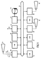
- Figure 1 is a block diagram illustrating the utilization of the bus of the present invention in such a system, in which large arrays of data must pass through various hardware modules very quickly, up to a video rate.
- the bus apparatus has a uniform, nondedicated, bidirectional structure.
- An image processing module must support multiple asynchronous simultaneous processes. This means that multiple independent process masters should be able to control the movement of different data streams at the same time.
- the bus is designed to allow a maximum of 16 simultaneous video processes, each of which is able to transfer data on at least one video data sub-bus. This constitutes a spatial multiplexing of the video data sub-buses. Since it is impractical to implement 16 address buses, one for each possible process, the architecture of this system uses a tine multiplexed video address bus, having 24 lines in the preferred embodiment.
- each video address accesses a 16 pixel packet. This is also convenient for memory design. Although each 16 pixel data transfer takes 16 clock cycles, an address is asserted during only 1 clock cycle. Therefore, 16 pixels of data on each video data bus can be transferred with all 16 possible process masters having asserted their respective video addresses. In the system of the present invention, no bus arbitration is necessary because the throughput of the address bus exactly matches that of the data buses.
- the various process masters are assigned fixed time slots during which to assert the video addresses.
- a video data bus which is initialized for a read or write operation at the beginning of a process will perform the same operation repeatedly, until a whole array is transferred. The only dynamic control is on writing individual words in the packet.
- the memory consists of storage arrays, each of which can be simultaneously accessed through multiple channels. Therefore, in a memory access both the address in the array and the access channel must be specified. The same memory address can be simultaneously accessed by several processes through respective different channels.
- N sub-buses there are 2 timing clocks, 19 video control signals and 34 collision protection signals.
- the allocation of the N sub-buses is executable under software control.
- Each process can be allocated to one or several data sub-buses as required to match its specific data throughput requirements.
- the processes which perform both memory read and memory write operations are allocated to separate read and write buses, thus eliminating the dead time inherent in a read-to-write transition.
- An address receiver usually a memory board, latches the address at the end of the time slot. This concept minimizes the number of lines needed to address data for all of the N data sub-buses.
- Each address accesses N words, which are transferred serially, one word per clock cycle, on the corresponding data sub-bus.
- the N words accessed with one address are called a packet.
- this packet design it takes the same amount of time, N clock cycles, to transfer all data packets as it takes to address all N data buses. This enables full time use of both the address and the data lines with no dead time. Furthermore, the time, N clock cycles, to access each memory module is increased. This permits the use of slower, less expensive memories and/or increased performance via multiple accesses to the memory, multiporting, during a packet time.
- Up to N simultaneous data transfers, read or write can be performed without the need for data or address arbitration. The number of read and write transfers is optimized in N steps to suit a particular application. Data can be fetched and returns to memory in parallel on different sub-buses without the need for local memory. This provides the optimum data path structure for pipeline processors. Data bus lines D can be subdivided into various word sizes in D/N increments.
- the interfacing to the bus is relatively simple.
- the timing is fully synchronous for data, address and control signals.
- Data buses and address time slots are allocated by the system software, thereby eliminating the need for a request/arbitration/grant cycle.
- the timing of data transfers is fixed with respect to each packet clock, thereby eliminating the need for an acknowledge phase.
- FIG. 1 is a block diagram of a digital image processing apparatus showing an environment in which the video bus apparatus of the present invention may be used.
- the central part of the system is the bus 20.
- the detailing of the bus apparatus to the level of bit lines has been omitted for brevity; interfacing to bus bit lines is well known in the art.
- VME bus other bus structures may be used for the inter-station control.
- Element 24 is a quality colour monitor used to display the image as received from the input system, not shown, which is connected to input 22.
- Bidirectional connection 26 is connected to a recorder for storing images as received. This may be a magnetic or optical recorder, write- once or erasable.
- Element 28 is an interface control unit for a picture that is organized as an array for 512 x 512 pixels of 8 or 16 bits each. The pixels may contain intensity and/or colour information, which colour may be natural or false colour.
- Element 30 is a 4 Mbyte matrix memory, that may store completely one picture (each pixel as two bytes). If the data width of a pixel is reduced, this memory may contain more pictures.
- Connection 32 is for attaching a host computer for controlling the respective further stations for executing selected operations on selected pictures. For brevity, the nature of such picture processing is not described further.
- Element 34 is the system controller station for interfacing the host computer to the control part of the system bus. Alternatively, the host computer may also be used for executing certain picture processing operations.
- Element 36 is a high speed special purpose processor, specifically for executing a limited repertoire of picture manipulation algorithms.
- Elements 38, 40, 42 are 1 megabyte random access memories. In comparison with memory 30, they may either be used for storing a 512 x 512 picture of only four bits per pixel, or for storing a smaller picture of more bits per pixel. Still further, they may be used for storing a larger picture (e.g. 1024 x 1024 bits) of only one bit per pixel. Certain techniques have been described to exchange a certain extent pixel definition in the colour/intensity domain versus pixel definition in the spatial domain.
- Element 44 is a storage controller for interfacing work file apparatus 46 to the system bus. The work file apparatus may be used for archival purposes, or for storing indexing and other retrieveal information relating to the pictures stored via connection 26.
- Elements 48, 50 are video controllers for a 1024 x 1024 picture to be displayed on high resolution monitors 52 or 54.
- the display may consist of a single 1024 x 1024 picture, or of multiple pictures side by side of smaller dimensions, together constituting at most a 1 Mpixel image.
- Element 56 is a further station that may have one of several identities, similar to other stations shown. As indicated, the respective stations have a unidirectional or bidirectional connection with the system bus 20.
- the bidirectional connections may operate according to a half-duplex principle on the level of a picture in that a picture is first read from the station and rewritten thereafter. In that case one of the sixteen sub-buses need to be used by the station in question. If the operation is full-duplex on the level of a picture, the traffic in question may use two sub-buses.
- the configuration as shown roughly corresponds to the maximum throughput realizable with sixteen sub-buses.
- the data carries the following signals:
- data is transferred via sixteen 8-bit video data buses:
- the signals are TTL negative-true.
- Transfer addresses are asserted by process masters on the video address bus:
- the 24 video address lines represent the most significant bits of the 28-bit address space. The least significant four bits are not physically implemented because each video address accesses not a word but a 16-word packet. The numeration of the video address lines starting from 4 instead of 0 emphasizes this fact.
- the signals are TTL, negative-true.
- VCHNO 0 Video channel number lines. Together with the VCHNO 1 the address they define the memory board and the channel to which a particular video access request was addressed.
- WEO...WE15 Word write enable one for each data sub-bus. Defines which words transferred on the bus are to be stored (written) in the memory.
- the write enable signals are transferred serially, in parallel with the corresponding data words (in total 19 video control signals).
- VCONO...VCON1 Reserved for future control functions (such as expansion of channels/board).
- the data bus is synchronous. All info signals changes occur after the leading edge of the system clock and are guaranteed to reach the new state 10 ns before the next leading edge of the system clock is received.
- the other timing characteristics of the data bus is the packet organization. All the events are referenced to a 'packet clock", occurring every 16th clock cycle.
- the timing signals associated with the VIDEO BUS are: BSYSCK System clock: Has a frequency of 9.072 MHz for 60 Hz systems and 9.000 MHz for 50 Hz systems. It is an ECL signal distributed via a 50-0hm line terminated at both ends of the line.
- PACKETCK Pacekt clock TTL negative true signal generated once every 16 SYSCK pulses.
- a collision protection mechanism is used. It consists of seventeen daisy chain organizations (one for each video data sub-bus and one more for the video address bus). Each station has up to seventeen "Grant out” connections and as many "Grant in” connections which pairwise correspond to a data/address (sub)bus, and which are daisy chained along the stations. For brevity, no further specifics are given on the priority levels of the respective stations with respect to the respective (sub)-buses.
- Timing of the data bus is governed by 2 periodical signals, the system clock BSYSCK and the packet clock BPACKETCK.
- the duration of a system clock period is also called a time slot.
- the sixteen time slots (between any 2 packet clocks) are labeled from 0 to 15 ( Figure 2). This is an arbitrary notation without any special significance regarding the address or data packets. The important factor is that the address, write data, and read data packets have a fixed timing with respect to the packet clock.
- the address packet starts 2 time slots before the (buffered) packet clock.
- the write data packet starts one time slot after the buffered packet clock.
- the read data packet starts 3 time slots after the buffered packet clock. This is illustrated in Figure 3.
- the data buses and address time slots are dynamically allocated before the transfer by the system software.
- the master station monitors the packet clock and determines the start of an address packet. Then three system clock cycles later, it starts shifting out the data and "write enable" signals to the allocated bus(es). At the same time, the master waits for any (one or more) time slot allocated to it. In each allocated time slot this particular master station may output one address. In the present example only one address is output as indicated by the address validation signal VADDVAL and the cross-hatching of the address signal.
- VADDVAL address validation signal
- the above is the whole write transfer protocol.
- the unusual characteristic of it is the timing of address sending which is decoupled from the start of data transfer. In many instances the address can be validated after the data starts being transferred, as opposed to all "classic" buses where the sequence of arbitration/address/data/ acknowledge is mandatory.
- this data is latched whether it is to be used or not.
- the data enters a shift register (or other buffer device) where it is retained until the destination address arrives. Then the receiving device makes its decision to use or discard the data in the shift register buffer. This decision is made before the end of the packet transfer (note the advance of the address cycle with respect to the data packet by three clock periods).
- the actual implementation of this protocol is simpler than that for the "classic" buses because of the fixed, synchronous nature of the bus and because of the absence of arbitration and acknowledge phases of the transfer cycle.
- the only difference between the read transfer ( Figure 5) and the write transfer is in the time of data transfer.
- the address since the data comes from a slave device (usually the memory), the address has to be asserted first and enough time has to be allowed for the data to be accessed in the pipelined memory.
- the start of the data packet is fixed not with respect to the time slot in which the address was asserted, but with respect to the start of the address packet.
- the address is sent and validated during the address packet which starts at clock period "0" as indicated by the validation signal VADDVAL and the cross-hatching of the address period. In this case, the data starts coaing at clock 37 (or 2 address packets and 5 clocks later).
- the data bus is divided into N sub-buses. This permits an independent path to be allocated for each process, from 1 to N processes. No process arbitration is needed. Each process may be allocated to one or several sub-buses as required to match its specific data throughput requirements.
- the data bus is spatially Multiplexed. Processes which perform both memory read and memory write may be allocated to separate read and write sub-buses, thereby eliminating the dead time inherent in a write-to-read transition.
- the addresses of all data sub-buses are time multiplexed on the address bus. Each sub-bus address is transferred during a different clock cycle or time slot. Typically, the address receiver latches the address at the end of the time slot. This minimizes the number of lines needed to address data for all of the N sub-buses.
- Each address accesses up to N words, which are transferred serially one word per clock cycle on the corresponding data sub-bus.
- the N words accessed with one address are called a packet. It takes the same amount of time, N clock cycles, to transfer all data packets as it takes to address all N data buses. This enables full-time use of both the address and the data lines with no dead times.
Landscapes
- Engineering & Computer Science (AREA)
- Theoretical Computer Science (AREA)
- Physics & Mathematics (AREA)
- General Physics & Mathematics (AREA)
- General Engineering & Computer Science (AREA)
- Bus Control (AREA)
- Small-Scale Networks (AREA)
- Television Systems (AREA)
Applications Claiming Priority (2)
| Application Number | Priority Date | Filing Date | Title |
|---|---|---|---|
| US06/673,960 US4604743A (en) | 1984-11-21 | 1984-11-21 | Bus structure for an image processor |
| US673960 | 1996-07-01 |
Publications (3)
| Publication Number | Publication Date |
|---|---|
| EP0188828A2 true EP0188828A2 (de) | 1986-07-30 |
| EP0188828A3 EP0188828A3 (en) | 1988-12-21 |
| EP0188828B1 EP0188828B1 (de) | 1992-06-17 |
Family
ID=24704787
Family Applications (1)
| Application Number | Title | Priority Date | Filing Date |
|---|---|---|---|
| EP85201819A Expired - Lifetime EP0188828B1 (de) | 1984-11-21 | 1985-11-08 | Bildverarbeitungsgerät und Interkommunikationsbus dafür |
Country Status (5)
| Country | Link |
|---|---|
| US (1) | US4604743A (de) |
| EP (1) | EP0188828B1 (de) |
| JP (1) | JPS61182157A (de) |
| DE (1) | DE3586245T2 (de) |
| IL (1) | IL77084A (de) |
Cited By (11)
| Publication number | Priority date | Publication date | Assignee | Title |
|---|---|---|---|---|
| EP0412657A3 (en) * | 1989-08-09 | 1991-05-29 | Picker International, Inc. | Imaging apparatus and methods |
| EP0365960A3 (de) * | 1988-10-24 | 1992-01-29 | The Walt Disney Company | Rechnergestütztes Verfahren zur Herstellung beweglicher Bilder |
| EP0537898A3 (de) * | 1991-09-16 | 1994-01-19 | Ncr Int Inc | |
| WO1996041274A1 (en) * | 1995-06-07 | 1996-12-19 | Advanced Micro Devices, Inc. | Dynamically reconfigurable data bus |
| US5666545A (en) * | 1991-09-18 | 1997-09-09 | Ncr Corporation | Direct access video bus computer system and method for transferring video information using a dedicated video bus |
| US5764980A (en) * | 1988-10-24 | 1998-06-09 | The Walt Disney Company | Method for coordinating production of an animated feature using a logistics system |
| US5973951A (en) * | 1992-05-19 | 1999-10-26 | Sun Microsystems, Inc. | Single in-line memory module |
| WO2007031912A1 (en) * | 2005-09-14 | 2007-03-22 | Koninklijke Philips Electronics N.V. | Method and system for bus arbitration |
| WO2007005891A3 (en) * | 2005-06-30 | 2007-05-03 | Intel Corp | Micro-tile memory interfaces |
| US8253751B2 (en) | 2005-06-30 | 2012-08-28 | Intel Corporation | Memory controller interface for micro-tiled memory access |
| US8878860B2 (en) | 2006-12-28 | 2014-11-04 | Intel Corporation | Accessing memory using multi-tiling |
Families Citing this family (19)
| Publication number | Priority date | Publication date | Assignee | Title |
|---|---|---|---|---|
| US4941088A (en) * | 1985-02-05 | 1990-07-10 | Digital Equipment Corporation | Split bus multiprocessing system with data transfer between main memory and caches using interleaving of sub-operations on sub-busses |
| US5062076A (en) * | 1985-07-12 | 1991-10-29 | Wang Laboratories, Inc. | Cascadable, high-bandwidth, multi-channel image transfer controller |
| US4838274A (en) * | 1987-09-18 | 1989-06-13 | Air Products And Chemicals, Inc. | Perfluoro-crown ethers in fluorine magnetic resonance imaging |
| JP2665813B2 (ja) * | 1990-02-23 | 1997-10-22 | 三菱電機株式会社 | 記憶制御装置 |
| JPH05205005A (ja) * | 1990-03-30 | 1993-08-13 | Internatl Business Mach Corp <Ibm> | ロジック・シミュレーション・マシン用ホスト・インタフェース |
| US5237567A (en) * | 1990-10-31 | 1993-08-17 | Control Data Systems, Inc. | Processor communication bus |
| FR2669448B1 (fr) * | 1990-11-19 | 1993-01-15 | Bull Sa | Architecture de terminal et circuit de gestion. |
| US5175731A (en) * | 1990-12-11 | 1992-12-29 | International Business Machines Corporation | Arbitration circuit for a multimedia system |
| US5245322A (en) * | 1990-12-11 | 1993-09-14 | International Business Machines Corporation | Bus architecture for a multimedia system |
| US5230041A (en) * | 1990-12-11 | 1993-07-20 | International Business Machines Corporation | Bus interface circuit for a multimedia system |
| CA2055554C (en) * | 1990-12-11 | 1998-04-14 | John Monroe Dinwiddie, Jr. | Multimedia system |
| CA2055296C (en) * | 1990-12-11 | 1995-04-04 | Bruce James Wilkie | Analog image signal processor circuit for a multimedia system |
| US5689657A (en) * | 1991-03-30 | 1997-11-18 | Deutsche Itt Industries Gmbh | Apparatus and methods for bus arbitration in a multimaster system |
| US5446866A (en) * | 1992-01-30 | 1995-08-29 | Apple Computer, Inc. | Architecture for transferring pixel streams, without control information, in a plurality of formats utilizing addressable source and destination channels associated with the source and destination components |
| US5317564A (en) * | 1992-12-30 | 1994-05-31 | Intel Corporation | Merging network for collection of data from multi-computers |
| KR980004067A (ko) * | 1996-06-25 | 1998-03-30 | 김광호 | 멀티프로세서 시스템의 데이터 송수신장치 및 방법 |
| JPH1173258A (ja) * | 1997-08-28 | 1999-03-16 | Toshiba Corp | 低消費電力バス構造及びその制御方法、低消費電力バス構造の合成システム及びその合成方法、携帯情報機器 |
| EP1041490A1 (de) * | 1999-03-31 | 2000-10-04 | Hewlett-Packard Company | Vefahren zur Steigerung der Ein-/Ausgabeleistung eines Rechners |
| CN1129072C (zh) * | 1999-10-27 | 2003-11-26 | 盖内蒂克瓦尔有限公司 | 具有可配置数据/地址通道结构的数据处理系统 |
Family Cites Families (4)
| Publication number | Priority date | Publication date | Assignee | Title |
|---|---|---|---|---|
| NL7806841A (nl) * | 1978-06-26 | 1979-12-28 | Bell Telephone Mfg | Tijdverdelingsmultiplex-communicatiestelsel. |
| FR2458957B1 (fr) * | 1979-06-13 | 1986-02-07 | Telediffusion Fse | Concentrateur teleinformatique pour reseau de transmission et de commutation de donnees par paquets |
| US4535448A (en) * | 1982-12-10 | 1985-08-13 | At&T Bell Laboratories | Dual bus communication system |
| JPS59176838A (ja) * | 1983-03-28 | 1984-10-06 | Dainippon Screen Mfg Co Ltd | 画像演算処理方法 |
-
1984
- 1984-11-21 US US06/673,960 patent/US4604743A/en not_active Expired - Lifetime
-
1985
- 1985-11-08 DE DE8585201819T patent/DE3586245T2/de not_active Expired - Fee Related
- 1985-11-08 EP EP85201819A patent/EP0188828B1/de not_active Expired - Lifetime
- 1985-11-18 IL IL77084A patent/IL77084A/xx not_active IP Right Cessation
- 1985-11-21 JP JP60259921A patent/JPS61182157A/ja active Granted
Cited By (17)
| Publication number | Priority date | Publication date | Assignee | Title |
|---|---|---|---|---|
| US5764980A (en) * | 1988-10-24 | 1998-06-09 | The Walt Disney Company | Method for coordinating production of an animated feature using a logistics system |
| EP0365960A3 (de) * | 1988-10-24 | 1992-01-29 | The Walt Disney Company | Rechnergestütztes Verfahren zur Herstellung beweglicher Bilder |
| US5159551A (en) * | 1989-08-09 | 1992-10-27 | Picker International, Inc. | Prism architecture for ct scanner image reconstruction |
| EP0412657A3 (en) * | 1989-08-09 | 1991-05-29 | Picker International, Inc. | Imaging apparatus and methods |
| EP0537898A3 (de) * | 1991-09-16 | 1994-01-19 | Ncr Int Inc | |
| US5666545A (en) * | 1991-09-18 | 1997-09-09 | Ncr Corporation | Direct access video bus computer system and method for transferring video information using a dedicated video bus |
| US5973951A (en) * | 1992-05-19 | 1999-10-26 | Sun Microsystems, Inc. | Single in-line memory module |
| WO1996041274A1 (en) * | 1995-06-07 | 1996-12-19 | Advanced Micro Devices, Inc. | Dynamically reconfigurable data bus |
| US8200883B2 (en) | 2005-06-30 | 2012-06-12 | Intel Corporation | Micro-tile memory interfaces |
| WO2007005891A3 (en) * | 2005-06-30 | 2007-05-03 | Intel Corp | Micro-tile memory interfaces |
| US8866830B2 (en) | 2005-06-30 | 2014-10-21 | Intel Corporation | Memory controller interface for micro-tiled memory access |
| US8032688B2 (en) | 2005-06-30 | 2011-10-04 | Intel Corporation | Micro-tile memory interfaces |
| US8253751B2 (en) | 2005-06-30 | 2012-08-28 | Intel Corporation | Memory controller interface for micro-tiled memory access |
| WO2007031912A1 (en) * | 2005-09-14 | 2007-03-22 | Koninklijke Philips Electronics N.V. | Method and system for bus arbitration |
| US8041869B2 (en) | 2005-09-14 | 2011-10-18 | Koninklijke Philips Electronics N.V. | Method and system for bus arbitration |
| US7765350B2 (en) | 2005-09-14 | 2010-07-27 | Koninklijke Philips Electronics N.V. | Method and system for bus arbitration |
| US8878860B2 (en) | 2006-12-28 | 2014-11-04 | Intel Corporation | Accessing memory using multi-tiling |
Also Published As
| Publication number | Publication date |
|---|---|
| DE3586245D1 (de) | 1992-07-23 |
| IL77084A0 (en) | 1986-04-29 |
| DE3586245T2 (de) | 1993-01-14 |
| EP0188828A3 (en) | 1988-12-21 |
| JPH0555907B2 (de) | 1993-08-18 |
| IL77084A (en) | 1989-10-31 |
| US4604743A (en) | 1986-08-05 |
| JPS61182157A (ja) | 1986-08-14 |
| EP0188828B1 (de) | 1992-06-17 |
Similar Documents
| Publication | Publication Date | Title |
|---|---|---|
| EP0188828B1 (de) | Bildverarbeitungsgerät und Interkommunikationsbus dafür | |
| US4933846A (en) | Network communications adapter with dual interleaved memory banks servicing multiple processors | |
| US4858107A (en) | Computer device display system using conditionally asynchronous memory accessing by video display controller | |
| EP0156580B1 (de) | Datenübertragungssystem | |
| US6072796A (en) | Apparatus and method for accessing memory in a TDM network | |
| US5058051A (en) | Address register processor system | |
| JP3241045B2 (ja) | マルチポート共有メモリインタフェースおよび関連の方法 | |
| US4688168A (en) | High speed data transfer method and apparatus | |
| US6035360A (en) | Multi-port SRAM access control using time division multiplexed arbitration | |
| US5842025A (en) | Arbitration methods and apparatus | |
| US5875309A (en) | Arbitration system using linked table | |
| EP0458926B1 (de) | Zwei toren, zwei geschwindigkeiten-bildspeicherzugriffsanordnung | |
| KR950010458B1 (ko) | 디지탈 데이타 메모리 시스템 | |
| EP0817090A2 (de) | System zur Mehrbreitenbuskopplung in einem paketvermittelten Computersystem | |
| US6920510B2 (en) | Time sharing a single port memory among a plurality of ports | |
| US5625796A (en) | Method and apparatus for concurrently accessing multiple memories with different timing requirements | |
| HK203096A (en) | Apparatus for conditioning priority arbitration in buffered direct memory addressing | |
| US6119188A (en) | Priority allocation in a bus interconnected discrete and/or integrated digital multi-module system | |
| EP0870303A1 (de) | System, architektur und verfahren mit hoher leistung für universeller multiport dynamischer direktzugriffspeicher mit internem cache-speicher | |
| US5566177A (en) | Priority-based arbitrator on a token-based communication medium | |
| JPH0827773B2 (ja) | データ経路を使用可能にする方法、装置およびデータ処理システム | |
| US4849965A (en) | Asynchronous digital time-division multiplexing system with distributed bus | |
| GB2123189A (en) | Communication between computers | |
| US5708850A (en) | Parallel processing system for time division multiplex data transfer including read/write dual port memory accessible to bus and digital signal processor during opposite phases of clock | |
| JP3107650B2 (ja) | タイムスロット割当て装置 |
Legal Events
| Date | Code | Title | Description |
|---|---|---|---|
| PUAI | Public reference made under article 153(3) epc to a published international application that has entered the european phase |
Free format text: ORIGINAL CODE: 0009012 |
|
| AK | Designated contracting states |
Kind code of ref document: A2 Designated state(s): DE FR GB NL |
|
| PUAL | Search report despatched |
Free format text: ORIGINAL CODE: 0009013 |
|
| AK | Designated contracting states |
Kind code of ref document: A3 Designated state(s): DE FR GB NL |
|
| 17P | Request for examination filed |
Effective date: 19890608 |
|
| 17Q | First examination report despatched |
Effective date: 19901114 |
|
| GRAA | (expected) grant |
Free format text: ORIGINAL CODE: 0009210 |
|
| AK | Designated contracting states |
Kind code of ref document: B1 Designated state(s): DE FR GB NL |
|
| PG25 | Lapsed in a contracting state [announced via postgrant information from national office to epo] |
Ref country code: NL Effective date: 19920617 |
|
| REF | Corresponds to: |
Ref document number: 3586245 Country of ref document: DE Date of ref document: 19920723 |
|
| ET | Fr: translation filed | ||
| NLV1 | Nl: lapsed or annulled due to failure to fulfill the requirements of art. 29p and 29m of the patents act | ||
| PLBE | No opposition filed within time limit |
Free format text: ORIGINAL CODE: 0009261 |
|
| STAA | Information on the status of an ep patent application or granted ep patent |
Free format text: STATUS: NO OPPOSITION FILED WITHIN TIME LIMIT |
|
| 26N | No opposition filed | ||
| REG | Reference to a national code |
Ref country code: FR Ref legal event code: CD |
|
| PGFP | Annual fee paid to national office [announced via postgrant information from national office to epo] |
Ref country code: FR Payment date: 19981117 Year of fee payment: 14 |
|
| PGFP | Annual fee paid to national office [announced via postgrant information from national office to epo] |
Ref country code: GB Payment date: 19981123 Year of fee payment: 14 |
|
| PGFP | Annual fee paid to national office [announced via postgrant information from national office to epo] |
Ref country code: DE Payment date: 19990125 Year of fee payment: 14 |
|
| PG25 | Lapsed in a contracting state [announced via postgrant information from national office to epo] |
Ref country code: GB Free format text: LAPSE BECAUSE OF NON-PAYMENT OF DUE FEES Effective date: 19991108 |
|
| GBPC | Gb: european patent ceased through non-payment of renewal fee |
Effective date: 19991108 |
|
| PG25 | Lapsed in a contracting state [announced via postgrant information from national office to epo] |
Ref country code: FR Free format text: LAPSE BECAUSE OF NON-PAYMENT OF DUE FEES Effective date: 20000731 |
|
| PG25 | Lapsed in a contracting state [announced via postgrant information from national office to epo] |
Ref country code: DE Free format text: LAPSE BECAUSE OF NON-PAYMENT OF DUE FEES Effective date: 20000901 |
|
| REG | Reference to a national code |
Ref country code: FR Ref legal event code: ST |