EP0189123A2 - Filtre à ondes acoustiques de surface - Google Patents
Filtre à ondes acoustiques de surface Download PDFInfo
- Publication number
- EP0189123A2 EP0189123A2 EP86100516A EP86100516A EP0189123A2 EP 0189123 A2 EP0189123 A2 EP 0189123A2 EP 86100516 A EP86100516 A EP 86100516A EP 86100516 A EP86100516 A EP 86100516A EP 0189123 A2 EP0189123 A2 EP 0189123A2
- Authority
- EP
- European Patent Office
- Prior art keywords
- additional
- filter
- reflector structure
- adjacent
- reflector
- Prior art date
- Legal status (The legal status is an assumption and is not a legal conclusion. Google has not performed a legal analysis and makes no representation as to the accuracy of the status listed.)
- Granted
Links
Images

Classifications
-
- H—ELECTRICITY
- H03—ELECTRONIC CIRCUITRY
- H03H—IMPEDANCE NETWORKS, e.g. RESONANT CIRCUITS; RESONATORS
- H03H9/00—Networks comprising electromechanical or electro-acoustic elements; Electromechanical resonators
- H03H9/02—Details
- H03H9/02535—Details of surface acoustic wave devices
- H03H9/02637—Details concerning reflective or coupling arrays
-
- H—ELECTRICITY
- H03—ELECTRONIC CIRCUITRY
- H03H—IMPEDANCE NETWORKS, e.g. RESONANT CIRCUITS; RESONATORS
- H03H9/00—Networks comprising electromechanical or electro-acoustic elements; Electromechanical resonators
- H03H9/02—Details
- H03H9/02535—Details of surface acoustic wave devices
- H03H9/02992—Details of bus bars, contact pads or other electrical connections for finger electrodes
-
- Y—GENERAL TAGGING OF NEW TECHNOLOGICAL DEVELOPMENTS; GENERAL TAGGING OF CROSS-SECTIONAL TECHNOLOGIES SPANNING OVER SEVERAL SECTIONS OF THE IPC; TECHNICAL SUBJECTS COVERED BY FORMER USPC CROSS-REFERENCE ART COLLECTIONS [XRACs] AND DIGESTS
- Y10—TECHNICAL SUBJECTS COVERED BY FORMER USPC
- Y10T—TECHNICAL SUBJECTS COVERED BY FORMER US CLASSIFICATION
- Y10T29/00—Metal working
- Y10T29/42—Piezoelectric device making
Definitions
- the present invention relates to an improvement for the structure of a filter which works with acoustic waves running close to the surface in a substrate, as specified in the preamble of patent claim 1.
- a filter relating to the invention can be operated not only with acoustic surface waves (Rayleigh and Bleustein waves) in the narrow sense, but also with Lamb waves, Love waves, surface skimming bulk waves and the like Run substrate at least close to the surface. Which type of wave is generated in the individual case depends on the dimensions of the transducers known to the person skilled in the art and possibly also on the anisotropy properties of the substrate.
- acoustic surface waves Rayleigh and Bleustein waves
- Lamb waves, Love waves, surface skimming bulk waves and the like Run substrate at least close to the surface. Which type of wave is generated in the individual case depends on the dimensions of the transducers known to the person skilled in the art and possibly also on the anisotropy properties of the substrate.
- Surface wave resonator filters in the sense of the invention have digital structures arranged on a piezoelectric substrate, which include interdigital structures and reflector structures to be used as transducers.
- Interdigital structures consist of strip electrodes that are alternately electrically connected or connected to one another.
- the digital structure of a reflector consists of strip-shaped fingers, finger pieces, dots or the like, which are preferably metallization strips applied to the substrate surface.
- Bus bars are provided for interdigital structures, with which the fingers of the one finger structure are connected to one another.
- One finger structure engages with these fingers like a comb into a corresponding second finger structure and together forms the interdigital structure.
- This busbar which is arranged on the side of the interdigital structure, is followed by a (connection) pad which is usually relatively large in area.
- the lead wires required for the interdigital structure used as transducers are connected to these pads, which are connected to the respective busbar or form a part thereof.
- Busbars on reflector structures are given in U.S. Patent 4,454,488, U.S. Patent 4,425,554, U.S. Patent 4,340,834.
- the quality and performance of such a surface wave filter depends, among other things, on the exact design, positioning and precise sharp-edged delimitation of the strip-shaped fingers of the respective one Digital structure, be it that it is an interdigital structure or a reflector structure.
- the present invention is based on the knowledge that the above-mentioned defects of a structure or the structures of a surface acoustic wave filter are based on causes which are related to the photolithographic production and in particular in connection with the projection exposure of the photosensitive layer located on the substrate surface.
- the scope for the exposure intensity of the photosensitive layer material that is still available to sufficiently sharp contours of the strip-shaped fingers to be produced or coatings on the substrate surface in the photolithographic process is relatively narrow. As has been established, it is not sufficient to select exposure intensity and exposure duration that are matched to one another in order to expose all parts of the structures to be produced equally satisfactorily.
- the invention now provides, as will become apparent from the detailed description below, to arrange additional assignments on both sides of a reflector structure, such an additional assignment addressing a continuation of a pad of the adjacent transducer structure extending in the longitudinal direction of the filter and accompanying the reflector structure laterally is.
- additional assignments are dimensioned such that they extend over the entire reflector structure.
- the areas of the accompanying additional assignments provide the same overexposure in the area of the strip-type assignments to be exposed as is the case for a transducer structure provided with pads. It can be seen from this that the width (b) of such an additional assignment should be as large as possible as the width of the adjacent pad in question.
- FIG. 1 shows the structure of a surface acoustic wave filter, this structure comprising alternative configurations which also belong to the invention.
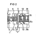
- Figure 2 shows a further variant.
- FIG. 1 designates a surface wave filter relating to the invention, the structure of which is located on the surface of a substrate 2 which is only partially shown, again partially.
- 3 and 4 each have a converter, namely an interdigital structure records, one of which serves as an input converter and the other as an output converter.
- the strip-like assignments also referred to as fingers, digit strips and the like, are designated by 5.
- these strip-shaped coverings 5 are alternately electrically connected to a respective busbar 6.
- these busbars 6 are portions of the pads 7, 7a.
- the supply lines of the relevant transducer connected to the pads 7, 7a are designated by 8.
- the areal continuations of the pads 7, 7a provided according to the invention are designated by 9, 9a.
- the area designated 9 is the continuation of the pad 7 and the area labeled 9a. marked area the continuation of pad 7a.
- overexposure occurs practically equally in a corresponding manner also for the strip-shaped coatings 21 of the reflector structure 20 shown.
- this overexposure emanates from the surfaces of the continuations 9 and 9a.
- the specific area portions of these extensions 9 and 9a are dimensioned at least approximately the same size as the specific area portions of the pads 7 and 7a:
- the term "specific" refers to the longitudinal direction or running direction of the filter 1 indicated by the arrow 100.
- the strip-shaped coverings 21 of the digital structure 20 which acts as a resonator have no busbars, as is also not necessary for a reflector structure.
- the areal extensions 9 and 9a provided according to the invention do not extend to the extreme end of the reflector structure 20 shown.
- the strip-like coatings have at the end opposite the point of incidence of the shaft of the reflector structure 20 are present, in any case only a comparatively much smaller influence on the overall reflection of the structure 20. Therefore, deviations in the positioning and edge definition of such strip-like coatings 21 that are present at the end of the reflector structure 20 from the achievable precision are already negligible influence.
- these extensions 9, 9a will extend to the extreme end of the respective reflector structure, which these extensions 9, 9a Accompany 9a, let go.
- the digital structures of a resonator filter as shown are generally arranged at least essentially symmetrically.
- the right half of the filter 1 in the figure
- the following description relates to a variation within the scope of the invention, this variation of the right half in turn also being able to fill the left half of the filter identically.
- symmetry is not necessary, and also not for a filter according to the invention.
- the pads of the interdigital structure 4 are designated by 17 and 17a. Otherwise, the structure of FIG. 3 above applies at least to this structure.
- resonator structure which has the strip-like coatings 41.
- 19 and 19a designate, area-like continuations of the pads 17 and 17a, respectively. These continuations 19, 19a differ from the continuations 9 and 9a in that they reach as far as the strip-like coverings (fingers, digit strips) 41 of the reflector structure 40 and can even have electrical contact therewith.
- the extensions 19 and 19a provided according to the invention differ from busbars 16, 16a of a reflector structure which are already known to be used in individual cases, above all in their considerably larger width d, namely in their pads 17, 17a correspondingly substantially the same width b.
- the electrical interruption 122 is required so that short circuit between the converter 4 and the reflector structure 40 is excluded.
- the interruptions 122 per se corresponding to the interruptions 22 are, as shown, arranged obliquely.
- This oblique arrangement is particularly advantageous within the scope of the invention if there is no or only a comparatively small distance between the transducer structure 4 and the subsequent reflector structure 40 or this interruption (s) 122 is already positioned laterally next to the reflector structure.
- a transducer structure 3, 4 has e.g. ten to 400, preferably 50 to 150, strip-shaped occupancies in an interdigital arrangement.
- a reflector structure 20, 40 has e.g. 200 to 1000, preferably 400 to 700, strip-like coverings.
- the respective number of strip-shaped occupancies of a transducer or reflector structure depends on each because of the given bandwidth.
- the width and (center) distance of the strip-like coatings from one another is given by the predetermined frequency or wavelength of the acoustic wave and the wave propagation speed in the substrate body. Typical values for the strip width are 0.5 to 5 ⁇ m and for the center distance 1 to 10 ⁇ m.
- the length of the individual strip-shaped coverings is usually between 20 and 200 wavelengths.
- the width b of a pad 7, 7a, 17, 17a and thus also the continuations 9, 9a; 19, 19a is between 10 and 300 ⁇ m.
- the usual width of a busbar 6 is given, which is usually between 1 and 10 .mu.m, that is, that a busbar is extremely narrow compared to the width dimension b of a pad, so that it is readily apparent what a pad and what is only one Busbar is.
- This technique takes into account the production of the digital structures according to the principle of the lift-off technique.
- This technique uses (positive) photosensitive varnish. A coating of the entire surface with such photoresist is first carried out on the substrate surface. The exposure corresponding to the desired structures then takes place, specifically those portions of the surface of the layer located on the substrate surface that are later strip-shaped coatings 5, 21, 41, pads 7, 7a; 17, 17a, busbars and the additional assignments 9, 9a; 19, 19a. After development, the exposed portion of the photoresist is removed loosened and the entire surface (exposed parts of the surface of the substrate surface and remaining photoresist) covered with a metal layer (vaporized). Finally, the areas of the photoresist that are still left are removed, the portions that are on the photoresist are lifted off the metal layer, and the desired structures remain as metallic coatings on the substrate surface.
- the opposite process, so to speak, is the manufacture of the structures (with the same end result) according to a principle of etching technology.
- the substrate surface is first covered with a metal layer.
- This metal layer is coated with the photoresist layer and the exposure now takes place, but here those areas that are free of metallizations of the substrate surface in the finished filter.
- the exposed photoresist has been developed, detachment takes place, the underlying metallization layer on the substrate surface being exposed in the areas which in the finished filter must be free of metallization of the substrate surface.
- Subsequent etching removes these exposed portions of the metallization layer from the substrate surface and the portions of the original metallization of the substrate surface which are protected by the remaining surface portions of the photoresist layer remain as desired structures of the filter during the etching.
- the lifting technique and the etching technique differ in that the complementary areas are exposed.
- the radiation from the pads and from the invention takes place. seen additional assignments.
- the etching technique if the measure according to the invention of the additional assignments has not been made, overexposure takes place in the region of a reflector structure which has no pads.
- the exposure (including the overexposure) to the for the reflector structure 20, 40 in the process of the etching technique, and without additional assignments 9, 9a; 19, 19a are provided, suitable dimensions would be matched, there would be underexposure in the area of the interdigital structures 3, 4, because there is no overexposure in the exposure scheme corresponding to the etching technique because of the pads present.
- FIG. 2 shows a further variant of an embodiment of the invention. Details of FIG. 2 provided with reference numerals from FIG. 1 are identical. There is in each case an electrical interruption-causing gap 216, 216a between the busbar 16, 16a and the additional assignment 219, 219a provided according to the invention.
- the width b 'of the additional assignment 219, 219a is preferably dimensioned such that, together with the width of the respective busbar 16, 16a, the width b (the additional assignment 19 or 19a) results; because the gap 216,
- the electrical interruptions 22, 122 are preferably even so narrow (a possible reduction of the effect aimed for and achieved with the invention is minimized by these interruptions) that these interruptions are practically no longer clearly recognizable in the microscope.
- an additional recess as shown as an example to the interruptions 22, 122 in Figure 1 and with 1022, 1122 are designated.
- These additional recesses 1022, 1122 are preferably dimensioned only to a maximum of approximately b / 4 deep and extend from the outer edge into the respective pad 17, 17a and / or 7, 7a or into the additional assignment 9, 9a. These additional recesses can be clearly seen in the microscope.
Landscapes
- Physics & Mathematics (AREA)
- Acoustics & Sound (AREA)
- Surface Acoustic Wave Elements And Circuit Networks Thereof (AREA)
- Filtering Of Dispersed Particles In Gases (AREA)
- Filtering Materials (AREA)
- Electrical Discharge Machining, Electrochemical Machining, And Combined Machining (AREA)
- Filters And Equalizers (AREA)
- Transplanting Machines (AREA)
Priority Applications (1)
| Application Number | Priority Date | Filing Date | Title |
|---|---|---|---|
| AT86100516T ATE64502T1 (de) | 1985-01-18 | 1986-01-16 | Mit akustischen wellen arbeitendes filter. |
Applications Claiming Priority (2)
| Application Number | Priority Date | Filing Date | Title |
|---|---|---|---|
| DE3501567 | 1985-01-18 | ||
| DE3501567 | 1985-01-18 |
Publications (3)
| Publication Number | Publication Date |
|---|---|
| EP0189123A2 true EP0189123A2 (fr) | 1986-07-30 |
| EP0189123A3 EP0189123A3 (en) | 1988-09-07 |
| EP0189123B1 EP0189123B1 (fr) | 1991-06-12 |
Family
ID=6260158
Family Applications (1)
| Application Number | Title | Priority Date | Filing Date |
|---|---|---|---|
| EP86100516A Expired - Lifetime EP0189123B1 (fr) | 1985-01-18 | 1986-01-16 | Filtre à ondes acoustiques de surface |
Country Status (7)
| Country | Link |
|---|---|
| US (1) | US4682130A (fr) |
| EP (1) | EP0189123B1 (fr) |
| JP (1) | JPS61170111A (fr) |
| AT (1) | ATE64502T1 (fr) |
| CA (1) | CA1246166A (fr) |
| DE (1) | DE3679679D1 (fr) |
| NO (1) | NO855284L (fr) |
Families Citing this family (5)
| Publication number | Priority date | Publication date | Assignee | Title |
|---|---|---|---|---|
| US5133990A (en) * | 1990-04-05 | 1992-07-28 | Crystal Technology, Inc. | Technique for mass production of coded surface acoustic wave devices |
| DE4447741B4 (de) * | 1993-09-06 | 2004-02-05 | Sanyo Electric Co., Ltd., Moriguchi | Akustisches Oberflächenwellenfilter |
| WO1996015587A1 (fr) * | 1994-11-10 | 1996-05-23 | Fujitsu Limited | Filtre a ondes acoustiques |
| JP2002237736A (ja) * | 2001-02-13 | 2002-08-23 | Murata Mfg Co Ltd | 弾性表面波装置及びその弾性表面波装置の周波数調整方法 |
| CN115833770A (zh) * | 2022-12-16 | 2023-03-21 | 深圳飞骧科技股份有限公司 | 声表面波滤波器的制造方法及声表面波滤波器 |
Family Cites Families (5)
| Publication number | Priority date | Publication date | Assignee | Title |
|---|---|---|---|---|
| US4130813A (en) * | 1977-05-23 | 1978-12-19 | Raytheon Company | Surface wave device having enhanced reflectivity gratings |
| DE2909705C2 (de) * | 1979-03-12 | 1984-09-06 | Siemens AG, 1000 Berlin und 8000 München | Akustische Oberflächenwellenanordnung |
| US4354166A (en) * | 1980-10-23 | 1982-10-12 | United Technologies Corporation | Carrier concentration controlled surface acoustic wave resonator and oscillator |
| JPS5936409A (ja) * | 1982-08-25 | 1984-02-28 | Hitachi Ltd | 弾性表面波フイルタの電極幅測定方法 |
| DE3314725A1 (de) * | 1983-04-22 | 1984-10-25 | Siemens AG, 1000 Berlin und 8000 München | Oberflaechenwellen-resonatorfilter |
-
1985
- 1985-12-23 NO NO855284A patent/NO855284L/no unknown
- 1985-12-27 US US06/813,827 patent/US4682130A/en not_active Expired - Fee Related
-
1986
- 1986-01-16 CA CA000499667A patent/CA1246166A/fr not_active Expired
- 1986-01-16 DE DE8686100516T patent/DE3679679D1/de not_active Expired - Lifetime
- 1986-01-16 JP JP61007143A patent/JPS61170111A/ja active Pending
- 1986-01-16 EP EP86100516A patent/EP0189123B1/fr not_active Expired - Lifetime
- 1986-01-16 AT AT86100516T patent/ATE64502T1/de not_active IP Right Cessation
Also Published As
| Publication number | Publication date |
|---|---|
| CA1246166A (fr) | 1988-12-06 |
| ATE64502T1 (de) | 1991-06-15 |
| DE3679679D1 (de) | 1991-07-18 |
| EP0189123B1 (fr) | 1991-06-12 |
| NO855284L (no) | 1986-07-21 |
| US4682130A (en) | 1987-07-21 |
| JPS61170111A (ja) | 1986-07-31 |
| EP0189123A3 (en) | 1988-09-07 |
Similar Documents
| Publication | Publication Date | Title |
|---|---|---|
| DE3942623C2 (fr) | ||
| DE10207329B4 (de) | Verfahren zur Massenbelastung akustischer Dünnfilmvolumenresonatoren (FBARs) zum Erzeugen von Resonatoren mit unterschiedlichen Frequenzen und Vorrichtung, die das Verfahren beinhaltet | |
| DE2821791C2 (fr) | ||
| DE3304053C2 (fr) | ||
| DE10112596C2 (de) | Verfahren zum Herstellen von Oberflächenwellenvorrichtungen | |
| EP1125364B1 (fr) | Systeme a ondes de surface presentant au moins deux structures a ondes de surface | |
| DE10207330B4 (de) | Verfahren zum Herstellen akustischer Dünnfilmvolumenresonatoren (FBARs) mit unterschiedlichen Frequenzen auf dem gleichen Substrat durch ein Subtraktionsverfahren und Vorrichtung, die das Verfahren beinhaltet | |
| DE10207324B4 (de) | Verfahren zum Herstellen akustischer Dünnfilmvolumenresonatoren (FBARs) mit unterschiedlichen Frequenzen auf dem gleichen Substrat durch ein Substraktionsverfahren und Vorrichtung, die das Verfahren beinhaltet | |
| DE10207341B4 (de) | Verfahren zum Erzeugen akustischer Dünnfilmvolumenresonatoren (FBARs) mit unterschiedlichen Frequenzen auf einem einzelnen Substrat und Vorrichtung, die das Verfahren beinhaltet | |
| DE10207342B4 (de) | Verfahren zum Liefern unterschiedlicher Frequenzeinstellungen bei einem akustischen Dünnfilmvolumenresonator- (FBAR-) Filter und Vorrichtung, die das Verfahren beinhaltet | |
| DE68918372T2 (de) | Piezoelektrischer Wandler zur Volumenwellenerregung. | |
| DE3245658C2 (fr) | ||
| DE2521290A1 (de) | Oberflaechenwellenresonatorvorrichtung | |
| DE69321799T2 (de) | Akustische Oberflächenwellenanordnung | |
| DE10207328A1 (de) | Verfahren zum Liefern unterschiedlicher Frequenzeinstellungen bei einem akustischen Dünnfilmvolumenresonator- (FBAR-) Filter und Vorrichtung, die das Verfahren beinhaltet | |
| DE2604105A1 (de) | Oberflaechenwellenbauelement | |
| DE2848267C3 (de) | Akustische Oberflachenwelleneinrichtung | |
| DE4005184C2 (fr) | ||
| DE10138080A1 (de) | Mikrostellgliedvorrichtung, Kopftraganordnung und Plattenaufzeichnungsgerät | |
| DE10241981B4 (de) | Oberflächenwellenbauelement vom Kantenreflexionstyp und Verfahren zum Herstellen desselben | |
| EP0189123B1 (fr) | Filtre à ondes acoustiques de surface | |
| DE10158109A1 (de) | Piezoelektrischer Filter mit mehreren gekoppelten longitudinalen Moden | |
| DE10100833B4 (de) | Piezoelektrischer Resonator | |
| DE2831584A1 (de) | Wandler fuer akustische oberflaechenwellen und filter, ausgefuehrt auf der basis dieses wandlers | |
| DE10117291B4 (de) | Variabler Induktor |
Legal Events
| Date | Code | Title | Description |
|---|---|---|---|
| PUAI | Public reference made under article 153(3) epc to a published international application that has entered the european phase |
Free format text: ORIGINAL CODE: 0009012 |
|
| AK | Designated contracting states |
Kind code of ref document: A2 Designated state(s): AT DE FR GB IT NL |
|
| PUAL | Search report despatched |
Free format text: ORIGINAL CODE: 0009013 |
|
| AK | Designated contracting states |
Kind code of ref document: A3 Designated state(s): AT DE FR GB IT NL |
|
| 17P | Request for examination filed |
Effective date: 19890302 |
|
| 17Q | First examination report despatched |
Effective date: 19900907 |
|
| GRAA | (expected) grant |
Free format text: ORIGINAL CODE: 0009210 |
|
| AK | Designated contracting states |
Kind code of ref document: B1 Designated state(s): AT DE FR GB IT NL |
|
| REF | Corresponds to: |
Ref document number: 64502 Country of ref document: AT Date of ref document: 19910615 Kind code of ref document: T |
|
| REF | Corresponds to: |
Ref document number: 3679679 Country of ref document: DE Date of ref document: 19910718 |
|
| ET | Fr: translation filed | ||
| ITF | It: translation for a ep patent filed | ||
| GBT | Gb: translation of ep patent filed (gb section 77(6)(a)/1977) | ||
| PGFP | Annual fee paid to national office [announced via postgrant information from national office to epo] |
Ref country code: GB Payment date: 19911217 Year of fee payment: 7 |
|
| PGFP | Annual fee paid to national office [announced via postgrant information from national office to epo] |
Ref country code: AT Payment date: 19911231 Year of fee payment: 7 |
|
| PGFP | Annual fee paid to national office [announced via postgrant information from national office to epo] |
Ref country code: FR Payment date: 19920122 Year of fee payment: 7 |
|
| PGFP | Annual fee paid to national office [announced via postgrant information from national office to epo] |
Ref country code: NL Payment date: 19920131 Year of fee payment: 7 |
|
| PLBE | No opposition filed within time limit |
Free format text: ORIGINAL CODE: 0009261 |
|
| STAA | Information on the status of an ep patent application or granted ep patent |
Free format text: STATUS: NO OPPOSITION FILED WITHIN TIME LIMIT |
|
| 26N | No opposition filed | ||
| PG25 | Lapsed in a contracting state [announced via postgrant information from national office to epo] |
Ref country code: GB Effective date: 19930116 Ref country code: AT Effective date: 19930116 |
|
| PG25 | Lapsed in a contracting state [announced via postgrant information from national office to epo] |
Ref country code: NL Effective date: 19930801 |
|
| GBPC | Gb: european patent ceased through non-payment of renewal fee |
Effective date: 19930116 |
|
| NLV4 | Nl: lapsed or anulled due to non-payment of the annual fee | ||
| PG25 | Lapsed in a contracting state [announced via postgrant information from national office to epo] |
Ref country code: FR Effective date: 19930930 |
|
| REG | Reference to a national code |
Ref country code: FR Ref legal event code: ST |
|
| PGFP | Annual fee paid to national office [announced via postgrant information from national office to epo] |
Ref country code: DE Payment date: 20030131 Year of fee payment: 18 |
|
| PG25 | Lapsed in a contracting state [announced via postgrant information from national office to epo] |
Ref country code: DE Free format text: LAPSE BECAUSE OF NON-PAYMENT OF DUE FEES Effective date: 20040803 |
|
| PG25 | Lapsed in a contracting state [announced via postgrant information from national office to epo] |
Ref country code: IT Free format text: LAPSE BECAUSE OF NON-PAYMENT OF DUE FEES;WARNING: LAPSES OF ITALIAN PATENTS WITH EFFECTIVE DATE BEFORE 2007 MAY HAVE OCCURRED AT ANY TIME BEFORE 2007. THE CORRECT EFFECTIVE DATE MAY BE DIFFERENT FROM THE ONE RECORDED. Effective date: 20050116 |