EP0189598A1 - Procédé de fabrication d'un dispositif semi-conducteur - Google Patents
Procédé de fabrication d'un dispositif semi-conducteur Download PDFInfo
- Publication number
- EP0189598A1 EP0189598A1 EP85116624A EP85116624A EP0189598A1 EP 0189598 A1 EP0189598 A1 EP 0189598A1 EP 85116624 A EP85116624 A EP 85116624A EP 85116624 A EP85116624 A EP 85116624A EP 0189598 A1 EP0189598 A1 EP 0189598A1
- Authority
- EP
- European Patent Office
- Prior art keywords
- interconnection layer
- insulating film
- forming
- energy beam
- directing
- Prior art date
- Legal status (The legal status is an assumption and is not a legal conclusion. Google has not performed a legal analysis and makes no representation as to the accuracy of the status listed.)
- Granted
Links
Images


Classifications
-
- H—ELECTRICITY
- H10—SEMICONDUCTOR DEVICES; ELECTRIC SOLID-STATE DEVICES NOT OTHERWISE PROVIDED FOR
- H10W—GENERIC PACKAGES, INTERCONNECTIONS, CONNECTORS OR OTHER CONSTRUCTIONAL DETAILS OF DEVICES COVERED BY CLASS H10
- H10W20/00—Interconnections in chips, wafers or substrates
- H10W20/40—Interconnections external to wafers or substrates, e.g. back-end-of-line [BEOL] metallisations or vias connecting to gate electrodes
- H10W20/49—Adaptable interconnections, e.g. fuses or antifuses
-
- H—ELECTRICITY
- H10—SEMICONDUCTOR DEVICES; ELECTRIC SOLID-STATE DEVICES NOT OTHERWISE PROVIDED FOR
- H10P—GENERIC PROCESSES OR APPARATUS FOR THE MANUFACTURE OR TREATMENT OF DEVICES COVERED BY CLASS H10
- H10P34/00—Irradiation with electromagnetic or particle radiation of wafers, substrates or parts of devices
- H10P34/40—Irradiation with electromagnetic or particle radiation of wafers, substrates or parts of devices with high-energy radiation
- H10P34/42—Irradiation with electromagnetic or particle radiation of wafers, substrates or parts of devices with high-energy radiation with electromagnetic radiation, e.g. laser annealing
-
- Y—GENERAL TAGGING OF NEW TECHNOLOGICAL DEVELOPMENTS; GENERAL TAGGING OF CROSS-SECTIONAL TECHNOLOGIES SPANNING OVER SEVERAL SECTIONS OF THE IPC; TECHNICAL SUBJECTS COVERED BY FORMER USPC CROSS-REFERENCE ART COLLECTIONS [XRACs] AND DIGESTS
- Y10—TECHNICAL SUBJECTS COVERED BY FORMER USPC
- Y10S—TECHNICAL SUBJECTS COVERED BY FORMER USPC CROSS-REFERENCE ART COLLECTIONS [XRACs] AND DIGESTS
- Y10S148/00—Metal treatment
- Y10S148/093—Laser beam treatment in general
-
- Y—GENERAL TAGGING OF NEW TECHNOLOGICAL DEVELOPMENTS; GENERAL TAGGING OF CROSS-SECTIONAL TECHNOLOGIES SPANNING OVER SEVERAL SECTIONS OF THE IPC; TECHNICAL SUBJECTS COVERED BY FORMER USPC CROSS-REFERENCE ART COLLECTIONS [XRACs] AND DIGESTS
- Y10—TECHNICAL SUBJECTS COVERED BY FORMER USPC
- Y10S—TECHNICAL SUBJECTS COVERED BY FORMER USPC CROSS-REFERENCE ART COLLECTIONS [XRACs] AND DIGESTS
- Y10S148/00—Metal treatment
- Y10S148/14—Schottky barrier contacts
Definitions
- This invention relates to a method for trimming a metal interconnection layer of a semiconductor device.
- a technique is known in the art which trims an interconnection layer so as to obtain, for example, highly accurate resistors.
- the trimming process has been carried out as follows: First, an insulating film is formed on the surface of a semiconductor substrate and a semiconductor or a metal interconnection layer is tormed on the insulating film. A passivation film is tormed on the interconnection layer. Then, a high energy laser beam selectively illuminates predetermined portions of the interconnection layer to permit the interconnection layer to be locally heated to about 650°C. This process causes the interconnection layer to be melted, trimming or partially eliminating the interconnection layer.
- the interconnection layer permits migration of atoms therein at a relatively low temperature (400 to 600°C) and the consequent trimming of the interconnection layer. It, therefore, the interconnection layer is to be trimmed, this can be done very accurately without causing damage to the insulating films overlying or underlying the interconnection layer. It is possible to obtain a very reliable semiconductor device by this method of this invention.
- FIG. 1 A semiconductor device according to one embodiment ot this invention will be explained below with reference to Figs. 1 to 6.
- This embodiment explains following case.
- Two resistors formed in a semiconductor substrate is connected to a metal interconnection layer on a semiconductor substrate.
- the metal interconnection layer is broken according to this invention.
- Figs. 1 to 6 the portions of the semiconductor device which unnecessary for the explanation are omitted for ease in understanding.
- N type high concentration layer serving as buried layer 3 is formed in the surface portion of semiconductor substrate 1 by a known ordinary method and an N type layer is formed on semiconductor substrate 1 by, for example, an epitaxial growth method, thereby providing above-mentioned buried layer 3 of the N type high concentration.
- P type element separation region 7 is formed in the surface portion of the resultant structure to provide N type epitaxial region (island) 5 which is electrically separated from the other area and which is for element formation.
- Two P type resistors 9 are formed by ion implanting or diffusing an impurity in N type epitaxial layer 5. The arrangement as indicated by the cross-section in Fig. 1 is formed by the above-mentioned manufacturing steps.
- Field oxide film 11 is formed on the whole surtace ot the resultant structure and contact holes 13 are tormed at predetermined positions in field oxide film 11.
- An aluminum alloy film of the order of an accuracy ot 0.6 ⁇ m to 2 ⁇ m in thickness is formed by, for example, an evaporation method on the whole surface of the resultant structure.
- the aluminum alloy may be an aluminum/silicon CAZ/Si) alloy or an aluminum/sili- con/copper (Al/Si/Cu) alloy or may be replaced by a pure aluminum.
- the aluminum alloy is deposited in the contact hole 13 to provide a contact through which the interconnection layer as set forth later is connected to corresponding resistor 9.
- the alloy film is etched to provide metal interconnection layer 15.
- Metal interconnection layer 15 is so formed that the portion thereof to be trimmed is narrow in plan view in Fig. 4 as describe later. It is to be noted, however, that the portion of metal interconnection layer 15, which is to be trimmed, is not necessarily required to be narrower than the other portion of the interconnection layer 15 .
- the structure as shown in Fig. 2, is obtained by above-mentioned steps.
- Silicon oxide (Si0 2 ) film (a second oxide film) 17 of 0.6 to 2 ⁇ m in thickness is deposited by a CVD method on the whole surface of the resultant structure.
- This CVD oxide film 17 serves as a passivation film for the semiconductor device.
- CVD oxide film 17 is selectively etched to provide opening 19. Opening 19 is so formed at the to-be-trimmed area (a predetermined trimming area) and its neighborhood of metal interconnection layer 15 as to have, for example, a square configuration. The predetermined trimming area and its neighborhood are exposed by opening 19.
- Silicon nitride ( S i 3 N 4 ) film (a first insulating film) 21 of 0.6 to 2 ⁇ m in thickness is deposited by, for example, a plasma reaction method on the whole surface of the resultant structure.
- Silicon nitride film 21 directly contacts metal interconnection layer 15 at the location of opening 19.
- a semiconductor device which comprises semiconductor body (1, 3, 5, 7, 9); insulating film 11 formed on the semiconductor body; metal interconnection layer 15 formed on insulating film 11; silicon nitride film (the first insulating film) 21 formed in direct contact with a predetermined area (an area defined by the opening 19) including the predetermined trimming area of metal interconnection layer 15; and C VD oxide film (the second insulating film) formed on other than the above-mentioned area ot metal interconnection layer 15.
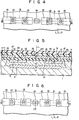
- Fig. 3 is the cross-sectional view as taken along line III-III in Fig. 4.
- a laser beam L is directed onto the area in which silicon nitride film 21 is in contact with metal interconnection layer 15, so as to locally heat metal interconnection layer 15 from 400 to 600°C.
- Metal interconnection layer 15 (aluminum alloy) 15, CVD oxide film 17 and silicon nitride film 21 have expansion coefficients of 2.5 x 10 -5 (/deg), 4.0 x 10 -5 (/deg) and 5.0 x 10 -6 (/deg), respectively.
- the expansion coetticient of silicon nitride film 21 is about one order of magnitude smaller than those of metal interconnection layer 15 and CVD oxide film 17. Silicon nitride film 21 is in direct contact with the predetermined trimming area of metal interconnection layer 15.
- metal interconnection layer 15 When the predetermined trimming area of metal interconnection layer 15 is heated, a stress is produced at metal interconnection layer 15 due to differences in thermal expansion coefficients among metal interconnection layer 15, silicon nitride film 21 and CVD oxide film 17, causing migration of atoms and the consequent diffusion of the atoms in metal interconnection layer 15 into silicon nitride film 21. As a result, metal interconnection layer 15 partially disappears and thus metal interconnection layer 15 is trimmed as at 23. By so doing, it is possible to provide a semiconductor device whose interconnection layer 15 has been broken as shown in Figs. 5 and 6.
- Fig. 5 is a cross-sectional view as taken along line V-V in Fig. 6. In this way, resistors 9 are electrically isolated from each other.
- interconnection layer 15 can be trimmed while a small temperature rise prevails, for example, at metal interconnection layer 15 and insulating films 17 and 21. For this reason there occurs no damage, such as a crack, to CVD oxide film 17 and silicon nitride film 21 is in the neighborhood of the broken portion 23 of the interconnection layer 15. Atter the completion of the semiconductor device there is no possibility that metal interconnection layer 15 will be attacked in the semiconductor device and that the reliability with which the device operates will not be lowered. Furthermore, there occurs no damage to not only tield oxide film 11 but also silicon substrate 1 and epitaxial layer 5. In consequence, the reliability of the semiconductor device will not be lowered by such a trimming step.
- this invention will not be restricted thereto.
- this invention can of course be applied to trimming an interconnection layer connecting two resistors on a semiconductor substrate.
- This invention is not limited to trimming the interconnection layer connecting the resistors in or on the semiconductor substrate.
- This invention is also applied to trimming all kinds of interconnection layers.
- Fig. 7 Similar reference numerals are employed to designate parts or elements corresponding to those shown in Figs. 1 to 6. Further explanation is, therefore, omitted.
- three resistors 9 are formed in a parallel array. One end of each resistor 9 is connected to another portion, not shown, of the semiconductor device through aluminum interconnection layer 25. Another end of each resistor 9 is connected to a still another portion, not shown, of the semiconductor device through interconnection layer 27.
- silicon nitride film 21 is in contact with predetermined trimming areas of interconnection layer 25 through openings 19, respectively.
- Silicon oxide film 17 is in contact with another portion ot interconnection layer 25. Even in the arrangement shown in Fig. 7, when a laser beam is directed onto the predetermined trimming area of interconnection layer 25, atoms in interconnection layer 25 migrate, resulting in a breakage of interconnection layer 25. In the arrangement shown in Fig. 7 a resistive value between interconnection layers 25 and 27 can be adjusted by properly breaking the predetermined trimming areas of interconnection layer 25 in a selective fashion. Resistors 9 are not restricted to three in number.
- the CVD oxide film is formed on metal interconnection layer 15, 25, openings 19 are formed in the portion of CVD oxide film 17 and silicon nitride film 21 is formed on the whole surface of the resultant structure.
- CVD oxide film 17 and silicon nitride film 21 may be formed in reverse order.
- Field oxide film 33 is formed on the surface of P type silicon substrate 31 and an aluminum alloy is evaporated on field oxide film 33, followed by performing a patterning step to provide an interconnection layer.
- a silicon nitride is deposited on the whole surface of the resultant structure to form a silicon nitride film.
- the silicon nitride film is patterned, leaving silicon nitride film 37 on only the specific portion of interconnection layer 35.
- CVD oxide film 39 serving as passivation film, is formed on the whole surface of the resultant structure, thereby obtaining a semiconductor device whose arrangement is shown in Fig. 8.
- a laser beam L is selectively directed onto the portion or portions of the interconnection layer 35, which are in contact with silicon nitride film 37, to cause interconnection layer 35 to be heated locally.
- the atoms in interconnection layer 35 migrate, t'ius breaking interconnection layer 35 as shown in Fig. 9.
- the silicon nitride film has been formed beneath the CVD oxide film, this method can still gain the same advantages as in the first embcdiment.
- the interconnection layer formed of the aluminum alloy has been explained as being completely broken, this invention is not restricted to these embodiments.
- the interconnection layer may be partially dissipated in place of completely breaking the interconnection layer. This can be achieved by properly adjusting the diameter and energy dosage of the laser beam as well as the irradiation time of the laser beam. Only the portion of the interconnection layer can be dissipated by forming the silicon nitride film in contact with only the portion of the interconnection layer. This embodiment will be explained below with reference to Figs. 10 and 11.
- field insulating film 43 is formed to cover a semiconductor substrate 41.
- interconnection layer 45 is formed on field oxide film 43 arid CVD oxide film 47 is formed on the whole surface of the resultant structure.
- arid CVD oxide film 47 is formed on the whole surface of the resultant structure.
- four openings 49 are formed in CVD oxide film to expose only portions of interconnection layer 45 which are situated in a direction of the thickness of interconnection layer 45.
- Silicon nitride film 51 is formed on the whole surface of the resultant structure and interconnection layer 45 directly contacts silicon nitride film 47 only at the locations of regions 49.
- a laser beam is directed onto those portions of the interconnection layer 45 which are in direct contact with silicon nitride film 47.
- atoms migrate in interconnection layer 35, leaving behind dissipated areas 51.
- Fig. 11 atoms migrate in interconnection layer 35, leaving behind dissipated areas 51.
- interconnection layer 45 directly contacts silicon nitride film 47 at four locations of interconnection layer 45 and the atoms migrate at three of the four locations. According to this invention the trimming of the interconnection layer can be partially carried out.
- the resistive value of interconnection layer 45 becomes a target value accurately by trimming interconnection layer 45 by small amounts, while measuring the resistive value of interconnection layer 45 by for example, a tester, and finely adjusting the resistive value of interconnection layer 45.
- a film for migration may be formed beneath aluminum interconnection 15.
- similar reference numerals are employed to designate portions or elements corresponding to those shown in Figs. 1 to 6. Further explanation is, therefore, omitted.
- silicon nitride film or silicon carbide (SiC) 53 is formed in contact with the undersurface of the predetermined trimming area of interconnection layer 15. This invention is not restricted to forming nitride silicon film 53 beneath the predetermined trimming area only.
- silicon nitride film may be formed on the whole surface of the semiconductor device.
- a film for migration can be formed also beneath interconnection layer 15, permitting atoms in the interconnection layer to be accelerated thereinto. It is proved effective that in order to accelerate migration of atoms silicon nitride film 21 is thickly formed on the predetermined trimming area.
- the first insulating film is not restricted to the silicon nitride.
- the first insulating film use may be made of silicon carbide (SiC).
- this invention is not restricted to silicon carbide.
- the feature of this invention resides in that the first insulating film in contact with the predetermined trimming area has a thermal expansion coefficient smaller than that of the second insulating film in contact with an area other than the predetermined trimming area of the interconnection layer.
- the semiconductor substrate may be either of a P conductivity type or of an N conductivity type.
- the semiconductor device is not restricted to a bipolar type. This invention may be applied to either a M OS type or a CMOS type.
- This invention is not restricted to the case where the interconnection layer of the semiconductor device is to be broken (Figs. 5 and 6), and the case where edges of the interconnection layer are partially lacking (Fig. 11).
- "migration" may occur anywhere or at any spot or spots at the interconnection layer.
- this invention is not restricted to trimming the interconnection layer connecting the resistors, etc. This invention may be applied to any interconnection layer or layers where a trimming operation is necessary.
- This invention is not restricted to the use of a laser beam whereby the predetermined trimming area of the interconnection layer or layers is partially heated. According to this invention any kinds of energy beams may be used if the aluminum interconnection layer can be heated locally.
Landscapes
- Internal Circuitry In Semiconductor Integrated Circuit Devices (AREA)
- Design And Manufacture Of Integrated Circuits (AREA)
- Semiconductor Integrated Circuits (AREA)
Applications Claiming Priority (2)
| Application Number | Priority Date | Filing Date | Title |
|---|---|---|---|
| JP59273740A JPS61154146A (ja) | 1984-12-27 | 1984-12-27 | 半導体装置の製造方法 |
| JP273740/84 | 1984-12-27 |
Publications (2)
| Publication Number | Publication Date |
|---|---|
| EP0189598A1 true EP0189598A1 (fr) | 1986-08-06 |
| EP0189598B1 EP0189598B1 (fr) | 1988-10-05 |
Family
ID=17531905
Family Applications (1)
| Application Number | Title | Priority Date | Filing Date |
|---|---|---|---|
| EP85116624A Expired EP0189598B1 (fr) | 1984-12-27 | 1985-12-27 | Procédé de fabrication d'un dispositif semi-conducteur |
Country Status (4)
| Country | Link |
|---|---|
| US (1) | US4692190A (fr) |
| EP (1) | EP0189598B1 (fr) |
| JP (1) | JPS61154146A (fr) |
| DE (1) | DE3565441D1 (fr) |
Cited By (2)
| Publication number | Priority date | Publication date | Assignee | Title |
|---|---|---|---|---|
| DE19619737A1 (de) * | 1995-11-29 | 1997-06-05 | Mitsubishi Electric Corp | Halbleitereinrichtung und Verfahren zum Herstellen einer Halbleitereinrichtung |
| US6004834A (en) * | 1995-11-29 | 1999-12-21 | Mitsubishi Denki Kabushiki Kaisha | Method of manufacturing semiconductor device having a fuse |
Families Citing this family (10)
| Publication number | Priority date | Publication date | Assignee | Title |
|---|---|---|---|---|
| JPH0718964B2 (ja) * | 1987-06-29 | 1995-03-06 | 日本電信電話株式会社 | 集積光デバイスおよびその製造方法 |
| US5025300A (en) * | 1989-06-30 | 1991-06-18 | At&T Bell Laboratories | Integrated circuits having improved fusible links |
| US5675174A (en) * | 1993-01-06 | 1997-10-07 | Rohm Co., Ltd. | Method for using fuse structure in semiconductor device |
| JP2951215B2 (ja) * | 1993-09-10 | 1999-09-20 | レイセオン・カンパニー | 位相マスクレーザによる微細なパターンの電子相互接続構造の製造方法 |
| US5879439A (en) * | 1996-08-01 | 1999-03-09 | Ricoh Company, Ltd. | Recording ink composition and recording method using the same |
| JPH10289950A (ja) * | 1997-04-15 | 1998-10-27 | Oki Electric Ind Co Ltd | 半導体装置の製造方法及び半導体装置 |
| US6040604A (en) * | 1997-07-21 | 2000-03-21 | Motorola, Inc. | Semiconductor component comprising an electrostatic-discharge protection device |
| JP4255142B2 (ja) * | 1998-02-05 | 2009-04-15 | 株式会社ルネサステクノロジ | 半導体装置 |
| US8034724B2 (en) | 2006-07-21 | 2011-10-11 | Semiconductor Energy Laboratory Co., Ltd. | Method for manufacturing semiconductor device |
| US7811911B2 (en) * | 2006-11-07 | 2010-10-12 | Semiconductor Energy Laboratory Co., Ltd. | Method for manufacturing semiconductor device |
Citations (1)
| Publication number | Priority date | Publication date | Assignee | Title |
|---|---|---|---|---|
| EP0090565A2 (fr) * | 1982-03-30 | 1983-10-05 | Fujitsu Limited | Procédé pour couper sélectivement une couche électroconductrice par irradiation avec un faisceau d'énergie |
Family Cites Families (6)
| Publication number | Priority date | Publication date | Assignee | Title |
|---|---|---|---|---|
| US4240094A (en) * | 1978-03-20 | 1980-12-16 | Harris Corporation | Laser-configured logic array |
| US4217570A (en) * | 1978-05-30 | 1980-08-12 | Tektronix, Inc. | Thin-film microcircuits adapted for laser trimming |
| US4179310A (en) * | 1978-07-03 | 1979-12-18 | National Semiconductor Corporation | Laser trim protection process |
| US4585490A (en) * | 1981-12-07 | 1986-04-29 | Massachusetts Institute Of Technology | Method of making a conductive path in multi-layer metal structures by low power laser beam |
| CA1186070A (fr) * | 1983-06-17 | 1985-04-23 | Iain D. Calder | Connexions de polysilicium faites au laser pour systemes a redondance |
| US4606781A (en) * | 1984-10-18 | 1986-08-19 | Motorola, Inc. | Method for resistor trimming by metal migration |
-
1984
- 1984-12-27 JP JP59273740A patent/JPS61154146A/ja active Pending
-
1985
- 1985-12-24 US US06/813,039 patent/US4692190A/en not_active Expired - Lifetime
- 1985-12-27 DE DE8585116624T patent/DE3565441D1/de not_active Expired
- 1985-12-27 EP EP85116624A patent/EP0189598B1/fr not_active Expired
Patent Citations (1)
| Publication number | Priority date | Publication date | Assignee | Title |
|---|---|---|---|---|
| EP0090565A2 (fr) * | 1982-03-30 | 1983-10-05 | Fujitsu Limited | Procédé pour couper sélectivement une couche électroconductrice par irradiation avec un faisceau d'énergie |
Non-Patent Citations (2)
| Title |
|---|
| ELECTRONIC DESIGN, vol. 30, no. 12, 10th June 1982, pages 69-78, Denville, New Jersey, US; D. BURSKY "Top IC performance hinges on gamut of processing gains, from silicon to metal" * |
| IBM TECHNICAL DISCLOSURE BULLETIN, vol. 21, no. 3, August 1978, pages 1124-1125, New York, US; B. AGGARWAL "Laser personalizable resistors" * |
Cited By (4)
| Publication number | Priority date | Publication date | Assignee | Title |
|---|---|---|---|---|
| DE19619737A1 (de) * | 1995-11-29 | 1997-06-05 | Mitsubishi Electric Corp | Halbleitereinrichtung und Verfahren zum Herstellen einer Halbleitereinrichtung |
| US5844295A (en) * | 1995-11-29 | 1998-12-01 | Mitsubishi Denki Kabushiki Kaisha | Semiconductor device having a fuse and an improved moisture resistance |
| US6004834A (en) * | 1995-11-29 | 1999-12-21 | Mitsubishi Denki Kabushiki Kaisha | Method of manufacturing semiconductor device having a fuse |
| DE19619737C2 (de) * | 1995-11-29 | 2003-11-06 | Mitsubishi Electric Corp | Halbleitereinrichtung mit einer Ersatzschaltung und einer Sicherungsschicht und Verfahren zur Herstellung einer derartigen Halbleitereinrichtung |
Also Published As
| Publication number | Publication date |
|---|---|
| JPS61154146A (ja) | 1986-07-12 |
| DE3565441D1 (en) | 1988-11-10 |
| US4692190A (en) | 1987-09-08 |
| EP0189598B1 (fr) | 1988-10-05 |
Similar Documents
| Publication | Publication Date | Title |
|---|---|---|
| US4445268A (en) | Method of manufacturing a semiconductor integrated circuit BI-MOS device | |
| US4256532A (en) | Method for making a silicon mask | |
| US5065221A (en) | Trimming resistor element for microelectronic circuit | |
| EP0041776B2 (fr) | Procédé pour la fabrication d'un dispositif semiconducteur comportant une structure d'isolation | |
| US4017341A (en) | Method of manufacturing semiconductor integrated circuit with prevention of substrate warpage | |
| EP0152615A2 (fr) | Transistor à effet de champ à barrière Schottky et procédé de sa fabrication | |
| EP0166983A2 (fr) | Procédé pour l'exposition sélective des parois latérales d'une rainure et l'application pour la formation d'un contact de substrat en siliciure métallique pour dispositifs isolés par rainures remplies d'un matériau diélectrique | |
| KR100232410B1 (ko) | 표면장착 및 플립칩 기술을 이용한 집적회로 및 그 형성방법 | |
| US4692190A (en) | Trimming of metal interconnection layer by selective migration of metal atoms by energy beams | |
| CA1045724A (fr) | Methode de faconnage de zones de circuit integre delimitees par un isolant dielectrique en creux | |
| US4403392A (en) | Method of manufacturing a semiconductor device | |
| US5284794A (en) | Method of making semiconductor device using a trimmable thin-film resistor | |
| US4692786A (en) | Semi-conductor device with sandwich passivation coating | |
| JPH027471A (ja) | ポリシリコンショットキーダイオード | |
| US4371423A (en) | Method of manufacturing semiconductor device utilizing a lift-off technique | |
| JP2605030B2 (ja) | 直交バイポーラ−トランジスタ | |
| EP0060205A2 (fr) | Verres binaires à bas point de fusion pour aplanir les surfaces de circuits intégrés contenant des rainures d'isolation | |
| EP0056908B1 (fr) | Dispositif semi-conducteur | |
| JPS6364057B2 (fr) | ||
| EP0157446A1 (fr) | Procédé pour la fabrication simultanée de régions semi-conductrices ayant des dopants différents | |
| US6140194A (en) | Method relating to the manufacture of a semiconductor component | |
| US5099308A (en) | Semiconductor device having reverse conductivity-type diffusion layer and semiconductor wiring layer connected by metallic connection wiring layer | |
| US4614666A (en) | Semi-conductor device with sandwich passivation coating | |
| EP0076147A2 (fr) | Procédé pour la fabrication d'un dispositif semiconducteur comportant une région d'isolation | |
| EP0443575B1 (fr) | Procédé de fabrication d'un dispositif semi-conducteur |
Legal Events
| Date | Code | Title | Description |
|---|---|---|---|
| PUAI | Public reference made under article 153(3) epc to a published international application that has entered the european phase |
Free format text: ORIGINAL CODE: 0009012 |
|
| 17P | Request for examination filed |
Effective date: 19851227 |
|
| AK | Designated contracting states |
Kind code of ref document: A1 Designated state(s): DE FR GB |
|
| 17Q | First examination report despatched |
Effective date: 19870721 |
|
| GRAA | (expected) grant |
Free format text: ORIGINAL CODE: 0009210 |
|
| AK | Designated contracting states |
Kind code of ref document: B1 Designated state(s): DE FR GB |
|
| REF | Corresponds to: |
Ref document number: 3565441 Country of ref document: DE Date of ref document: 19881110 |
|
| ET | Fr: translation filed | ||
| PLBE | No opposition filed within time limit |
Free format text: ORIGINAL CODE: 0009261 |
|
| STAA | Information on the status of an ep patent application or granted ep patent |
Free format text: STATUS: NO OPPOSITION FILED WITHIN TIME LIMIT |
|
| 26N | No opposition filed | ||
| PGFP | Annual fee paid to national office [announced via postgrant information from national office to epo] |
Ref country code: FR Payment date: 19971209 Year of fee payment: 13 |
|
| PGFP | Annual fee paid to national office [announced via postgrant information from national office to epo] |
Ref country code: DE Payment date: 19980105 Year of fee payment: 13 |
|
| REG | Reference to a national code |
Ref country code: GB Ref legal event code: 746 Effective date: 19980929 |
|
| PG25 | Lapsed in a contracting state [announced via postgrant information from national office to epo] |
Ref country code: FR Free format text: LAPSE BECAUSE OF NON-PAYMENT OF DUE FEES Effective date: 19990831 |
|
| REG | Reference to a national code |
Ref country code: FR Ref legal event code: ST |
|
| PG25 | Lapsed in a contracting state [announced via postgrant information from national office to epo] |
Ref country code: DE Free format text: LAPSE BECAUSE OF NON-PAYMENT OF DUE FEES Effective date: 19991001 |
|
| REG | Reference to a national code |
Ref country code: GB Ref legal event code: IF02 |
|
| PGFP | Annual fee paid to national office [announced via postgrant information from national office to epo] |
Ref country code: GB Payment date: 20041222 Year of fee payment: 20 |
|
| PG25 | Lapsed in a contracting state [announced via postgrant information from national office to epo] |
Ref country code: GB Free format text: LAPSE BECAUSE OF EXPIRATION OF PROTECTION Effective date: 20051226 |
|
| REG | Reference to a national code |
Ref country code: GB Ref legal event code: PE20 |