EP0189680B1 - Appareil de stabilisation de source d'alimentation - Google Patents
Appareil de stabilisation de source d'alimentation Download PDFInfo
- Publication number
- EP0189680B1 EP0189680B1 EP85309536A EP85309536A EP0189680B1 EP 0189680 B1 EP0189680 B1 EP 0189680B1 EP 85309536 A EP85309536 A EP 85309536A EP 85309536 A EP85309536 A EP 85309536A EP 0189680 B1 EP0189680 B1 EP 0189680B1
- Authority
- EP
- European Patent Office
- Prior art keywords
- output voltage
- power source
- voltage
- source apparatus
- stabilizing power
- Prior art date
- Legal status (The legal status is an assumption and is not a legal conclusion. Google has not performed a legal analysis and makes no representation as to the accuracy of the status listed.)
- Expired - Lifetime
Links
- 230000000087 stabilizing effect Effects 0.000 title claims description 24
- 238000004804 winding Methods 0.000 claims description 36
- 239000003990 capacitor Substances 0.000 claims description 18
- 238000009499 grossing Methods 0.000 claims description 6
- 230000003247 decreasing effect Effects 0.000 description 10
- 238000010586 diagram Methods 0.000 description 5
- 238000004519 manufacturing process Methods 0.000 description 2
- 230000008878 coupling Effects 0.000 description 1
- 238000010168 coupling process Methods 0.000 description 1
- 238000005859 coupling reaction Methods 0.000 description 1
- 238000001514 detection method Methods 0.000 description 1
- 238000000034 method Methods 0.000 description 1
- 230000010355 oscillation Effects 0.000 description 1
- 238000004904 shortening Methods 0.000 description 1
- 230000001131 transforming effect Effects 0.000 description 1
Images

Classifications
-
- H—ELECTRICITY
- H02—GENERATION; CONVERSION OR DISTRIBUTION OF ELECTRIC POWER
- H02M—APPARATUS FOR CONVERSION BETWEEN AC AND AC, BETWEEN AC AND DC, OR BETWEEN DC AND DC, AND FOR USE WITH MAINS OR SIMILAR POWER SUPPLY SYSTEMS; CONVERSION OF DC OR AC INPUT POWER INTO SURGE OUTPUT POWER; CONTROL OR REGULATION THEREOF
- H02M3/00—Conversion of DC power input into DC power output
- H02M3/22—Conversion of DC power input into DC power output with intermediate conversion into AC
- H02M3/24—Conversion of DC power input into DC power output with intermediate conversion into AC by static converters
- H02M3/28—Conversion of DC power input into DC power output with intermediate conversion into AC by static converters using discharge tubes with control electrode or semiconductor devices with control electrode to produce the intermediate AC
- H02M3/325—Conversion of DC power input into DC power output with intermediate conversion into AC by static converters using discharge tubes with control electrode or semiconductor devices with control electrode to produce the intermediate AC using devices of a triode or a transistor type requiring continuous application of a control signal
- H02M3/335—Conversion of DC power input into DC power output with intermediate conversion into AC by static converters using discharge tubes with control electrode or semiconductor devices with control electrode to produce the intermediate AC using devices of a triode or a transistor type requiring continuous application of a control signal using semiconductor devices only
- H02M3/338—Conversion of DC power input into DC power output with intermediate conversion into AC by static converters using discharge tubes with control electrode or semiconductor devices with control electrode to produce the intermediate AC using devices of a triode or a transistor type requiring continuous application of a control signal using semiconductor devices only in a self-oscillating arrangement
- H02M3/3385—Conversion of DC power input into DC power output with intermediate conversion into AC by static converters using discharge tubes with control electrode or semiconductor devices with control electrode to produce the intermediate AC using devices of a triode or a transistor type requiring continuous application of a control signal using semiconductor devices only in a self-oscillating arrangement with automatic control of output voltage or current
- H02M3/3387—Conversion of DC power input into DC power output with intermediate conversion into AC by static converters using discharge tubes with control electrode or semiconductor devices with control electrode to produce the intermediate AC using devices of a triode or a transistor type requiring continuous application of a control signal using semiconductor devices only in a self-oscillating arrangement with automatic control of output voltage or current in a push-pull configuration
- H02M3/3388—Conversion of DC power input into DC power output with intermediate conversion into AC by static converters using discharge tubes with control electrode or semiconductor devices with control electrode to produce the intermediate AC using devices of a triode or a transistor type requiring continuous application of a control signal using semiconductor devices only in a self-oscillating arrangement with automatic control of output voltage or current in a push-pull configuration of the parallel type
-
- H—ELECTRICITY
- H02—GENERATION; CONVERSION OR DISTRIBUTION OF ELECTRIC POWER
- H02M—APPARATUS FOR CONVERSION BETWEEN AC AND AC, BETWEEN AC AND DC, OR BETWEEN DC AND DC, AND FOR USE WITH MAINS OR SIMILAR POWER SUPPLY SYSTEMS; CONVERSION OF DC OR AC INPUT POWER INTO SURGE OUTPUT POWER; CONTROL OR REGULATION THEREOF
- H02M3/00—Conversion of DC power input into DC power output
- H02M3/22—Conversion of DC power input into DC power output with intermediate conversion into AC
- H02M3/24—Conversion of DC power input into DC power output with intermediate conversion into AC by static converters
- H02M3/28—Conversion of DC power input into DC power output with intermediate conversion into AC by static converters using discharge tubes with control electrode or semiconductor devices with control electrode to produce the intermediate AC
- H02M3/325—Conversion of DC power input into DC power output with intermediate conversion into AC by static converters using discharge tubes with control electrode or semiconductor devices with control electrode to produce the intermediate AC using devices of a triode or a transistor type requiring continuous application of a control signal
- H02M3/335—Conversion of DC power input into DC power output with intermediate conversion into AC by static converters using discharge tubes with control electrode or semiconductor devices with control electrode to produce the intermediate AC using devices of a triode or a transistor type requiring continuous application of a control signal using semiconductor devices only
- H02M3/33561—Conversion of DC power input into DC power output with intermediate conversion into AC by static converters using discharge tubes with control electrode or semiconductor devices with control electrode to produce the intermediate AC using devices of a triode or a transistor type requiring continuous application of a control signal using semiconductor devices only having more than one ouput with independent control
Definitions
- the present invention relates to a multiple output type stabilizing power source apparatus for generating stabilized AC and DC voltages.
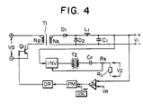
- a typical conventional multiple output type stabilizing power source apparatus as shown in Fig. 4 supplies a stabilized DC voltage to a DC load such as electronic equipment and a stabilized AC voltage to an AC load such as a fluorescent lamp.
- the stabilizing power source apparatus has inverters at the primary and secondary winding sides.
- a reference symbol V0 denotes a DC voltage; Q1, a switching transistor; and T1, an inverter transformer.
- the inverter transformer T1 has a primary winding N P and a secondary winding N S .
- Reference symbols D1 and D2 denote rectifying diodes, respectively; L1, a choke coil; and C1, a smoothing capacitor.
- a reference symbol A1 denotes a differential amplifier for comparing a reference voltage V R with a DC output V1 from the secondary winding N S and generating a signal corresponding to the difference.
- a reference symbol OSC' denotes an oscillator for generating a triangular wave signal; and PM , a pulse width modulator for converting the triangular wave from the oscillator OSC' to pulses of the same frequency as that of the triangular wave and for changing a pulse width of the converted pulses in accordance with a shift of a crossing point between the triangular wave from the oscillator OSC' and the signal from the differential amplifier A1.
- a reference symbol DR denotes a driver for amplifying the pulses from the pulse width modulator PM and for supplying an amplified signal to the base of the transistor Q1.
- a reference symbol INV denotes an inverter for receiving the DC voltage V1 from the secondary winding N S and for generating an AC voltage upon switching; T2, a voltage transformer for transforming the AC voltage from the inverter INV; C F , a waveshaping capacitor; and R L , an AC load for receiving an AC output V2.
- a resistor R S detects a current flowing through the AC load R L , and the inverter INV is switched to keep the current constant in response to the detection signal.
- a rectangular wave current obtained upon switching of the transistor Q1 is rectified by the diodes D1 and D2 connected to the secondary winding N S .
- the rectified current is smoothed by the choke coil L1 and the capacitor C1 to provide the DC output V1.
- the DC output V1 is supplied to the differential amplifier A1 and is compared with the reference input voltage V R .
- the differential amplifier A1 provides a signal corresponding to the difference to the pulse width modulator PM.
- the pulse width modulator PM the triangular wave from the oscillator OSC is converted to the pulses of the same frequency as that of the triangular wave.
- the pulse width is varied in accordance with the crossing point between the leading ramp of the triangular wave and the output from the differential amplifier A1.
- the pulse is amplified by the driver DR, and the amplified pulse is supplied to the base of the transistor Q1.
- the duty factor of the transistor Q1 is thus controlled in response to the output from the differential amplifier A1. Therefore, the DC voltage V1 is kept constant.
- the stabilized DC output V1 is supplied to the inverter INV and is converted to the AC voltage upon its switching.
- the AC voltage is boosted by the transformer T2.
- the boosted voltage is then smoothed by the capacitor C F , and the smoothed output is supplied to the AC load R L .
- This stabilizing power source apparatus has a transformer having a primary winding, a direct current being input to the primary winding via a switching device, the transformer having first and second secondary windings.
- a first rectification/smoothing circuit is connected across the first secondary winding and provides the first DC output voltage and second rectification/smoothing circuit is connected across the second secondary winding and provides the second DC output voltage.
- a first differential amplifier compares a first reference voltage with the first DC output voltage and generates a first differential signal according to a difference between the first DC output voltage and that first reference signal.
- a second differential amplifier compares a second reference voltage with the second DC output voltage and generates a second differential signal according to the difference between the second DC output voltage and the second reference voltage.
- the second differential signal is used to control the frequency of an oscillator, the output of which is supplied to a pulse width modulator.
- the output width of the pulse is the pulse width modulator is controlled by the first differential signal.
- the output of the pulse width modulator is applied, via a driver, to the switching device. It is an object of the present invention to provide a stabilizing power source apparatus with low-level common mode noise.
- a stabilizing power source apparatus having a DC output voltage and an AC output voltage
- a transformer having a primary winding, a direct current being input to said primary winding via a switching device, said transformer having first and second secondary windings, a rectification / smoothing circuit connected across said first secondary winding and providing said DC output voltage, a resonance circuit which connects said second secondary winding to an AC load and outputs said AC output voltage to said AC load, a first differential amplifier for comparing a first reference voltage with said DC output voltage and for generating a first differential signal according to a difference between said DC output voltage and said first reference voltage, a resistor for providing an output voltage representative of the current flowing through said AC load, a second differential amplifier for comparing a second reference voltage with the output voltage of said resistor and for generating a second differential signal according to the difference between said output voltage of said resistor and said second reference voltage, a pulse modulator which is connected to the outputs of the first and second differential amplifiers and which produces a
- Fig. 1 is a circuit diagram of a stabilizing power source apparatus according to an embodiment of the present invention.
- the same reference numerals as in Fig. 4 denote the same parts in Fig. 1.
- a reference symbol V0 denotes an input DC voltage; Q1, a switching element; and T3, an inverter transformer.
- the inverter transformer T3 has a primary winding N P , a DC voltage output secondary winding N S1 magnetically coupled to the primary winding N P , and an AC output secondary winding N S2 magnetically coupled to the primary winding N P .
- the switching element Q1 comprises a bipolar transistor but can be replaced with a GTO thyristor, a normal thyristor or the like.
- Reference symbols D1 and D2 denote rectifying diodes for the secondary winding N S1 ; L1, a choke coil; C1, a smoothing capacitor; L2, a choke coil for the secondary winding N S2 ; C3, a filter capacitor; R S , a resistor for detecting a load current; and R L , an AC load.
- a reference symbol A1 denotes a differential amplifier for comparing a reference input voltage V R1 with the DC voltage from the secondary winding N S1 and generating a signal representing the difference therebetween.
- a reference symbol A2 denotes a differential amplifier for receiving the AC voltage from the load current detecting resistor R S inserted between the secondary winding N S2 and the load R L , comparing the AC voltage with a reference input voltage V R2 and generating a signal representing the difference therebetween.
- a reference symbol OSC' denotes an oscillator for generating a triangular wave, the leading ramp of which is changed in response to the signal from the differential amplifier A2.
- a reference symbol PM denotes a pulse modulator for comparing the output signal from the differential amplifier A1 with the triangular wave from the oscillator OSC' and generating a pulse, the width and frequency of which are changed in accordance with the shift of the crossing point between these input signals.
- a reference symbol DR denotes a driver for amplifying the pulse and supplying an amplified signal to the base of the transistor Q1.
- the duty factor of the transistor Q1 is controlled to keep the DC output voltage V1 constant.
- the switching frequency of the transistor Q1 is controlled to keep the AC load current constant.
- Fig. 2 is a graph showing the relationship between input impedance Z and frequency f when the AC load R L is viewed from the secondary winding N S2 .
- the switching frequency f of the transistor Q1 is decreased. Accordingly, the input impedance Z is increased and the load current is decreased (P1 in Fig. 2).
- the switching frequency f of the transistor Q1 is increased. Accordingly, the input impedance Z is increased, and the load current is also increased (P2 in Fig. 2).
- Fig. 3 is a circuit diagram of the oscillator OSC' in the apparatus in Fig. 1.
- reference symbols R11 to R17 denote resistors; C11 and C12, capacitors; Q11 to Q13, transistors; IC1, an integrated circuit element as a timer circuit; and IC2, an integrated circuit element as a NAND gate.
- the timer circuit IC1 generates a clock signal with a period T at an output terminal OUT thereof so as to charge the capacitor C11 in accordance with a time constant determined by the resistance of the resistor R15 and the capacitance of the capacitor C11, and at the same time, discharge the capacitor C11 in accordance with a time constant determined by the resistance of the resistor R17 and the capacitance of the capacitor C11.
- the clock signal is supplied to the base of the transistor Q13 through the NAND gate IC2, so that the triangular wave voltage appears across the capacitor C12 upon ON/OFF operation of the transistor Q13.
- the triangular wave voltage signal is supplied from the collector of the transistor Q13 to the pulse modulator PM.
- the transistor Q11 When the AC voltage V2 is constant and the signal from the differential amplifier A2 is the reference voltage value, the transistor Q11 is turned off.
- the timer circuit IC1 generates the clock signal of a predetermined frequency.
- the internal resistance of the transistor Q11 is decreased and the charge rate of the capacitor C11 is increased. As a result, the period T of the clock signal is shortened.
- the internal resistance of the transistor Q12 is decreased to increase the charge rate of the capacitor C12.
- the leading ramp of the triangular wave becomes steep.
- the leading ramp of the triangular wave becomes moderate in the reverse process.
- the frequency of the oscillator OSC' varies in accordance with variations in the output signal from the differential amplifier A2 which, in turn, varies in accordance with variations in that AC output load current.
- the width and frequency of the pulse supplied to the base of the switching transistor Q1 vary in accordance with the variations in the voltage from the differential amplifier A1 and the frequency of the triangular wave from the oscillator OSC'.
- the duty factor and the switching frequency of the transistor Q1 are controlled to keep the DC voltage V1 and the AC voltage V2 constant.
- the inverter at the primary winding comprises a forward type inverter.
- the present invention is not limited to this arrangement.
- a half-bridge type inverter or a full-bridge type inverter can be used in place of the forward type inverter.
- the pulse width and frequency control circuit is exemplified by a PUM consisting of a variable frequency triangular wave oscillator and a comparator in the above description.
- the output signals from the two amplifiers can be supplied to an astable multivibrator to control the ON time intervals of transistors constituting the astable multivibrator. Therefore, the switching frequency and the ON time intervals can be simultaneously controlled.
- the stabilizing power source apparatus has a single switching circuit, so that the number of components is decreased and the manufacturing cost is decreased.
- the apparatus is made small as a whole, and its reliability is improved.
Landscapes
- Engineering & Computer Science (AREA)
- Power Engineering (AREA)
- Dc-Dc Converters (AREA)
- Inverter Devices (AREA)
Claims (6)
- Appareil d'alimentation stabilisée présentant une tension de sortie continue et une tension de sortie alternative, comprenant :
un transformateur (T₃) comportant un enroulement primaire (NP), un courant continu étant entré sur ledit enroulement primaire (NP) via un dispositif de commutation (Q₁), ledit transformateur (T₃) comportant des premier et second enroulements secondaires (NS1, NS2) ;
un circuit de redressage/lissage (D₁, D₂, L₁, C₁) connecté aux bornes dudit premier enroulement secondaire (NS1) et produisant ladite tension de sortie continue ;
un circuit de résonance (L₂, C₃) qui connecte ledit second enroulement secondaire (NS2) à une charge alternative et qui émet en sortie ladite tension de sortie alternative pour ladite charge alternative ;
un premier amplificateur différentiel (A₁) pour comparer une première tension de référence à ladite tension de sortie continue et pour générer un premier signal différentiel en fonction d'une différence entre ladite tension de sortie continue et ladite première tension de référence ;
une résistance (RS) pour produire une tension de sortie représentative du courant qui circule au travers de ladite charge alternative ;
un second amplificateur différentiel (A₂) pour comparer une seconde tension de référence à la tension de sortie de ladite résistance et pour générer un second signal différentiel en fonction de la différence entre ladite tension de sortie de ladite résistance et ladite seconde tension de référence ;
un modulateur d' impulsions (PM) qui est connecté aux sorties des premier et second amplificateurs différentiels (A₁, A₂) et qui produit un train d'impulsions dont la largeur d'impulsion et la fréquence varient en fonction dudit premier signal différentiel et dudit second signal différentiel, le coefficient d'utilisation du train d'impulsions étant variable pour maintenir la tension de sortie continue constante et la fréquence du train d'impulsions étant variable pour maintenir le courant de charge alternative constant ; et
un dispositif de commande pour commander ledit élément de commutation (Q₁) en fonction du signal de sortie dudit modulateur d'impulsions (PM). - Appareil d'alimentation stabilisée selon la revendication 1, dans lequel ledit circuit de résonance comporte une bobine (L₂) et une capacité (C₃) en série.
- Appareil d'alimentation stabilisée selon la revendication 1, dans lequel ledit circuit de résonance comporte une bobine (L₂).
- Appareil d'alimentation stabilisée selon la revendication 1, dans lequel ledit circuit de résonance comporte une capacité (C₃).
- Appareil d'alimentation stabilisée selon la revendication 1, dans lequel ladite charge alternative est une lumière fluorescente.
- Appareil d'alimentation stabilisée selon la revendication 1, dans lequel ledit modulateur d'impulsions (PM) comprend un oscillateur qui génère une onde triangulaire dont la fréquence est modifiée en réponse au signal de sortie en provenance dudit second amplificateur différentiel (A₂), qui convertit l'onde triangulaire en un train d'impulsions de la même fréquence que celle de l'onde triangulaire et qui modifie la largeur d'impulsion des impulsions en fonction d'un décalage d'un point de croisement entre une rampe avant de l'onde triangulaire et le signal de sortie en provenance dudit premier amplificateur différentiel (A₁).
Priority Applications (1)
| Application Number | Priority Date | Filing Date | Title |
|---|---|---|---|
| EP91202705A EP0471421B1 (fr) | 1984-12-28 | 1985-12-30 | Appareil de source de puissance stabilisante |
Applications Claiming Priority (4)
| Application Number | Priority Date | Filing Date | Title |
|---|---|---|---|
| JP27771784A JPS61157263A (ja) | 1984-12-28 | 1984-12-28 | 安定化電源装置 |
| JP277717/84 | 1984-12-28 | ||
| JP28092284A JPS61161964A (ja) | 1984-12-29 | 1984-12-29 | 安定化電源装置 |
| JP280922/84 | 1984-12-29 |
Related Child Applications (1)
| Application Number | Title | Priority Date | Filing Date |
|---|---|---|---|
| EP91202705.9 Division-Into | 1991-10-18 |
Publications (3)
| Publication Number | Publication Date |
|---|---|
| EP0189680A2 EP0189680A2 (fr) | 1986-08-06 |
| EP0189680A3 EP0189680A3 (en) | 1988-03-16 |
| EP0189680B1 true EP0189680B1 (fr) | 1993-02-10 |
Family
ID=26552531
Family Applications (2)
| Application Number | Title | Priority Date | Filing Date |
|---|---|---|---|
| EP85309536A Expired - Lifetime EP0189680B1 (fr) | 1984-12-28 | 1985-12-30 | Appareil de stabilisation de source d'alimentation |
| EP91202705A Expired - Lifetime EP0471421B1 (fr) | 1984-12-28 | 1985-12-30 | Appareil de source de puissance stabilisante |
Family Applications After (1)
| Application Number | Title | Priority Date | Filing Date |
|---|---|---|---|
| EP91202705A Expired - Lifetime EP0471421B1 (fr) | 1984-12-28 | 1985-12-30 | Appareil de source de puissance stabilisante |
Country Status (3)
| Country | Link |
|---|---|
| US (1) | US4677534A (fr) |
| EP (2) | EP0189680B1 (fr) |
| DE (2) | DE3588108T2 (fr) |
Families Citing this family (63)
| Publication number | Priority date | Publication date | Assignee | Title |
|---|---|---|---|---|
| JPS62233067A (ja) * | 1986-03-31 | 1987-10-13 | Toshiba Corp | 安定化電源装置 |
| US4772995A (en) * | 1987-01-08 | 1988-09-20 | Veeco Instruments Inc. | Switching supply with pulse width and rate modulation |
| US4855885A (en) * | 1988-04-11 | 1989-08-08 | Dsl Dynamic Sciences Limited | Light beam intensifier |
| US4893227A (en) * | 1988-07-08 | 1990-01-09 | Venus Scientific, Inc. | Push pull resonant flyback switchmode power supply converter |
| DE3828959A1 (de) * | 1988-08-26 | 1990-03-08 | Ant Nachrichtentech | Schaltregler |
| CA1316980C (fr) * | 1988-12-27 | 1993-04-27 | Daniel C. Hughey | Bloc d'alimentation |
| US5128593A (en) * | 1990-01-25 | 1992-07-07 | Beckman Instruments, Inc. | Power supply for gas-filled lamps |
| US5448469A (en) * | 1990-02-15 | 1995-09-05 | Deutsche Thomson-Brandt Gmbh | Switch mode power supply with output feedback isolation |
| US5231563A (en) * | 1990-09-07 | 1993-07-27 | Itt Corporation | Square wave converter having an improved zero voltage switching operation |
| US5126931A (en) * | 1990-09-07 | 1992-06-30 | Itt Corporation | Fixed frequency single ended forward converter switching at zero voltage |
| US5084666A (en) * | 1990-10-23 | 1992-01-28 | International Business Machines Corporation | Switchable output voltage converter |
| US5113337A (en) * | 1991-02-08 | 1992-05-12 | General Electric Company | High power factor power supply |
| US5132889A (en) * | 1991-05-15 | 1992-07-21 | Ibm Corporation | Resonant-transition DC-to-DC converter |
| US5285367A (en) * | 1992-02-07 | 1994-02-08 | Power Integrations, Inc. | Linear load circuit to control switching power supplies under minimum load conditions |
| JP3332407B2 (ja) * | 1992-02-28 | 2002-10-07 | キヤノン株式会社 | 画像形成装置 |
| GB9214896D0 (en) * | 1992-07-14 | 1992-08-26 | Attwood Brian E | A low cost 1mhz ferrite regulated converter |
| US5479087A (en) * | 1992-10-02 | 1995-12-26 | Compaq Computer Corp. | Synchronized switch tapped coupled inductor regulation circuit |
| EP0689731A1 (fr) * | 1993-03-17 | 1996-01-03 | National Semiconductor Corporation | Circuit de glissemant de fréquence pour régulateur à découpage |
| JP2758552B2 (ja) * | 1993-08-27 | 1998-05-28 | 浜松ホトニクス株式会社 | プッシュプル共振型スイッチング電源回路 |
| US5640315A (en) * | 1994-03-18 | 1997-06-17 | Nippon Steel Corporation | Switching regulator |
| DE4424800A1 (de) * | 1994-07-14 | 1996-01-18 | Philips Patentverwaltung | Schaltungsanordnung zum Liefern von Speisespannungen |
| KR0150384B1 (ko) * | 1995-05-31 | 1998-10-15 | 배순훈 | 고압안정화회로 |
| US5690693A (en) * | 1995-06-07 | 1997-11-25 | Sulzer Intermedics Inc. | Transcutaneous energy transmission circuit for implantable medical device |
| US5702431A (en) * | 1995-06-07 | 1997-12-30 | Sulzer Intermedics Inc. | Enhanced transcutaneous recharging system for battery powered implantable medical device |
| US5745358A (en) * | 1996-05-01 | 1998-04-28 | Compaq Computer Corporation | Variable-frequency converter with constant programmed delay |
| US5973939A (en) * | 1996-08-29 | 1999-10-26 | Trw Inc. | Double forward converter with soft-PWM switching |
| US7269034B2 (en) | 1997-01-24 | 2007-09-11 | Synqor, Inc. | High efficiency power converter |
| EP0954899A2 (fr) | 1997-01-24 | 1999-11-10 | Fische, LLC | Convertisseur de puissance a haute efficacite |
| US6130509A (en) * | 1999-01-22 | 2000-10-10 | Dell Computer Corporation | Balanced feedback system for floating cold cathode fluorescent lamps |
| US6461292B1 (en) | 1999-08-12 | 2002-10-08 | Obtech Medical Ag | Anal incontinence treatment with wireless energy supply |
| US6464628B1 (en) | 1999-08-12 | 2002-10-15 | Obtech Medical Ag | Mechanical anal incontinence |
| US6471635B1 (en) | 2000-02-10 | 2002-10-29 | Obtech Medical Ag | Anal incontinence disease treatment with controlled wireless energy supply |
| US6482145B1 (en) | 2000-02-14 | 2002-11-19 | Obtech Medical Ag | Hydraulic anal incontinence treatment |
| CN1222254C (zh) * | 2000-02-10 | 2005-10-12 | 波滕西亚医疗公司 | 用无线能量源进行尿失禁治疗 |
| MXPA02007589A (es) | 2000-02-10 | 2004-08-23 | Potencia Medical Ag | Tratamiento controlado de incontinencia urinaria. |
| DE60110747T2 (de) | 2000-02-10 | 2006-02-23 | Potencia Medical Ag | Mechanische vorrichtung zur impotenzbehandlung |
| WO2001058393A1 (fr) | 2000-02-11 | 2001-08-16 | Potencia Medical Ag | Appareil de traitement de l'impuissance avec unite de transformation d'energie |
| US20030100929A1 (en) | 2000-02-14 | 2003-05-29 | Peter Forsell | Controlled penile prosthesis |
| DE60119081T2 (de) | 2000-02-14 | 2007-01-04 | Potencia Medical Ag | Männliche impotentzprothesevorrichtung mit drahtloser energieversorgung |
| EP1255513B1 (fr) | 2000-02-14 | 2005-05-25 | Potencia Medical AG | Prothese penienne |
| KR100369834B1 (ko) * | 2000-12-27 | 2003-01-30 | 삼성전자 주식회사 | 디스플레이 장치의 전원제어시스템 및 그 제어방법 |
| EP1225680B1 (fr) * | 2001-01-22 | 2009-11-11 | STMicroelectronics S.r.l. | Alimentation de puissance à découpage |
| EP1257048B1 (fr) * | 2001-05-09 | 2017-10-04 | Philips Lighting Holding B.V. | Dispositif de régulation pour convertisseur résonant |
| DE10122534A1 (de) * | 2001-05-09 | 2002-11-21 | Philips Corp Intellectual Pty | Resonanter Konverter |
| JP5264765B2 (ja) * | 2006-12-21 | 2013-08-14 | オスラム ゲーエムベーハー | 光源の電気負荷などに給電するためのセル、その回路構成、及び、その設計方法 |
| CN101399498B (zh) * | 2007-09-26 | 2013-08-28 | 华为技术有限公司 | 直流转换电源装置及改进直流转换电源装置的方法 |
| WO2010042045A1 (fr) | 2008-10-10 | 2010-04-15 | Milux Holding S.A. | Système, appareil et procédé de traitement de patiente à dysfonctionnement sexuel |
| US7764517B2 (en) * | 2007-11-02 | 2010-07-27 | National Semiconductor Corporation | Power supply with reduced power consumption when a load is disconnected from the power supply |
| BRPI0819622B8 (pt) | 2007-11-27 | 2021-06-22 | Implantica Patent Ltd | controle de transferência de energia adaptado para um sistema de dispositivo médico |
| EP2244760B8 (fr) | 2008-01-28 | 2022-07-20 | Implantica Patent Ltd. | Dispositif de drainage implantable |
| EP2240138B1 (fr) | 2008-01-29 | 2021-07-21 | Implantica Patent Ltd. | Appareil de traitement de l'obésité |
| US7983059B2 (en) * | 2008-09-02 | 2011-07-19 | Analog Devices, Inc. | High frequency power converter based on transformers |
| CA2776450C (fr) | 2008-10-10 | 2018-08-21 | Peter Forsell | Procede, systeme et dispositif d'assistance cardiaque |
| PL2349383T3 (pl) | 2008-10-10 | 2022-09-19 | Medicaltree Patent Ltd. | Urządzenie i system wspomagania serca |
| US8600510B2 (en) | 2008-10-10 | 2013-12-03 | Milux Holding Sa | Apparatus, system and operation method for the treatment of female sexual dysfunction |
| US10219898B2 (en) | 2008-10-10 | 2019-03-05 | Peter Forsell | Artificial valve |
| ES2985873T3 (es) * | 2008-10-10 | 2024-11-07 | Implantica Patent Ltd | Medios de fijación para conjunto de control médico implantable |
| US8149600B2 (en) * | 2009-05-22 | 2012-04-03 | Infineon Technologies Ag | System and method for ringing suppression in a switched mode power supply |
| US10952836B2 (en) | 2009-07-17 | 2021-03-23 | Peter Forsell | Vaginal operation method for the treatment of urinary incontinence in women |
| US9949812B2 (en) | 2009-07-17 | 2018-04-24 | Peter Forsell | Vaginal operation method for the treatment of anal incontinence in women |
| US9293997B2 (en) | 2013-03-14 | 2016-03-22 | Analog Devices Global | Isolated error amplifier for isolated power supplies |
| US10199950B1 (en) | 2013-07-02 | 2019-02-05 | Vlt, Inc. | Power distribution architecture with series-connected bus converter |
| JP7596885B2 (ja) | 2021-03-24 | 2024-12-10 | スミダコーポレーション株式会社 | 出力安定化回路及びdcdcコンバータ回路 |
Family Cites Families (9)
| Publication number | Priority date | Publication date | Assignee | Title |
|---|---|---|---|---|
| NL7101662A (fr) * | 1971-02-09 | 1972-08-11 | ||
| BE791943A (fr) * | 1972-02-18 | 1973-03-16 | Telecomunicazioni Soc It | Regulateur de tension et/ou de courant |
| JPS52203B2 (fr) * | 1972-07-20 | 1977-01-06 | ||
| DE3008887C2 (de) * | 1980-03-07 | 1982-06-24 | Siemens AG, 1000 Berlin und 8000 München | Gegentaktumrichter mit einem sättigbaren Übertrager |
| US4322817A (en) * | 1980-12-29 | 1982-03-30 | Gte Automatic Electric Labs Inc. | Switching regulated pulse width modulated push-pull converter |
| US4451876A (en) * | 1981-06-19 | 1984-05-29 | Hitachi Metals, Ltd. | Switching regulator |
| NL8105160A (nl) * | 1981-11-16 | 1983-06-16 | Philips Nv | Schakeling voor het omzetten van een ingangsgelijkspanning in een uitgangsgelijkspanning. |
| DE3209975A1 (de) * | 1982-03-18 | 1983-09-29 | Nixdorf Computer Ag, 4790 Paderborn | Schaltungsanordnung zur steuerung der hoehe einer abzugebenden pulsierenden spannung, insbesondere in einem gleichspannungswandler |
| US4535399A (en) * | 1983-06-03 | 1985-08-13 | National Semiconductor Corporation | Regulated switched power circuit with resonant load |
-
1985
- 1985-12-30 US US06/814,494 patent/US4677534A/en not_active Expired - Fee Related
- 1985-12-30 EP EP85309536A patent/EP0189680B1/fr not_active Expired - Lifetime
- 1985-12-30 DE DE3588108T patent/DE3588108T2/de not_active Expired - Fee Related
- 1985-12-30 DE DE8585309536T patent/DE3587090T2/de not_active Expired - Fee Related
- 1985-12-30 EP EP91202705A patent/EP0471421B1/fr not_active Expired - Lifetime
Also Published As
| Publication number | Publication date |
|---|---|
| EP0471421A2 (fr) | 1992-02-19 |
| DE3587090T2 (de) | 1993-06-03 |
| US4677534A (en) | 1987-06-30 |
| EP0471421B1 (fr) | 1996-05-22 |
| DE3587090D1 (de) | 1993-03-25 |
| EP0471421A3 (en) | 1993-02-03 |
| DE3588108T2 (de) | 1996-11-07 |
| DE3588108D1 (de) | 1996-06-27 |
| EP0189680A2 (fr) | 1986-08-06 |
| EP0189680A3 (en) | 1988-03-16 |
Similar Documents
| Publication | Publication Date | Title |
|---|---|---|
| EP0189680B1 (fr) | Appareil de stabilisation de source d'alimentation | |
| EP0444428B1 (fr) | Alimentation régulée en modulation de largeur d'impulsion comprenant une bobine d'induction avec 3 enroulements | |
| JP3531385B2 (ja) | 電源装置 | |
| CN1031374C (zh) | 交直流变换器 | |
| US6013969A (en) | Piezoelectric transformer inverter | |
| JP3459142B2 (ja) | 駆動パルス出力制限回路 | |
| US5949199A (en) | Gas discharge lamp inverter with a wide input voltage range | |
| US4761727A (en) | Current sensing circuit for use with decoupled half bridge converter | |
| EP0295858B1 (fr) | Alimentation de puissance à courant continu en haute tension | |
| KR960010828B1 (ko) | 고역률 전원공급장치 | |
| JP2793806B2 (ja) | 電力変換制御装置 | |
| US6038141A (en) | Resonance power supply circuit of variable capacity type | |
| EP0785611A2 (fr) | Appareil d'alimentation de puissance électrique | |
| US5861768A (en) | Resolver exciter having a simple power source unit | |
| JP3328310B2 (ja) | 放電灯点灯装置 | |
| JP3252540B2 (ja) | インバータ装置 | |
| JPH0646561A (ja) | 共振型dc−dcコンバータ | |
| KR100301463B1 (ko) | 공진형고주파가열장치의인버터출력제어회로 | |
| JP2867452B2 (ja) | 周波数同調回路 | |
| JP2801068B2 (ja) | ランプ電圧検出装置 | |
| JP3211380B2 (ja) | 電力変換装置 | |
| JP2719746B2 (ja) | X線電源の制御回路 | |
| JPH08149851A (ja) | 圧電トランス駆動装置 | |
| JPH05161352A (ja) | 共振形コンバータ | |
| JPH06113555A (ja) | 放電管点灯回路 |
Legal Events
| Date | Code | Title | Description |
|---|---|---|---|
| PUAI | Public reference made under article 153(3) epc to a published international application that has entered the european phase |
Free format text: ORIGINAL CODE: 0009012 |
|
| 17P | Request for examination filed |
Effective date: 19860109 |
|
| AK | Designated contracting states |
Kind code of ref document: A2 Designated state(s): DE FR GB IT NL |
|
| PUAL | Search report despatched |
Free format text: ORIGINAL CODE: 0009013 |
|
| AK | Designated contracting states |
Kind code of ref document: A3 Designated state(s): DE FR GB IT NL |
|
| 17Q | First examination report despatched |
Effective date: 19900817 |
|
| GRAA | (expected) grant |
Free format text: ORIGINAL CODE: 0009210 |
|
| AK | Designated contracting states |
Kind code of ref document: B1 Designated state(s): DE FR GB IT NL |
|
| XX | Miscellaneous (additional remarks) |
Free format text: TEILANMELDUNG 91202705.9 EINGEREICHT AM 30/12/85. |
|
| ITF | It: translation for a ep patent filed | ||
| XX | Miscellaneous (additional remarks) | ||
| REF | Corresponds to: |
Ref document number: 3587090 Country of ref document: DE Date of ref document: 19930325 |
|
| ET | Fr: translation filed | ||
| PLBE | No opposition filed within time limit |
Free format text: ORIGINAL CODE: 0009261 |
|
| STAA | Information on the status of an ep patent application or granted ep patent |
Free format text: STATUS: NO OPPOSITION FILED WITHIN TIME LIMIT |
|
| 26N | No opposition filed | ||
| PGFP | Annual fee paid to national office [announced via postgrant information from national office to epo] |
Ref country code: FR Payment date: 19961211 Year of fee payment: 12 |
|
| PGFP | Annual fee paid to national office [announced via postgrant information from national office to epo] |
Ref country code: GB Payment date: 19961223 Year of fee payment: 12 |
|
| PGFP | Annual fee paid to national office [announced via postgrant information from national office to epo] |
Ref country code: NL Payment date: 19961231 Year of fee payment: 12 |
|
| PGFP | Annual fee paid to national office [announced via postgrant information from national office to epo] |
Ref country code: DE Payment date: 19970107 Year of fee payment: 12 |
|
| PG25 | Lapsed in a contracting state [announced via postgrant information from national office to epo] |
Ref country code: GB Free format text: LAPSE BECAUSE OF NON-PAYMENT OF DUE FEES Effective date: 19971230 |
|
| PG25 | Lapsed in a contracting state [announced via postgrant information from national office to epo] |
Ref country code: FR Free format text: THE PATENT HAS BEEN ANNULLED BY A DECISION OF A NATIONAL AUTHORITY Effective date: 19971231 |
|
| PG25 | Lapsed in a contracting state [announced via postgrant information from national office to epo] |
Ref country code: NL Free format text: LAPSE BECAUSE OF NON-PAYMENT OF DUE FEES Effective date: 19980701 |
|
| GBPC | Gb: european patent ceased through non-payment of renewal fee |
Effective date: 19971230 |
|
| NLV4 | Nl: lapsed or anulled due to non-payment of the annual fee |
Effective date: 19980701 |
|
| PG25 | Lapsed in a contracting state [announced via postgrant information from national office to epo] |
Ref country code: DE Free format text: LAPSE BECAUSE OF NON-PAYMENT OF DUE FEES Effective date: 19980901 |
|
| REG | Reference to a national code |
Ref country code: FR Ref legal event code: ST |