EP0189825A2 - Dehnungsaufnehmer - Google Patents
Dehnungsaufnehmer Download PDFInfo
- Publication number
- EP0189825A2 EP0189825A2 EP86100741A EP86100741A EP0189825A2 EP 0189825 A2 EP0189825 A2 EP 0189825A2 EP 86100741 A EP86100741 A EP 86100741A EP 86100741 A EP86100741 A EP 86100741A EP 0189825 A2 EP0189825 A2 EP 0189825A2
- Authority
- EP
- European Patent Office
- Prior art keywords
- strain sensor
- sensor according
- strain
- contacts
- amorphous metal
- Prior art date
- Legal status (The legal status is an assumption and is not a legal conclusion. Google has not performed a legal analysis and makes no representation as to the accuracy of the status listed.)
- Granted
Links
Images
Classifications
-
- G—PHYSICS
- G01—MEASURING; TESTING
- G01L—MEASURING FORCE, STRESS, TORQUE, WORK, MECHANICAL POWER, MECHANICAL EFFICIENCY, OR FLUID PRESSURE
- G01L1/00—Measuring force or stress, in general
- G01L1/20—Measuring force or stress, in general by measuring variations in ohmic resistance of solid materials or of electrically-conductive fluids; by making use of electrokinetic cells, i.e. liquid-containing cells wherein an electrical potential is produced or varied upon the application of stress
- G01L1/22—Measuring force or stress, in general by measuring variations in ohmic resistance of solid materials or of electrically-conductive fluids; by making use of electrokinetic cells, i.e. liquid-containing cells wherein an electrical potential is produced or varied upon the application of stress using resistance strain gauges
- G01L1/2287—Measuring force or stress, in general by measuring variations in ohmic resistance of solid materials or of electrically-conductive fluids; by making use of electrokinetic cells, i.e. liquid-containing cells wherein an electrical potential is produced or varied upon the application of stress using resistance strain gauges constructional details of the strain gauges
-
- G—PHYSICS
- G01—MEASURING; TESTING
- G01B—MEASURING LENGTH, THICKNESS OR SIMILAR LINEAR DIMENSIONS; MEASURING ANGLES; MEASURING AREAS; MEASURING IRREGULARITIES OF SURFACES OR CONTOURS
- G01B7/00—Measuring arrangements characterised by the use of electric or magnetic techniques
- G01B7/16—Measuring arrangements characterised by the use of electric or magnetic techniques for measuring the deformation in a solid, e.g. by resistance strain gauge
- G01B7/24—Measuring arrangements characterised by the use of electric or magnetic techniques for measuring the deformation in a solid, e.g. by resistance strain gauge using change in magnetic properties
-
- G—PHYSICS
- G01—MEASURING; TESTING
- G01L—MEASURING FORCE, STRESS, TORQUE, WORK, MECHANICAL POWER, MECHANICAL EFFICIENCY, OR FLUID PRESSURE
- G01L1/00—Measuring force or stress, in general
- G01L1/12—Measuring force or stress, in general by measuring variations in the magnetic properties of materials resulting from the application of stress
- G01L1/125—Measuring force or stress, in general by measuring variations in the magnetic properties of materials resulting from the application of stress by using magnetostrictive means
Definitions
- the invention relates to a strain sensor according to the preamble of claim 1.
- the known strain transducers are manufactured in a conventional manner with wire-shaped or foil-like resistance elements and also in thin-film technology. They are used as sensors for measuring force, displacement, weight, acceleration or pressure.
- the strain transducers currently most frequently used consist of a semiconductor crystal that exhibits a piezo effect (DE-AS 23 49 463).
- the piezo effect can be measured directly, and on the other hand, the change in conductivity caused by the piezo effect can be measured.
- the strain gauge is attached indirectly by gluing or screwing the crystal onto the substrate to be examined.
- the strain transducers manufactured using thin-film processes are an exception, but like all piezo crystals must be oriented according to their structure. Indirect attachment usually causes hysteresis. In addition to the hysteresis of the piezo effect, there is an inaccuracy of the elongation compared to the compression.
- the crystalline structure of the strain sensor does not allow a strong bending of the piezo crystal, since it breaks easily, and thus limits the application.
- Rapid aging has a particularly disadvantageous effect when measuring the piezo effect, since it requires constant re-calibration
- Strain transducers which are constructed from a metal strip and in which the elongation causes a change in resistance by changing the cross section and length of the strain transducer are very stable. However, this change is very small and therefore only allows an insensitive strain measurement.
- the invention has for its object to provide a strain sensor that has a high sensitivity, is versatile and easy to manufacture
- the strain sensor consists of a ferromagnetic, magnetically anisotropic, magnetostrictive material, which additionally shows galvanomagnetic effects
- the strain sensor according to the invention consisting of amorphous metal, improves the conventional strain sensors. Due to its amorphous structure, it is also easy to manufacture and attach to the substrate like the metal strip, but has the high sensitivity of the semiconductor crystal and thus combines the advantages of existing strain gauges without having their disadvantages. In addition, there is a larger stretch range than with conventional strain transducers, which is due to the amorphous property.
- the use of thin-film technology in the production of the strain sensor favors the production of the electrical contacts in the same way and thus makes contacting considerably easier.
- the strain gauge is manufactured as an amorphous metal by vapor deposition or dusting.
- the mixture makes it necessary that both components are applied according to their proportion.
- the layer is applied to a substrate and then the desired shape of the surface is lithographically etched.
- the dimensions of the layer are 3 mm long, 1 mm wide and between 10 and 100 nm thick.
- the process takes four hours.
- the direction of magnetization impressed in this way is the energetically most favorable direction and the magnetization will always fall back into this most favorable direction at room temperature after a deflection. This direction is also called "easy direction"
- the function of the strain sensor lies in the interaction of several physical properties.
- the magnetization causes an anisotropy of the conductivity.
- the magnetostrictive behavior has a change in the direction of magnetization when the strain sensor experiences a stretch and / or compression.
- the magnetization changes its direction up to 90 ° in proportion to the mechanical stress.
- the strain measuring range is determined by the anisotropy field strength H k .
- H k in turn depends on the material used and the magnetic pretreatment. Since the axis of the anisotropy of conductivity rotates with the magnetization, the electrical resistance between two points, the connecting line of which lies in the plane of rotation, also changes in proportion to the mechanical stress. Elongation or compression can thus be measured as a change in the electrical conductivity.
- the planar Hall effect is used to determine the elongation.
- a different arrangement of the strain sensor is chosen so that a driving current flows through the thin layer as in the normal Hall effect.
- a magnetic field is also necessary in order to move the charge carriers from their original direction due to the Lorentz force that occurs.
- the motive current flows in one direction.
- the component of a magnetic field that is perpendicular to the current direction now causes the charge carriers to be deflected in the third direction, which is perpendicular to the other two.
- the Hall voltage is tapped in this third direction.
- the tape-shaped strain gauge must be connected to the substrate via a side surface in the technique used.
- the planar Hall effect is used in the strain transducer according to the invention, which enables the connection of the large strip area to the substrate. Specifically, this means that the driving current flows in the plane of the thin layer and that the magnetization is also in the plane. In the unstretched state, the magnetization and the driving current lie in parallel. There is therefore no magnetic component perpendicular to the driving current and therefore no Hall effect - (neither planar nor normal). If the magnetization rotates, a component is created and Hall voltage thus occurs.
- the planar Hall voltage is measured perpendicular to the direction of the drive current in the plane spanned by the drive current and magnetization.
- the easy direction lies in the plane of the strip surface and perpendicular to the longitudinal axis.
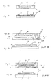
- the two contacts 12 are attached to the ends of the strip 13 so that they each cover the end faces of the strip; in addition, the contacts still adhere to the substrate 11.
- They consist of an alloy of CrAu or CoFeB and are vapor-deposited or sputtered on.
- the change in the electrical conductivity between the two contacts is the measure of the elongation.
- the conductivity is measured electrically.
- This version is particularly suitable for digital display of the stretch. There is a risk that two adjacent domains will short-circuit magnetically, and that parts of the domains will rotate from the easy direction, even without stretching.
- the strain gauge (Fig. 2a, 2b) is built up as a double layer.
- the two FeB strips 23, 24 are separated by an SiO 2 layer 25 such that the strips are in contact with one another at one end 26.
- the contacts 22 are each attached to the other end of the strip, as shown in Fig. 2a. It is necessary to change the stripe shape according to Fig. 2a.
- the layers are successively evaporated or sputtered on. This arrangement causes only one domain to be formed in each strip.
- the easy direction is perpendicular to the longitudinal axis of the strip, the domains of the two strips are antiparallel.
- the elongation is measured via the direct current conductivity as in the exemplary embodiment shown in FIGS. 1 a, 1 b.
- the measurement signal between elongation and compression still shows a hysteresis.
- the magnetization is superimposed on the frequency r with an external alternating electromagnetic field, the H component of which is perpendicular to the easy direction.
- the magnetization thus oscillates with the frequency v around the respective rest position, which is determined by stretching.
- the maximum frequency is in the MH z range.
- the electrical conductivity now oscillates with the frequency v or 2v, or a combination of both frequencies, around a medium conductivity.
- the measured frequency depends on the rest position of the magnetization and the amplitude of the external alternating field.
- the measure of the elongation is the difference between the maximum and minimum amplitude of the conductivity
- FIGS. 3a, 3b The corresponding arrangement is shown in FIGS. 3a, 3b.
- the amorphous layer 33 is applied to the substrate 31 as a strip.
- the easy direction is parallel to the longitudinal axis of the strip.
- the contacts 32 are attached to the ends.
- An insulation layer 34 made of SiO 2 lies above them, the contacts remain free.
- the AC voltage applied here provides the alternating magnetic field.
- the stretch to be recorded does not have to be parallel to the longitudinal axis of the strip, it only has to be transmitted via the stretch strip. Since the signal fluctuates periodically, the DC and AC voltage components can be separated electronically and the relevant signal can be further processed as a pure AC voltage signal.
- FIGS. 4, 5 The following two exemplary embodiments (FIGS. 4, 5) are based on the use of the planar Hall effect.
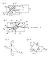
- a circular strain sensor 43 is applied to the substrate 41, five contacts 4 4 to 4 8 being present on the strain sensor.
- the drive current I t flows between the contacts 44 and 45.
- the planar Hall voltage is tapped between the contacts 46 and 47 with 48, the voltage drop along the driving current direction is tapped via the contacts 4 7 and 48 and can thus be taken into account when determining the Hall voltage.
- the easy direction LR. runs parallel to the driving current I t in the unstretched state.
- the strain can be read off directly as a voltage with a constant driving current of 1 t .
- a superposition of the magnetization with an alternating electromagnetic field is also possible when using the planar effect (FIG. 5).
- the sign of the magnetization is also included in the measurement result, ie there is an AC voltage as the Hall voltage.
- the pure alternating voltage signal must first be generated by electronically separating the periodically fluctuating direct voltage signal.
- the Hall voltage oscillates with the frequency of the alternating field v or with 2v or a superposition of both frequencies.
- the measure of the strain is the amplitude of the Hall voltage, which changes in proportion to the strain.
- the strain sensor consists of a Hall probe (Fig. 5);
- the amorphous layer is formed on a substrate 5 1 deposited as a square leaflets 53 at the corners are four electrical contacts mounted 54 to 57.
- the driving current l t is flowing between the contacts 5 4 and 55 and between the contacts 56 and 57 the planar Hall voltage is tapped.
- the direction of stretching s 4 is parallel to the flow direction of the motive current 11 as in FIG. 4.
- the slight direction LR forms an angle of 45 ° with the direction of expansion and lies in the plane of the leaflet.
- the alternating electromagnetic field is generated in a flat coil 52, the turns of which run parallel to the easy direction.
- the AC electrical voltage is applied to contacts 56 and 57 of coil 52.
- strain transducers R h R 2 are attached to a membrane for pressure measurement.
- the strain transducers R and R 4 are not subject to any strain, but are used for temperature compensation when used in a bridge circuit according to FIG. 7.
- U o represents the applied voltage and U s the measurement signal.
- the strain sensor according to the invention does not of course have to consist of an amorphous boron-iron alloy (positive magnetostriction coefficient).
- the amorphous metal of the nickel-iron composition is particularly interesting.
- the magnetostriction coefficient changes its sign for Ni., Fe 19 (atomic percent), which enables further technical designs.
- the amorphous metals show the lowest coercive field strengths, which can be varied by alloying with the metalloids (B, C, Si, Ge, P), zircon or niobium.
- transition metals of the iron group or an alloy consisting of transition metals of the iron group can also be used.
- these show a high coercive field strength and thus a wide hysteresis of the measurement signal.
Landscapes
- Physics & Mathematics (AREA)
- General Physics & Mathematics (AREA)
- Measurement Of Length, Angles, Or The Like Using Electric Or Magnetic Means (AREA)
- Transmission And Conversion Of Sensor Element Output (AREA)
- Control Of High-Frequency Heating Circuits (AREA)
- Fire-Detection Mechanisms (AREA)
- Analysing Materials By The Use Of Radiation (AREA)
Abstract
Description
- Die Erfindung betrifft einen Dehnungsaufnehmer nach dem Oberbegriff des Anspruchs 1.
- Die bekannten Dehnungsaufnehmer werden in herkömmlicher Bauweise mit drahtförmigen oder folienartigen Widerstandselementen sowie auch in Dünnschichttechnik hergestellt. Ihre Anwendung finden sie als Sensoren zur Messung von Kraft, Weg, Gewicht, Beschleunigung oder Druck.
- Die z.Zt am häufigsten benutzten Dehnungsaufnehmer bestehen aus einem Halbleiterkristall, der einen Piezo-Effekt zeight (DE-AS 23 49 463). Hierbei kann zum einen der Piezo-Effekt direkt, zum andem die durch den Piezo-Effekt verursachte Leitfähigkeitsänderung gemessen werden. Die Befestigung des Dehnungsaufnehmers erfolgt dabei in den meisten Fällen indirekt, indem der Kristall auf das zu untersuchende Substrat geklebt oder verschraubt wird. Die Ausnahme bilden die in Dünnschichtverfahren hergestellten Dehnungsaufnehmer, die aber wie alle Piezo-Kristalle nach ihrer Struktur orientiert sein müssen. Die indirekte Befestigung verursacht in der Regel eine Hysterese. Zuzüglich der Hysterese des Piezo-Effekts entsteht eine Meßungenauigkeit der Dehnung gegenüber der Stauchung. Der kristalline Aufbau des Dehnungsaufnehmers läßt keine starke Biegung des Piezo-Kristalls zu, da er leicht bricht, und schränkt somit die Anwendung ein.
- Besonders nachteilig wirkt sich bei der Messung des Piezo-Effekts die schnelle Alterung aus, da sie eine ständige Nacheichung erfordert
- Sehr beständig sind Dehnungsaufnehmer, die aus einem Metallstreifen aufgebaut sind und bei denen die Dehnung dadurch eine Widerstandsänderung hervorruft, daß sich Querschnitt und Länge des Dehnungsaufnehmers ändern. Diese Änderung ist allerdings sehr gering und läßt dadurch nur eine unempfindliche Dehnungsmessung zu.
- Der Erfindung liegt die Aufgabe zugrunde, einen Dehnungsaufnehmer zu schaffen, der eine hohe Empfindlichkeit aufweist, vielseitig verwendbar und einfach herzustellen ist
- Die Aufgabe wird erfindungsgemäß dadurch gelöst, daß der Dehnungsaufnehmer aus einem ferromagnetischen, magnetisch anisotropen, magnetostriktiven Material besteht, das zusätzlich galvanomagnetische Effekte zeigt
- Der erfindungsgemäße Dehnungsaufnehmer, aus amorphem Metall bestehend, verbessert die herkömmlichen Dehnungsaufnehmer. Aufgrund seines amorphen Aufbaus ist er ebenfalls wie der Metallstreifen einfach herzustellen und auf dem Substrat anzubringen, weist aber die hohe Empfindlichkeit des Halbleiterkristalls auf und vereinigt in sich somit die Vorteile bestehender Dehnungsmesser, ohne deren Nachteile zu besitzen. Hierzu kommt noch ein größerer Dehnungsbereich als bei herkömmlichen Dehnungsaufnehmem, der auf die amorphe Eigenschaft zurückzuführen ist. Die Anwendung der Dünnschicht-Technik bei der Herstellung des Dehnungsaufnehmers begünstigt die Herstellung der elektrischen Kontakte auf die gleiche Weise und erleichtert somit die Kontaktierung wesentlich.
- Die Herstellung des Dehnungsaufnehmers als amorphes Metall erfolgt durch Aufdampfen oder Aufstäuben. Die Mischung macht es dabei erforderlich, daß beide Komponenten entsprechend ihrem Anteil aufgebracht werden. Die Schicht wird auf ein Substrat aufgebracht und danach die gewünschte Form der Fläche lithographisch geätzt Die Ausmaße der Schicht liegen bei einer Länge von 3 mm, einer Breite von 1 mm und einer Schichtdicke zwischen 10 bis 100 nm.
- Zur Einprägung der magnetischen Anisotropie wird die Schicht bei T = 300°C getempert, dabei liegt ein Magnetfeld H an, dessen Richtung z.B. parallel zur Fläche verläuft und eine Feldstärke von H2 60 Oe aufweist Der Vorgang dauert vier Stunden. Die derart eingeprägte Richtung der Magnetisierung ist die energetisch günstigste Richtung und die Magnetisierung wird bei Zimmertemperatur nach einer Auslenkung immer wieder in diese günstigste Richtung zurückfallen. Diese Richtung wird auch "leichte Richtung" genannt
- Der Dehnungsaufnehmer ist umso empfindlicher, je kleiner die magnetische Anisotropie der Schicht ist Die Anisotropie wird verkleinert, indem nochmals vier Stunden bei T = 300°C mit Hk 60 Oe getempert wird, wobei das Magnetfeld in der Ebene der Schicht rotiert.
- Die Funktion des Dehnungsaufnehmers liegt im Zusammenwirken mehrerer physikalischer Eigenschaften. Die Magnetisierung bewirkt eine Anisotropie der Leitfähigkeit Das magnetostriktive Verhalten hat eine Änderung der Magnetisierungsrichtung zufolge, wenn der Dehnungsaufnehmer eine Dehnung und/oder Kompression erfährt. Proportional zur mechanischen Beanspruchung ändert die Magnetisierung ihre Richtung bis zu 90°. Der Dehnungsmeßbereich ist dabei durch die Anisotropiefeldstärke Hk bestimmt Hkhängt wiederum vom verwendeten Material und der magnetischen Vorbehandlung ab. Da sich die Achse der Anisotropie der Leitfähigkeit mit der Magnetisierung dreht, verändert sich der elektrische Widerstand zwischen zwei Punkten, deren Verbindungsgerade in der Drehebene liegt, ebenfalls proportional zur mechanischen Beanspruchung. Eine Dehnung oder Stauchung kann somit als Änderung der elektrischen Leitfähigkeit gemessen werden.
- Als zweiter galvanomagnetischer Effekt, neben der Magnetoresistenz, wird der planare Hall-Effekt zur Bestimmung der Dehnung herangezogen. Hierfür wird eine andere Anordnung des Dehnungsaufnehmers so gewählt daß durch die dünne Schicht wie beim normalen Hall-Effekt ein Treibstrom fließt Genauso ist ein Magnetfeld notwendig, um die Ladungsträger aufgrund der auftretenden Lorentzkraft von ihrer ursprünglichen Richtung abzubringen. Der Treibstrom fließt in einer Richtung. Die Komponente eines Magnetfeldes, die senkrecht zur Stromrichtung steht bewirkt nun die Ablenkung der Ladungsträger in die dritte Richtung, die senkrecht zu den beiden anderen steht.
- In dieser dritten Richtung wird die Hall-Spannung abgegriffen. Dabei muß aber bei der verwendeten Technik der bandförmige Dehnungsmeßstreifen über eine Seitenfläche mit dem Substrat verbunden sein. Beim erfindungsgemäßen Dehnungsaufnehmer wird der planare Hall-Effekt ausgenützt, was die Verbindung der großen Streifenfläche mit dem Substrat ermöglicht. Konkret bedeutet dies, daß der Treibstrom in der Ebene der dünnen Schicht fließt und daß die Magnetisierung ebenfalls in der Ebene liegt. Im nicht gedehnten Zustand liegen Magnetisierung und Treibstrom parallel. Es gibt somit keine magnetische Komponente senkrecht zum Treibstrom und somit auch keinen Hall-Effekt - (weder planar noch normal). Dreht sich die Magnetisierung, entsteht eine Komponente und es tritt somit Hall-Spannung auf. Die planare Hall-Spannung wird senkrecht zur Treibstromrichtung in der Ebene, die von Triebstrom und Magnetisierung aufgespannt wird, gemessen.
- Die Erfindung wird im folgenden anhand von durch Figuren veranschaulichten Ausführungsbeispielen näher erläutert.
- Es zeigen
- Fig. 1 eine Anordnung eines einfachen Dehnungsaufnehmers in der Draufsicht,
- Fig. 1b die gemäß Fig. 1a dargestellte Anordnung in einer Seitenansicht,
- Fig. 2a einen doppelbeschichteten Dehnungsaufnehmer in der Draufsicht,
- Fig. 2b die gemäß Fig. 2a dargestellte Anordnung in einer Schnittzeichnung,
- Fig. 3a einen durch ein mangetisches Wechselfeld modulierten Dehnungsaufnehmer,
- Fig. 3b die gemäß Fig. 3a dargestellte Anordnung in einer Schnittzeichnung,
- Fig. 4 die Anordnung eines Dehnungsaufnehmers, bei dem die planare Hall-Spannung abgegriffen wird,
- Fig. 5 die Anordnung eines Dehnungsaufnehmers, bei dem die planare Hall-Spannung abgegriffen und mit einem magnetischen Wechselfeld moduliert wird,
- Fig. 6 einen Dehnungsaufnehmer in der Anwendung eines Druckmessers und
- Fig. 7 eine Brückenschaltung zur Temperaturkompensation.
- In Fig. 1 ist eine amorphe Metallschicht 13, die aus FE80B20 besteht, als Dehnungsmeßstreifen auf ein Substrat 11 aufgebracht Die leichte Richtung liegt in der Ebene der Streifenfläche und senkrecht zur Längsachse. Die beiden Kontakte 12 sind so an den Enden des Streifens 13 angebracht, daß sie jeweils die Stirnseiten des Streifens bedecken; zusätzlich haften die Kontakte noch auf dem Substrat 11. Sie bestehen aus einer Legierung von CrAu oder CoFeB und sind aufgedampft oder aufgestäubt Die Änderung der elektrischen Leitfähigkeit zwischen den beiden Kontakten ist das Maß für die Dehnung. Die Leitfähigkeit wird electrisch gemessen. Diese Ausführung eignet sich besonders zur digitalen Anzeige der Dehnung. Es besteht hierbei die Gefahr, daß sich zwei benachbarte Domänen magnetisch kurzschließen, und daß sich dabei Teile der Domänen, auch ohne Dehnung, aus der leichten Richtung drehen.
- Um die Domänenausbildung vollständig unter Kontrolle zu bringen, wird der Dehnungsmesser (Fig. 2a, 2b) als Doppelschicht aufgebaut. Die beiden FeB-Streifen 23, 24 sind so durch eine SiO,-Schicht 25 getrennt, daß sich die Streifen an einem Ende 26 miteinander Kontakt haben. Die Kontakte 22 sind jeweils am anderen Ende des Streifens, wie in Fig. 2a dargestellt angebracht. Es ist dabei notwendig, die Streifenform nach Abb. 2a zu verändern. Die Schichten werden nacheinander aufgedampft oder aufgestäubt Diese Anordnung bewirkt, daß in jedem Streifen nur eine Domäne gebildet wird. Die leichte Richtung liegt dabei jeweils senkrecht zur Längsachse des Streifens, die Domänen der beiden Streifen liegen antiparallel. Die Dehnung wird wie im in Fig 1 a, 1 b dargestellten Ausführungsbeispiel über die Gleichstromleitfähigkeit gemessen.
- Bei den obengenannten Ausführungsbeispielen zeigt das Meßsignal zwischen Dehnung und Kompression noch eine Hysterese. Um diese zu unterdrücken, wird die Magnetisierung mit einem extemen elektromagnetischen Wechselfeld der Frequenzr überlagert, dessen H-Komponente senkrecht zur leichten Richtung steht Die Magnetisierung oszilliert somit mit der Frequenzv um die jeweilige Ruhelage, die durch Dehnung bestimmt wird. Die maximale Frequenz liegt im MHz-Bereich. Die elektrische Leitfähigkeit oszilliert nun, mit der Frequenzv oder 2v, oder einer Kombination beider Frequenzen, um eine mittlere Leitfähigkeit. Die gemessene Frequenz hängt von der Ruhelage der Magnetisierung und der Amplitude des externen Wechselfeldes ab. Das Maß für die Dehnung ist die Differenz zwischen maximaler und minimaler Amplitude der Leitfähigkeit
- Die entsprechende Anordnung ist in Fig. 3a, 3b dargestellt Auf das Substrat 31 ist die amorphe Schicht 33 als Streifen aufgebracht. Die leichte Richtung liegt parallel zur Längsachse des Streifens. An den Enden sind die Kontakte 32 angebracht Darüber liegt eine Isolationsschicht 34 aus SiO2, die Kontakte bleiben frei. Über der Isolationsschicht 34 befindet sich eine streifenförmige Schicht 35 aus CrAu oder Al, deren Richtung parallel zum FeB-Streifen 33 verläuft Die hier angelegte Wechselspannung sorgt für das magnetische Wechselfeld.
- Die zu erfassende Dehnung muß nicht parallel zur Längsachse des Streifens erfolgen, sie muß nur über den Dehnungsstreifen übertragen werden. Da das Signal periodisch schwankt, kann Gleich- und Wechselspannungsanteil elektronisch getrennt und das relevante Signal als reines Wechelspannungssignal weiterverarbeitet werden.
- Den folgenden beiden Ausführungsbeispielen (Fig. 4, 5) liegt die Anwendung des planaren Hall-Effekts zugrunde. In Fig. 4 ist ein kreisförmiger Dehnungsaufnehmer 43 auf das Substrat 41 aufgebracht wobei am Dehnungsaufnehmer fünf Kontakte 44 bis 48 anliegen. Zwischen den Kontakten 44 und 45 fließt der Treibstrom It. Zwischen den Kontakten 46 und 47 mit 48 wird die planare Hall--Spannung abgegriffen, dabei wird über die Kontakte 47 und 48 der Spannunggsabfall entlang derTreibstromrichtung abgegriffen und kann somit bei der Bestimmung der Hall-Spannung berücksichtigt werden. Die leichte Richtung LR. verläuft im ungedehnten Zustand parallel zum Treibstrom It. Günstigerweise bilden die mechanische Spannung und die Flußrichtung lt im ungedehnten Zustand einen Winkel von p =45°. Mit UH- sin 2p bedeutet dies auf jeden Fall eine Spannungsabnahme bei Dehnung, ausgehend von einer maximalen Hall-Spannung.
- Die Dehnung läßt sich bei konstantem Treibstrom 1 tdirekt als Spannung ablesen.
- Eine Überlagerung der Magnetisierung mit einem elektromagnetischen Wechselfeld, wie sie bei der Anwendung der Magnetoresistenz in den Ausführungsbeispielen in Fig. 2 zu Fig. 3 vorgesehen ist ist bei der Anwendung des planaren Effekts ebenfalls mögjich (Fig. 5). Dabei geht zusätzlich noch das Vorzeichen der Magnetisierung in das Meßergebnis ein, d.h. es liegt eine Wechselspannung als Hall-Spannung an. (Bei der Magnetoresistenz muß das reine Wechselspannungssignal erst durch elektronische Trennung des periodisch schwankenden Gleichspannungssignales erzeugt werden.) Die Hall-Spannung oszilliert wie beim Ausführungsbeispiel von Fig. 3a, 3b mit der Frequenz des Wechselfeldes v oder mit 2v oder einer Überlagerung beider Frequenzen. Das Maß für die Dehnung ist die Amplitude der Hall-Spannung, die sich proportional zur Dehnung ändert Der Dehnungsaufnehmer besteht aus einer Hall--Sonde (Fig. 5); dabei ist die amorphe Schicht als quadratisches Blättchen 53 auf ein Substrat 51 aufgedampft An den Ecken sind vier elektrische Kontakte 54 bis 57 angebracht. Der Treibstrom lt fleißt zwischen den Kontakten 54 und 55 und zwischen den Kontakten 56 und 57 wird die planare Hall-Spannung abgegriffen. Die Dehnungsrichtung s liegt wie in Fig. 4 parallel zur Flußrichtung des Treibstromes 11. Die leichte Richtung L.R. bildet mit der Dehnungsrichtung einen Winkel von 45° und liegt in der Ebene des Blättchens. Das elektromagnetische Wechselfeld wird in einer flachen Spule 52 erzeugt, deren Windungen parallel zur leichten Richtung verlaufen. Die elektrische Wechselspannung wird an den Kontakten 56 und 57 der Spule 52 angelegt.
- In Fig. 6 sind zwei erfindungsgemäße Dehnungsaufnehmer Rh R2 auf einer Membran zur Druckmessung angebracht Die Dehnungsaufnehmer R, und R4 unterliegen keiner Dehnung, sondem sie dienen bei Verwendung in einer Brükkenschaltung gemäß Fig. 7 der Temperaturkompensation. Dabei stellt Uo die angelegte Spannung, und Usdas Meßsignal dar.
- Der erfindungsgemäße Dehnungsaufnehmer muß natürlich nicht aus einer amorphen Bor-Eisen-Legierung (positiver Magnetostriktionkoeffizient) bestehen. Besonders interessant ist das amorphe Metall der Zusammensetzung Nickel-Eisen. Der Magnetostriktions-Koeffizient ändert bei Ni., Fe19 (Atomprozent) sein Vorzeichen, was weitere technische Ausführungen ermöglicht. Die amorphen Metalle zeigen die niedrigsten Koerzitivfeldstärken, die sich durch Legierungen mit den Metalloiden (B, C, Si, Ge, P), Zirkon oder Niob variieren lassen.
- Trotzdem können auch ubergangsmetalle der Eisengruppe oder einer Legierung, bestehend aus ubergangsmetallen der Eisengruppe verwendet werden. Diese zeigen aber gegenüber den amorphen Metallen eine hohe Koerzitivfeldstärke und somit eine breite Hysterese des Meßsignals.
Claims (15)
Priority Applications (1)
| Application Number | Priority Date | Filing Date | Title |
|---|---|---|---|
| AT86100741T ATE74205T1 (de) | 1985-01-23 | 1986-01-21 | Dehnungsaufnehmer. |
Applications Claiming Priority (2)
| Application Number | Priority Date | Filing Date | Title |
|---|---|---|---|
| DE3502008 | 1985-01-23 | ||
| DE19853502008 DE3502008A1 (de) | 1985-01-23 | 1985-01-23 | Dehnungsaufnehmer |
Publications (3)
| Publication Number | Publication Date |
|---|---|
| EP0189825A2 true EP0189825A2 (de) | 1986-08-06 |
| EP0189825A3 EP0189825A3 (en) | 1989-07-26 |
| EP0189825B1 EP0189825B1 (de) | 1992-03-25 |
Family
ID=6260453
Family Applications (1)
| Application Number | Title | Priority Date | Filing Date |
|---|---|---|---|
| EP19860100741 Expired - Lifetime EP0189825B1 (de) | 1985-01-23 | 1986-01-21 | Dehnungsaufnehmer |
Country Status (7)
| Country | Link |
|---|---|
| US (2) | US4782705A (de) |
| EP (1) | EP0189825B1 (de) |
| JP (1) | JPS61181902A (de) |
| AT (1) | ATE74205T1 (de) |
| CA (1) | CA1255922A (de) |
| DE (2) | DE3502008A1 (de) |
| ES (1) | ES8802344A1 (de) |
Cited By (5)
| Publication number | Priority date | Publication date | Assignee | Title |
|---|---|---|---|---|
| EP0329479A3 (en) * | 1988-02-19 | 1990-07-04 | Kabushiki Kaisha Toshiba | Strain gage |
| EP0321791A3 (de) * | 1987-12-22 | 1991-10-09 | AlliedSignal Inc. | Magnetischer Dehnungsmessstreifen |
| EP0523025A1 (de) * | 1991-07-08 | 1993-01-13 | Scan-Mag Sense AS | Verfahren zum Messen eines Drehmomentes und/oder axialer Spannungen |
| EP0690296A3 (de) * | 1994-06-27 | 1998-04-29 | Matsushita Electric Industrial Co., Ltd. | Magnetostriktiver Wandler |
| CN107063596A (zh) * | 2011-09-22 | 2017-08-18 | 住友重机械工业株式会社 | 应变传感器的安装结构以及应变测定装置 |
Families Citing this family (45)
| Publication number | Priority date | Publication date | Assignee | Title |
|---|---|---|---|---|
| US4979395A (en) * | 1987-12-22 | 1990-12-25 | Allied-Signal Inc. | Apparatus and method of forming a magnetic domain strain gage |
| US5136883A (en) * | 1990-08-24 | 1992-08-11 | Jannotta Louis J | Liquid level gage system |
| US5654900A (en) * | 1991-01-10 | 1997-08-05 | Ratner; Leah | Method of and apparatus for optimization of structures |
| DE4203124A1 (de) * | 1992-02-04 | 1992-08-13 | Siemens Ag | Taktiler sensor |
| US5681998A (en) * | 1992-06-09 | 1997-10-28 | Yazaki Corporation | Load measuring device for a vehicle |
| US5631559A (en) * | 1993-03-05 | 1997-05-20 | Northeastern University | Method and apparatus for performing magnetic field measurements using magneto-optic kerr effect sensors |
| US5493220A (en) * | 1993-03-05 | 1996-02-20 | Northeastern University | Magneto-optic Kerr effect stress sensing system |
| DE4408762C2 (de) * | 1993-03-16 | 1999-02-11 | Yazaki Corp | Fahrzeuglastmeßvorrichtung |
| FR2714478B1 (fr) * | 1993-12-23 | 1996-01-26 | Thomson Csf | Détecteur de champ magnétique en couches minces. |
| US5505093A (en) * | 1994-11-21 | 1996-04-09 | Brewer Science, Inc. | Homogeneously conductive polymer films as strain gauges |
| US5856617A (en) * | 1997-09-02 | 1999-01-05 | International Business Machines Corporation | Atomic force microscope system with cantilever having unbiased spin valve magnetoresistive strain gauge |
| US6134971A (en) * | 1998-08-27 | 2000-10-24 | University Of Hawaii | Stress induced voltage fluctuation for measuring stress and strain in materials |
| US6579612B1 (en) | 1999-06-24 | 2003-06-17 | International Business Machines Corporation | Magnetostrictive sensor structure |
| US6694822B1 (en) * | 1999-07-20 | 2004-02-24 | Fidelica Microsystems, Inc. | Use of multi-layer thin films as stress sensor |
| US6889555B1 (en) * | 1999-07-20 | 2005-05-10 | Fidelica Microsystems, Inc. | Magnetoresistive semiconductor pressure sensors and fingerprint identification/verification sensors using same |
| DE10023838C2 (de) * | 2000-05-16 | 2002-11-28 | Siemens Ag | Vorrichtung zum Messen einer Wegänderung zwischen Abschnitten eines Bauteils und Verwendung dieser Vorrichtung |
| DE10063535C2 (de) * | 2000-12-20 | 2003-08-14 | Deutsch Zentr Luft & Raumfahrt | Verfahren zur Bestimmung von veränderlichen Zustandsgrößen eines elastischen Systems |
| GB0107182D0 (en) * | 2001-03-22 | 2001-05-09 | Secr Defence | Stress sensor |
| CN1228568C (zh) * | 2001-03-23 | 2005-11-23 | 多孔燃烧器技术销售有限责任公司 | 用于设定空气比率的方法和装置 |
| US6794862B2 (en) * | 2001-05-08 | 2004-09-21 | Ramot At Tel-Aviv University Ltd. | Magnetic thin film sensor based on the extraordinary hall effect |
| US20040164840A1 (en) * | 2003-02-21 | 2004-08-26 | Brown University Research Foundation | Extraordinary hall effect sensors and arrays |
| DE102004032484B3 (de) | 2004-07-05 | 2005-11-24 | Infineon Technologies Ag | Sensor und Verfahren zum Herstellen eines Sensors |
| DE102004032482B4 (de) * | 2004-07-05 | 2008-01-31 | Infineon Technologies Ag | Sensor und Verfahren zum Erfassen einer Verformung |
| DE102004034277B4 (de) * | 2004-07-15 | 2009-12-03 | Infineon Technologies Ag | Vorrichtung, insbesondere in einer integrierten Schaltungsanordnung, und Verfahren zur Erfassung eines mechanischen Stresszustands in einem Halbleitersubstrat |
| DE102005005354A1 (de) * | 2005-02-05 | 2006-08-10 | Bosch Rexroth Aktiengesellschaft | Kraftmessvorrichtung und Dehnungsmesselement |
| US8307715B2 (en) * | 2009-03-24 | 2012-11-13 | Direct Measurments, Inc. | Directly applied read and transmit—digital strain encoder and digital load cell |
| US9394853B2 (en) | 2011-10-12 | 2016-07-19 | Orbital Atk, Inc. | Strain measurement device, a solid rocket motor including same, and related methods |
| US10697760B2 (en) | 2015-04-15 | 2020-06-30 | General Electric Company | Data acquisition devices, systems and method for analyzing strain sensors and monitoring component strain |
| US9909860B2 (en) | 2015-04-15 | 2018-03-06 | General Electric Company | Systems and methods for monitoring component deformation |
| US9557164B2 (en) | 2015-04-15 | 2017-01-31 | General Electric Company | Data acquisition devices, systems and method for analyzing strain sensors and monitoring turbine component strain |
| US9932853B2 (en) | 2015-04-28 | 2018-04-03 | General Electric Company | Assemblies and methods for monitoring turbine component strain |
| US9933321B2 (en) * | 2015-05-14 | 2018-04-03 | Vishay Measurements Group, Inc. | High gage factor strain gage |
| US9846933B2 (en) | 2015-11-16 | 2017-12-19 | General Electric Company | Systems and methods for monitoring components |
| US9953408B2 (en) | 2015-11-16 | 2018-04-24 | General Electric Company | Methods for monitoring components |
| US10012552B2 (en) * | 2015-11-23 | 2018-07-03 | General Electric Company | Systems and methods for monitoring component strain |
| US9967523B2 (en) | 2015-12-16 | 2018-05-08 | General Electric Company | Locating systems and methods for components |
| US9879981B1 (en) | 2016-12-02 | 2018-01-30 | General Electric Company | Systems and methods for evaluating component strain |
| US10132615B2 (en) | 2016-12-20 | 2018-11-20 | General Electric Company | Data acquisition devices, systems and method for analyzing passive strain indicators and monitoring turbine component strain |
| US10126119B2 (en) | 2017-01-17 | 2018-11-13 | General Electric Company | Methods of forming a passive strain indicator on a preexisting component |
| US10872176B2 (en) | 2017-01-23 | 2020-12-22 | General Electric Company | Methods of making and monitoring a component with an integral strain indicator |
| US11313673B2 (en) | 2017-01-24 | 2022-04-26 | General Electric Company | Methods of making a component with an integral strain indicator |
| US10345179B2 (en) | 2017-02-14 | 2019-07-09 | General Electric Company | Passive strain indicator |
| US10502551B2 (en) | 2017-03-06 | 2019-12-10 | General Electric Company | Methods for monitoring components using micro and macro three-dimensional analysis |
| US10451499B2 (en) | 2017-04-06 | 2019-10-22 | General Electric Company | Methods for applying passive strain indicators to components |
| CN108955969B (zh) * | 2018-08-31 | 2021-03-02 | 纳恩博(北京)科技有限公司 | 电阻应变片、感应组件、力传感器和滑板 |
Family Cites Families (20)
| Publication number | Priority date | Publication date | Assignee | Title |
|---|---|---|---|---|
| JPS4218911B1 (de) * | 1965-04-12 | 1967-07-26 | ||
| US3807223A (en) * | 1972-04-20 | 1974-04-30 | Lignes Telegraph Telephon | Stress sensor with digital output |
| US3943481A (en) * | 1972-06-10 | 1976-03-09 | Denki Onkyo Co., Ltd. | Galvano-magnetic effect device |
| US3774134A (en) * | 1972-12-01 | 1973-11-20 | Honeywell Inc | Antisotropic thin film plated wire magnetostrictive transducer |
| US3858138A (en) * | 1973-03-05 | 1974-12-31 | Rca Corp | Tuneable thin film inductor |
| US3838595A (en) * | 1973-03-16 | 1974-10-01 | Lignes Telegraph Telephon | Data acquisition circuit for a magnetostrictive digital thin film sensor |
| SE376077B (de) * | 1973-09-13 | 1975-05-05 | Asea Ab | |
| US4138783A (en) * | 1973-10-09 | 1979-02-13 | Soletanche | Method for measuring stresses or forces |
| JPS5442166A (en) * | 1977-09-10 | 1979-04-03 | Toshiba Corp | Pressure transmitter |
| JPS54113379A (en) * | 1978-02-23 | 1979-09-04 | Nec Corp | Pressure gauge |
| EP0033749B2 (de) * | 1980-02-06 | 1987-11-11 | Hans W. Dipl.-Phys. Keller | Piezoresistive zylinderdosenartige Druckmesszelle |
| JPS56154637A (en) * | 1980-04-30 | 1981-11-30 | Toshiba Corp | Temperature compensating circuit for pressure converter |
| JPS5737233A (en) * | 1980-08-18 | 1982-03-01 | Matsushita Electric Ind Co Ltd | Tension sensor |
| US4374665A (en) * | 1981-10-23 | 1983-02-22 | The United States Of America As Represented By The Secretary Of The Navy | Magnetostrictive devices |
| JPS5884477A (ja) * | 1981-11-13 | 1983-05-20 | Victor Co Of Japan Ltd | プレ−ナ・ホ−ル素子 |
| CA1214660A (en) * | 1982-09-30 | 1986-12-02 | Koichiro Inomata | Torque sensor and method for manufacturing the same |
| US4763030A (en) * | 1982-11-01 | 1988-08-09 | The United States Of America As Represented By The Secretary Of The Navy | Magnetomechanical energy conversion |
| JPS59181575A (ja) * | 1983-03-31 | 1984-10-16 | Toshiba Corp | トルクセンサ |
| US4561314A (en) * | 1983-10-27 | 1985-12-31 | General Electric Company | Magnetoelastic force/pressure sensor |
| DE3346643A1 (de) * | 1983-12-23 | 1985-07-04 | Standard Elektrik Lorenz Ag, 7000 Stuttgart | Sensor fuer magnetisierbare materialien |
-
1985
- 1985-01-23 DE DE19853502008 patent/DE3502008A1/de not_active Withdrawn
-
1986
- 1986-01-16 CA CA000499724A patent/CA1255922A/en not_active Expired
- 1986-01-21 AT AT86100741T patent/ATE74205T1/de not_active IP Right Cessation
- 1986-01-21 DE DE8686100741T patent/DE3684488D1/de not_active Expired - Lifetime
- 1986-01-21 EP EP19860100741 patent/EP0189825B1/de not_active Expired - Lifetime
- 1986-01-22 JP JP61010324A patent/JPS61181902A/ja active Pending
- 1986-01-23 ES ES551152A patent/ES8802344A1/es not_active Expired
-
1987
- 1987-07-10 US US07/073,355 patent/US4782705A/en not_active Expired - Fee Related
-
1988
- 1988-07-22 US US07/222,799 patent/US4884453A/en not_active Expired - Fee Related
Cited By (5)
| Publication number | Priority date | Publication date | Assignee | Title |
|---|---|---|---|---|
| EP0321791A3 (de) * | 1987-12-22 | 1991-10-09 | AlliedSignal Inc. | Magnetischer Dehnungsmessstreifen |
| EP0329479A3 (en) * | 1988-02-19 | 1990-07-04 | Kabushiki Kaisha Toshiba | Strain gage |
| EP0523025A1 (de) * | 1991-07-08 | 1993-01-13 | Scan-Mag Sense AS | Verfahren zum Messen eines Drehmomentes und/oder axialer Spannungen |
| EP0690296A3 (de) * | 1994-06-27 | 1998-04-29 | Matsushita Electric Industrial Co., Ltd. | Magnetostriktiver Wandler |
| CN107063596A (zh) * | 2011-09-22 | 2017-08-18 | 住友重机械工业株式会社 | 应变传感器的安装结构以及应变测定装置 |
Also Published As
| Publication number | Publication date |
|---|---|
| ATE74205T1 (de) | 1992-04-15 |
| EP0189825B1 (de) | 1992-03-25 |
| CA1255922A (en) | 1989-06-20 |
| ES8802344A1 (es) | 1988-05-01 |
| ES551152A0 (es) | 1988-05-01 |
| US4782705A (en) | 1988-11-08 |
| EP0189825A3 (en) | 1989-07-26 |
| US4884453A (en) | 1989-12-05 |
| DE3684488D1 (de) | 1992-04-30 |
| JPS61181902A (ja) | 1986-08-14 |
| DE3502008A1 (de) | 1986-07-24 |
Similar Documents
| Publication | Publication Date | Title |
|---|---|---|
| EP0189825A2 (de) | Dehnungsaufnehmer | |
| DE102005010338B4 (de) | Kraftsensoranordnung mit magnetostriktiven Magnetowiderstandssensoren und Verfahren zur Ermittlung einer auf den Träger einer Kraftsensoranordnung wirkenden Kraft | |
| DE69106334T2 (de) | Mehrsicht Film mit magnetoresistiven Effekt und magnetoresitives Element. | |
| DE69132804T2 (de) | Magnetwiderstandseffekt-element | |
| DE69826090T2 (de) | Magnetische Tunnelübergangseinrichtung mit verbesserten ferromagnetischen Schichten | |
| DE60213539T2 (de) | Magnetischer Sensor | |
| US4663607A (en) | Magnetoresistive element | |
| DE10214946B4 (de) | TMR-Sensor | |
| DE10319319A1 (de) | Sensoreinrichtung mit magnetostriktivem Kraftsensor | |
| DE19848110B4 (de) | Magnetowiderstandselement | |
| DE4427495C2 (de) | Sensoreinrichtung mit einem GMR-Sensorelement | |
| DE60025146T2 (de) | Herstellungsverfahren für eine magnetische fühleranordnung | |
| DE69934868T2 (de) | Magnetischer mehrschichtsensor | |
| DE102009007479A1 (de) | Dünnfilm-Magnetsensor | |
| DE3407923C2 (de) | Magnetfeldsensor | |
| DE69519227T2 (de) | Berührungsloser magnetoelastischer drehmomentwandler | |
| DE69407194T2 (de) | Magnetoresistiver stromsensor und verfahren zu seiner herstellung | |
| DE2107076C3 (de) | Magnetischer Schicht-Dickenmesser | |
| DE102004032482B4 (de) | Sensor und Verfahren zum Erfassen einer Verformung | |
| DE69211438T2 (de) | Magnetoresistant-Effekt Element | |
| EP0460291A2 (de) | Magnetfeldsensitive Einrichtung mit mehreren Magnetfeldsensoren | |
| DE102005009390B3 (de) | Kraftsensor, Verfahren zur Ermittlung einer auf einen Kraftsensor wirkenden Kraft mittels eines Mehrschichtsystems aus magnetischen Schichten | |
| DE3882786T2 (de) | Magnetoresistiver Sensor mit antiferromagnetischem Film von gemischter Phase. | |
| DE69207856T2 (de) | Magnetowiderstandseffekt-Element | |
| EP3613065B1 (de) | Schichtwiderstand und dünnfilmsensor |
Legal Events
| Date | Code | Title | Description |
|---|---|---|---|
| PUAI | Public reference made under article 153(3) epc to a published international application that has entered the european phase |
Free format text: ORIGINAL CODE: 0009012 |
|
| AK | Designated contracting states |
Kind code of ref document: A2 Designated state(s): AT CH DE FR GB IT LI SE |
|
| RAP1 | Party data changed (applicant data changed or rights of an application transferred) |
Owner name: STANDARD ELEKTRIK LORENZ AKTIENGESELLSCHAFT Owner name: ALCATEL N.V. |
|
| RAP3 | Party data changed (applicant data changed or rights of an application transferred) |
Owner name: STANDARD ELEKTRIK LORENZ AKTIENGESELLSCHAFT Owner name: ALCATEL N.V. |
|
| PUAL | Search report despatched |
Free format text: ORIGINAL CODE: 0009013 |
|
| RHK1 | Main classification (correction) |
Ipc: G01L 1/12 |
|
| AK | Designated contracting states |
Kind code of ref document: A3 Designated state(s): AT CH DE FR GB IT LI SE |
|
| 17P | Request for examination filed |
Effective date: 19900120 |
|
| 17Q | First examination report despatched |
Effective date: 19900925 |
|
| GRAA | (expected) grant |
Free format text: ORIGINAL CODE: 0009210 |
|
| ITF | It: translation for a ep patent filed | ||
| AK | Designated contracting states |
Kind code of ref document: B1 Designated state(s): AT CH DE FR GB IT LI SE |
|
| REF | Corresponds to: |
Ref document number: 74205 Country of ref document: AT Date of ref document: 19920415 Kind code of ref document: T |
|
| REF | Corresponds to: |
Ref document number: 3684488 Country of ref document: DE Date of ref document: 19920430 |
|
| ET | Fr: translation filed | ||
| GBT | Gb: translation of ep patent filed (gb section 77(6)(a)/1977) | ||
| RAP4 | Party data changed (patent owner data changed or rights of a patent transferred) |
Owner name: ALCATEL SEL AKTIENGESELLSCHAFT Owner name: ALCATEL N.V. |
|
| PLBE | No opposition filed within time limit |
Free format text: ORIGINAL CODE: 0009261 |
|
| STAA | Information on the status of an ep patent application or granted ep patent |
Free format text: STATUS: NO OPPOSITION FILED WITHIN TIME LIMIT |
|
| 26N | No opposition filed | ||
| EAL | Se: european patent in force in sweden |
Ref document number: 86100741.7 |
|
| PGFP | Annual fee paid to national office [announced via postgrant information from national office to epo] |
Ref country code: GB Payment date: 19991213 Year of fee payment: 15 |
|
| PGFP | Annual fee paid to national office [announced via postgrant information from national office to epo] |
Ref country code: DE Payment date: 19991217 Year of fee payment: 15 Ref country code: CH Payment date: 19991217 Year of fee payment: 15 |
|
| PGFP | Annual fee paid to national office [announced via postgrant information from national office to epo] |
Ref country code: SE Payment date: 19991220 Year of fee payment: 15 |
|
| PGFP | Annual fee paid to national office [announced via postgrant information from national office to epo] |
Ref country code: FR Payment date: 19991221 Year of fee payment: 15 Ref country code: AT Payment date: 19991221 Year of fee payment: 15 |
|
| PG25 | Lapsed in a contracting state [announced via postgrant information from national office to epo] |
Ref country code: GB Free format text: LAPSE BECAUSE OF NON-PAYMENT OF DUE FEES Effective date: 20010121 Ref country code: AT Free format text: LAPSE BECAUSE OF NON-PAYMENT OF DUE FEES Effective date: 20010121 |
|
| PG25 | Lapsed in a contracting state [announced via postgrant information from national office to epo] |
Ref country code: SE Free format text: LAPSE BECAUSE OF NON-PAYMENT OF DUE FEES Effective date: 20010122 |
|
| PG25 | Lapsed in a contracting state [announced via postgrant information from national office to epo] |
Ref country code: LI Free format text: LAPSE BECAUSE OF NON-PAYMENT OF DUE FEES Effective date: 20010131 Ref country code: CH Free format text: LAPSE BECAUSE OF NON-PAYMENT OF DUE FEES Effective date: 20010131 |
|
| EUG | Se: european patent has lapsed |
Ref document number: 86100741.7 |
|
| GBPC | Gb: european patent ceased through non-payment of renewal fee |
Effective date: 20010121 |
|
| REG | Reference to a national code |
Ref country code: CH Ref legal event code: PL |
|
| PG25 | Lapsed in a contracting state [announced via postgrant information from national office to epo] |
Ref country code: FR Free format text: LAPSE BECAUSE OF NON-PAYMENT OF DUE FEES Effective date: 20010928 |
|
| PG25 | Lapsed in a contracting state [announced via postgrant information from national office to epo] |
Ref country code: DE Free format text: LAPSE BECAUSE OF NON-PAYMENT OF DUE FEES Effective date: 20011101 |
|
| REG | Reference to a national code |
Ref country code: FR Ref legal event code: ST |
|
| PG25 | Lapsed in a contracting state [announced via postgrant information from national office to epo] |
Ref country code: IT Free format text: LAPSE BECAUSE OF NON-PAYMENT OF DUE FEES;WARNING: LAPSES OF ITALIAN PATENTS WITH EFFECTIVE DATE BEFORE 2007 MAY HAVE OCCURRED AT ANY TIME BEFORE 2007. THE CORRECT EFFECTIVE DATE MAY BE DIFFERENT FROM THE ONE RECORDED. Effective date: 20050121 |