EP0190581A2 - Senkrecht isolierte komplementäre Transistorstrukturen - Google Patents
Senkrecht isolierte komplementäre Transistorstrukturen Download PDFInfo
- Publication number
- EP0190581A2 EP0190581A2 EP86100564A EP86100564A EP0190581A2 EP 0190581 A2 EP0190581 A2 EP 0190581A2 EP 86100564 A EP86100564 A EP 86100564A EP 86100564 A EP86100564 A EP 86100564A EP 0190581 A2 EP0190581 A2 EP 0190581A2
- Authority
- EP
- European Patent Office
- Prior art keywords
- layer
- cavity
- substrate
- epitaxial layer
- type
- Prior art date
- Legal status (The legal status is an assumption and is not a legal conclusion. Google has not performed a legal analysis and makes no representation as to the accuracy of the status listed.)
- Granted
Links
Images


Classifications
-
- H—ELECTRICITY
- H10—SEMICONDUCTOR DEVICES; ELECTRIC SOLID-STATE DEVICES NOT OTHERWISE PROVIDED FOR
- H10P—GENERIC PROCESSES OR APPARATUS FOR THE MANUFACTURE OR TREATMENT OF DEVICES COVERED BY CLASS H10
- H10P14/00—Formation of materials, e.g. in the shape of layers or pillars
- H10P14/20—Formation of materials, e.g. in the shape of layers or pillars of semiconductor materials
- H10P14/29—Formation of materials, e.g. in the shape of layers or pillars of semiconductor materials characterised by the substrates
- H10P14/2901—Materials
- H10P14/2902—Materials being Group IVA materials
- H10P14/2905—Silicon, silicon germanium or germanium
-
- H—ELECTRICITY
- H10—SEMICONDUCTOR DEVICES; ELECTRIC SOLID-STATE DEVICES NOT OTHERWISE PROVIDED FOR
- H10P—GENERIC PROCESSES OR APPARATUS FOR THE MANUFACTURE OR TREATMENT OF DEVICES COVERED BY CLASS H10
- H10P14/00—Formation of materials, e.g. in the shape of layers or pillars
- H10P14/20—Formation of materials, e.g. in the shape of layers or pillars of semiconductor materials
- H10P14/24—Formation of materials, e.g. in the shape of layers or pillars of semiconductor materials using chemical vapour deposition [CVD]
-
- H—ELECTRICITY
- H10—SEMICONDUCTOR DEVICES; ELECTRIC SOLID-STATE DEVICES NOT OTHERWISE PROVIDED FOR
- H10P—GENERIC PROCESSES OR APPARATUS FOR THE MANUFACTURE OR TREATMENT OF DEVICES COVERED BY CLASS H10
- H10P14/00—Formation of materials, e.g. in the shape of layers or pillars
- H10P14/20—Formation of materials, e.g. in the shape of layers or pillars of semiconductor materials
- H10P14/34—Deposited materials, e.g. layers
- H10P14/3438—Doping during depositing
- H10P14/3441—Conductivity type
- H10P14/3442—N-type
-
- H—ELECTRICITY
- H10—SEMICONDUCTOR DEVICES; ELECTRIC SOLID-STATE DEVICES NOT OTHERWISE PROVIDED FOR
- H10P—GENERIC PROCESSES OR APPARATUS FOR THE MANUFACTURE OR TREATMENT OF DEVICES COVERED BY CLASS H10
- H10P14/00—Formation of materials, e.g. in the shape of layers or pillars
- H10P14/20—Formation of materials, e.g. in the shape of layers or pillars of semiconductor materials
- H10P14/34—Deposited materials, e.g. layers
- H10P14/3438—Doping during depositing
- H10P14/3441—Conductivity type
- H10P14/3444—P-type
-
- H—ELECTRICITY
- H10—SEMICONDUCTOR DEVICES; ELECTRIC SOLID-STATE DEVICES NOT OTHERWISE PROVIDED FOR
- H10P—GENERIC PROCESSES OR APPARATUS FOR THE MANUFACTURE OR TREATMENT OF DEVICES COVERED BY CLASS H10
- H10P32/00—Diffusion of dopants within, into or out of wafers, substrates or parts of devices
- H10P32/10—Diffusion of dopants within, into or out of semiconductor bodies or layers
- H10P32/14—Diffusion of dopants within, into or out of semiconductor bodies or layers within a single semiconductor body or layer in a solid phase; between different semiconductor bodies or layers, both in a solid phase
- H10P32/1408—Diffusion of dopants within, into or out of semiconductor bodies or layers within a single semiconductor body or layer in a solid phase; between different semiconductor bodies or layers, both in a solid phase from or through or into an external applied layer, e.g. photoresist or nitride layers
- H10P32/141—Diffusion of dopants within, into or out of semiconductor bodies or layers within a single semiconductor body or layer in a solid phase; between different semiconductor bodies or layers, both in a solid phase from or through or into an external applied layer, e.g. photoresist or nitride layers the applied layer comprising oxides only
-
- H—ELECTRICITY
- H10—SEMICONDUCTOR DEVICES; ELECTRIC SOLID-STATE DEVICES NOT OTHERWISE PROVIDED FOR
- H10P—GENERIC PROCESSES OR APPARATUS FOR THE MANUFACTURE OR TREATMENT OF DEVICES COVERED BY CLASS H10
- H10P32/00—Diffusion of dopants within, into or out of wafers, substrates or parts of devices
- H10P32/10—Diffusion of dopants within, into or out of semiconductor bodies or layers
- H10P32/17—Diffusion of dopants within, into or out of semiconductor bodies or layers characterised by the semiconductor material
- H10P32/171—Diffusion of dopants within, into or out of semiconductor bodies or layers characterised by the semiconductor material being group IV material
-
- H—ELECTRICITY
- H10—SEMICONDUCTOR DEVICES; ELECTRIC SOLID-STATE DEVICES NOT OTHERWISE PROVIDED FOR
- H10W—GENERIC PACKAGES, INTERCONNECTIONS, CONNECTORS OR OTHER CONSTRUCTIONAL DETAILS OF DEVICES COVERED BY CLASS H10
- H10W10/00—Isolation regions in semiconductor bodies between components of integrated devices
- H10W10/01—Manufacture or treatment
- H10W10/011—Manufacture or treatment of isolation regions comprising dielectric materials
- H10W10/018—Manufacture or treatment of isolation regions comprising dielectric materials using selective deposition of crystalline silicon, e.g. using epitaxial growth of silicon
-
- H—ELECTRICITY
- H10—SEMICONDUCTOR DEVICES; ELECTRIC SOLID-STATE DEVICES NOT OTHERWISE PROVIDED FOR
- H10W—GENERIC PACKAGES, INTERCONNECTIONS, CONNECTORS OR OTHER CONSTRUCTIONAL DETAILS OF DEVICES COVERED BY CLASS H10
- H10W10/00—Isolation regions in semiconductor bodies between components of integrated devices
- H10W10/10—Isolation regions comprising dielectric materials
-
- Y—GENERAL TAGGING OF NEW TECHNOLOGICAL DEVELOPMENTS; GENERAL TAGGING OF CROSS-SECTIONAL TECHNOLOGIES SPANNING OVER SEVERAL SECTIONS OF THE IPC; TECHNICAL SUBJECTS COVERED BY FORMER USPC CROSS-REFERENCE ART COLLECTIONS [XRACs] AND DIGESTS
- Y10—TECHNICAL SUBJECTS COVERED BY FORMER USPC
- Y10S—TECHNICAL SUBJECTS COVERED BY FORMER USPC CROSS-REFERENCE ART COLLECTIONS [XRACs] AND DIGESTS
- Y10S148/00—Metal treatment
- Y10S148/082—Ion implantation FETs/COMs
Definitions
- This invention relates to complementary semiconductor devices and more particularly to improved complementary transistors having significantly improved isolation.
- trenches and refilling the trenches with insulating materials for isolating active device regions in a substrate or an epitaxial layer is described in the below listed prior art.
- U.S. Patent 4,346,513 discloses a method that includes etching a substrate to form depressions, doping their sidewalls and filling the depressions with an epitaxial layer.
- U.S. Patent 4,137,109 discloses a process which includes etching apertures in the substrate, doping the sidewalls to form channel stop regions, and filling the apertures with SiO,.
- the invention as claimed solves the problem of providing complementary transistor structures of improved isola- ion characteristics regarding the separation of the P-type material from the N-well material.
- the invention provides for complementary transistor structures in an epitaxial layer having a deep vertical isolation sidewall between N and P channel devices by providing a cavity in the epitaxial layer, the sidewalls of which are formed to have a P-type doped glass on one side of the P-type portion of the layer and an N-type doped glass on the opposite side and between the two glasses a layer of silicon oxynitride to act as an isolating diffusion barrier and filling the cavity with material having a conductivity of the opposite type to that of the epitaxial layer.
- the isolation structure used in the invention provides P and N dopant sources, allowing the parasitic channels on opposite sides of the well to be individually tailored.
- the lateral dimensions of the isolation can be reduced to less than the minimum photolithographic feature size.
- Figs. 1 and 2 illustrate an array 10 containing both P and N channel, i.e., complementary transistors.
- transistor 11 is shown as a P channel transistor and transistor 12 as an N channel transistor.Only the P channel transistor 11 is shown complete.
- the process to be described starts ( Fig. 3 ) from a substrate 13 of P + silicon having a resistivity of ⁇ 0.1 ohm-cm which is treated with known techniques such that there is formed thereon a P-type epitaxial layer 14 having a resistivity of about 10 ohm-cm and consisting of the same semiconductor material as the substrate.
- this layer 14 has been formed or grown to the desired thickness, i.e., usually less than 5 microns thick, the unit is treated, as described in the steps below, to create an isolated pocket (later referenced as 26) which encloses the P channel transistor 11.
- This pocket is formed by cutting a cavity through the P- epitaxial layer, coating the cavity walls with selected layers which are then selectively treated and or removed and backfilling the cavity with N- silicon.
- This formed isolation pocket is such that it penetrates the entire thickness of the P- epitaxial layer so that the backfilled N--type silicon merges with the P + substrate.
- the epitaxial region 14 is coated with a thick oxide 15 which in turn is coated with a photoresist layer 16.
- the oxide layer 15 must be at least approximately 20% of the thickness of the epitaxial layer.
- the photoresist layer 16 is then exposed and developed using the well known photolithographic techniques to create an opening 17 therein.
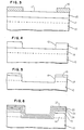
- a window 18 is, as shown in Fig. 4, opened in the oxide layer 15 by using a known etching technique such as chemical etching.
- An ion etching process comprises the introduction of reactive material in vapor form into the chamber with the device to be etched. This vapor is ionized using a plasma so that reactive ions of the reactive material are formed. These ions are then directed against the surface of the device which is to be etched.
- One process for producing such cavities from 0.5 um to 3.0 um deep, with a profile of 85°, using thermal oxide and photoresist as masking material uses a mixture of oxygen O 2 , and dichlorodifluoromethane CCL 2 F 2 , (also known as Freon 12).
- etch rates of the wafer, the oxide and the photoresist, under the above conditions was :
- This technique creates, as shown in Fig. 5, a cavity 19 in the P- epitaxial layer 14 under the oxide window 18.
- the oxide layer 15 should be thick enough that when the cavity 19 extends through the epitaxial layer 14, as shown in Fig. 5, approximately 500 to 1000 A of layer 15 remains on the surface of layer 14. This remaining layer 15 serves as a nucleation barrier for later selective epitaxial silicon deposition.
- the unit is removed from the reactive ion etching apparatus and placed in a chemical vapor deposition (CVD) chamber into which gases containing boron, oxygen and silicon are passed over it
- the unit is maintained in the chamber for a length of time sufficient to create upon the exposed silicon, i.e., the walls and the bottom of the cavity 19 as well as on oxide layer 15 as shown in Fig. 6, a layer of borosilicate glass 20.
- This borosilicate layer 20 may range from 100 A in thickness to 500 A in thickness, and is shown in Fig. 6.
- This borosilicate glass is formed by placing the wafer in the CVD chamber in the presence of silane (SiH4), oxygen (02) and diborane - (B 2 H 6 ).
- the conditions are as follows.
- the temperature of the chamber is raised to about 400°C; the gases are simultaneously introduced at the following flow rates: the silane at 25 to 100 SCCM, the oxygen at 0.25 to 1.0 SLM (Standard Liter per Minute) and the diborane is 10% diborane in nitrogen (N.) at a flow rate of 0.25 to 1.0 SLM; the pressure is maintained at 0.2 to 0.5 Torr; the time is from 10 to 40 minutes.
- the unit is treated with suitable mixtures of silicon, oxygen, and nitrogen to form a suitably thick (100-1000 A) silicon oxynitride layer 21.
- suitable mixtures of silicon, oxygen, and nitrogen to form a suitably thick (100-1000 A) silicon oxynitride layer 21.
- the conditions necessary to create layer 21 are: dichlorosilane SiH 2 Cl 2 at 10 to 50 SCCM is followed into the CVD chamber together with nitrous oxide (N 2 O) and ammonia - (NH,) at 10-70 SCCM for between 10 and 50 minutes while the pressure of the chamber is held between 0.25 and 0.35 Torr and the temperature of the chamber is approximately 825°C.
- gases containing oxygen, silicon and either phosphorus or arsenic are introduced to form a layer 22 of phosphosilicate or arsinosilicate glass on the silicon oxynitride layer.
- This layer will range between 100 and 500 A in thickness.
- phosphosilicate glass is formed by introducing into the CVD chamber silane (SiH4) at 25-100 SCCM together with oxygen (O 2 ) at 0.25-1.0 SLM and 10% phosphine (PH,) in nitrogen (N.) at 0.1-0.75 SLM while maintaining a pressure of 0.2 to 0.5 Torr and a temperature of approximately 400°C.
- arsenosilicate glass instead of the phosphosilicate glass arsine (AsH,) can be substituted for the phosphine. All the other conditions and gases remain the same. Over this glass layer 22 there is now formed a silicon nitride (Si 3 N 4 ) layer 23. Once all these chemical vapor deposition processes are completed the unit is removed from the chamber and placed in a reactive ion chamber. Any suitable reactive ion process, such as the one previously described is performed for a time sufficient to remove the layers 20, 21, 22, and 23 from the bottom of the cavity 19 and top of layer 15 as shown in Fig. 7. This exposes the underlying surface 24 of the substrate 13.
- Any suitable reactive ion process such as the one previously described is performed for a time sufficient to remove the layers 20, 21, 22, and 23 from the bottom of the cavity 19 and top of layer 15 as shown in Fig. 7. This exposes the underlying surface 24 of the substrate 13.
- the reactive ion etching process is a direct line of sight process the effect of it on the layers 20, 21, 22, and 23 on the sides of the cavity 19 are insignificant and for all effects and purposes those layers remain substantially untouched and undiminished in thickness.
- the unit is placed into an oxidizing chamber to form, as shown in Fig. 8, a 200 A to 500 A thick layer 25 of silicon oxide over the surfaces 24 and 15 not protected by Si 3 N 4 . Silicon oxide will not under these conditions form on the surface of the silicon nitride layer 23. This layer 25 effectively heals any damage done to the exposed silicon surface 24. Once this oxide layer 25 is formed it is immediately removed using a suitable buffered hydrofiouride acid etch. This etch must be controlled to leave a significant thickness of layer 15 on the surface of the array while completely exposing surface 24. Following this, the silicon nitride layer 23 is removed from the walls of the cavity by etching with hot phosphoric acid.
- the array is placed into a reduced pressure chemical vapor deposition apparatus and exposed to a silicon containing vapor, such as dichlorosilane or silicon tetrachloride, mixed with an N-type dopant material such as arsenic or phosphorous at a pressure of 80-150 Torr and a temperature of 1050-1150°C.
- a silicon containing vapor such as dichlorosilane or silicon tetrachloride
- an N-type dopant material such as arsenic or phosphorous
- Any excess material formed over and above the surface of the cavity can be easily removed by well known techniques such as a planarization technique.
- the silicon fill material 26 in the pocket makes a good electrical connection with the substrate 11 but remains isolated, by a wall of oxide-nitride 21, from the surrounding P-type epitaxial layer 14 .
- MOS devices typically employ a thick oxide layer 31, is formed over inactive surface areas. Thinner dielectrics 34, usually 150 to 500 A thick, are formed in active device regions. Then, as shown in Fig. 2, two P-type regions 27 and 28 are formed by well known diffusion techniques in the upper surface of the silicon fill material 26. These regions 27 and 28 are each a PN junction with the underlying N-type epitaxial material 26. Similarly, two N-type regions 29 and 30 are formed in layer 14.
- a conductive material typically polycrystalline silicon is then employed to form insulated gates 32 and 33.0ver the respective diffusions 27, 28, 29, and 30 conductive material, i.e., aluminum dots 36, 37, 38, and 39 are then placed to make contact with the respective underlying regions 27, 28, 29, and 30.
- the P channel transistor 11 is thus comprised of pocket 26, gate 32 and region 27 which serves as its source, and region 28 which serves as its drain.
- the N channel transistor 12 is defined by gate 33, and region 29 which serves as its source and region 30 which acts as its drain.
Landscapes
- Element Separation (AREA)
- Metal-Oxide And Bipolar Metal-Oxide Semiconductor Integrated Circuits (AREA)
Applications Claiming Priority (2)
| Application Number | Priority Date | Filing Date | Title |
|---|---|---|---|
| US06/695,716 US4556585A (en) | 1985-01-28 | 1985-01-28 | Vertically isolated complementary transistors |
| US695716 | 1985-01-28 |
Publications (3)
| Publication Number | Publication Date |
|---|---|
| EP0190581A2 true EP0190581A2 (de) | 1986-08-13 |
| EP0190581A3 EP0190581A3 (en) | 1987-08-19 |
| EP0190581B1 EP0190581B1 (de) | 1990-04-11 |
Family
ID=24794198
Family Applications (1)
| Application Number | Title | Priority Date | Filing Date |
|---|---|---|---|
| EP86100564A Expired EP0190581B1 (de) | 1985-01-28 | 1986-01-17 | Senkrecht isolierte komplementäre Transistorstrukturen |
Country Status (5)
| Country | Link |
|---|---|
| US (1) | US4556585A (de) |
| EP (1) | EP0190581B1 (de) |
| JP (1) | JPS61177770A (de) |
| CA (1) | CA1208805A (de) |
| DE (1) | DE3670402D1 (de) |
Cited By (4)
| Publication number | Priority date | Publication date | Assignee | Title |
|---|---|---|---|---|
| DE3700102A1 (de) * | 1987-01-03 | 1988-07-14 | Kallabis Manfred | Schaft einer gelenk-endoprothese |
| WO1989005518A1 (en) * | 1987-12-09 | 1989-06-15 | Ncr Corporation | Process for forming isolation regions in a semiconductor substrate |
| EP0263756A3 (en) * | 1986-10-06 | 1989-09-06 | Fairchild Semiconductor Corporation | Selective epitaxy bicmos process |
| EP0242506A3 (en) * | 1986-03-17 | 1990-03-14 | International Business Machines Corporation | Sidewall spacers for cmos circuits stress relief/isolation and method for making |
Families Citing this family (10)
| Publication number | Priority date | Publication date | Assignee | Title |
|---|---|---|---|---|
| US4728624A (en) * | 1985-10-31 | 1988-03-01 | International Business Machines Corporation | Selective epitaxial growth structure and isolation |
| US4891247A (en) * | 1986-09-15 | 1990-01-02 | Watkins-Johnson Company | Process for borosilicate glass films for multilevel metallization structures in semiconductor devices |
| US4902641A (en) * | 1987-07-31 | 1990-02-20 | Motorola, Inc. | Process for making an inverted silicon-on-insulator semiconductor device having a pedestal structure |
| US4876212A (en) * | 1987-10-01 | 1989-10-24 | Motorola Inc. | Process for fabricating complimentary semiconductor devices having pedestal structures |
| US4925806A (en) * | 1988-03-17 | 1990-05-15 | Northern Telecom Limited | Method for making a doped well in a semiconductor substrate |
| DE3841763A1 (de) * | 1988-12-12 | 1990-06-13 | Basf Ag | Neue tnf-peptide |
| US5234861A (en) * | 1989-06-30 | 1993-08-10 | Honeywell Inc. | Method for forming variable width isolation structures |
| DE4300986C2 (de) * | 1992-01-17 | 1999-08-26 | Mitsubishi Electric Corp | Halbleitervorrichtung zur Elementisolierung und Herstellungsverfahren derselben |
| US5821172A (en) * | 1997-01-06 | 1998-10-13 | Advanced Micro Devices, Inc. | Oxynitride GTE dielectrics using NH3 gas |
| KR20130054010A (ko) * | 2011-11-16 | 2013-05-24 | 삼성전자주식회사 | Iii-v족 물질을 이용한 반도체 소자 및 그 제조방법 |
Family Cites Families (7)
| Publication number | Priority date | Publication date | Assignee | Title |
|---|---|---|---|---|
| US4137109A (en) * | 1976-04-12 | 1979-01-30 | Texas Instruments Incorporated | Selective diffusion and etching method for isolation of integrated logic circuit |
| JPS55160443A (en) * | 1979-05-22 | 1980-12-13 | Semiconductor Res Found | Manufacture of semiconductor integrated circuit device |
| US4476623A (en) * | 1979-10-22 | 1984-10-16 | International Business Machines Corporation | Method of fabricating a bipolar dynamic memory cell |
| US4309716A (en) * | 1979-10-22 | 1982-01-05 | International Business Machines Corporation | Bipolar dynamic memory cell |
| JPS58192346A (ja) * | 1982-05-06 | 1983-11-09 | Toshiba Corp | 半導体装置の製造方法 |
| JPS58197871A (ja) * | 1982-05-14 | 1983-11-17 | Toshiba Corp | 半導体装置およびその製造方法 |
| JPS5919347A (ja) * | 1982-07-23 | 1984-01-31 | Matsushita Electric Ind Co Ltd | 半導体集積回路およびその製造方法 |
-
1985
- 1985-01-28 US US06/695,716 patent/US4556585A/en not_active Expired - Fee Related
- 1985-05-21 CA CA000481991A patent/CA1208805A/en not_active Expired
- 1985-10-15 JP JP60227932A patent/JPS61177770A/ja active Pending
-
1986
- 1986-01-17 EP EP86100564A patent/EP0190581B1/de not_active Expired
- 1986-01-17 DE DE8686100564T patent/DE3670402D1/de not_active Expired - Lifetime
Cited By (4)
| Publication number | Priority date | Publication date | Assignee | Title |
|---|---|---|---|---|
| EP0242506A3 (en) * | 1986-03-17 | 1990-03-14 | International Business Machines Corporation | Sidewall spacers for cmos circuits stress relief/isolation and method for making |
| EP0263756A3 (en) * | 1986-10-06 | 1989-09-06 | Fairchild Semiconductor Corporation | Selective epitaxy bicmos process |
| DE3700102A1 (de) * | 1987-01-03 | 1988-07-14 | Kallabis Manfred | Schaft einer gelenk-endoprothese |
| WO1989005518A1 (en) * | 1987-12-09 | 1989-06-15 | Ncr Corporation | Process for forming isolation regions in a semiconductor substrate |
Also Published As
| Publication number | Publication date |
|---|---|
| JPS61177770A (ja) | 1986-08-09 |
| CA1208805A (en) | 1986-07-29 |
| US4556585A (en) | 1985-12-03 |
| EP0190581B1 (de) | 1990-04-11 |
| DE3670402D1 (de) | 1990-05-17 |
| EP0190581A3 (en) | 1987-08-19 |
Similar Documents
| Publication | Publication Date | Title |
|---|---|---|
| US4356211A (en) | Forming air-dielectric isolation regions in a monocrystalline silicon substrate by differential oxidation of polysilicon | |
| KR100384761B1 (ko) | N2o 질화 산화물 트렌치 측벽과 절연구조를 형성하는 방법 | |
| US4530149A (en) | Method for fabricating a self-aligned vertical IGFET | |
| US5304510A (en) | Method of manufacturing a multilayered metallization structure in which the conductive layer and insulating layer are selectively deposited | |
| US5700712A (en) | Method for manufacturing an insulating trench in an SOI substrate for smartpower technologies | |
| EP0363944B1 (de) | Verfahren zur Herstellung eines Halbleiterbauelementes, das eine Siliciumcarbidschicht besitzt | |
| US5401998A (en) | Trench isolation using doped sidewalls | |
| KR100227766B1 (ko) | 반도체 장치 및 그 제조 방법 | |
| US5436190A (en) | Method for fabricating semiconductor device isolation using double oxide spacers | |
| EP0190581B1 (de) | Senkrecht isolierte komplementäre Transistorstrukturen | |
| KR20010063781A (ko) | 반도체소자의 제조방법 | |
| EP0147913B1 (de) | Verfahren zur Herstellung einer Halbleiteranordnung mittels einer selektiven Dampfphasenanwuchstechnik | |
| US4900689A (en) | Method of fabrication of isolated islands for complementary bipolar devices | |
| US4716451A (en) | Semiconductor device with internal gettering region | |
| US5525535A (en) | Method for making doped well and field regions on semiconductor substrates for field effect transistors using liquid phase deposition of oxides | |
| US4965219A (en) | Method for the manufacturing of insulated gate field effect transistors (IGFETS) having a high response speed in high density integrated circuits | |
| US6445043B1 (en) | Isolated regions in an integrated circuit | |
| KR20040025967A (ko) | 선택적 에피택셜 성장법을 이용한 콘택플러그를 갖는반도체소자 및 그의 제조 방법 | |
| US6303496B1 (en) | Methods of filling constrained spaces with insulating materials and/or of forming contact holes and/or contacts in an integrated circuit | |
| KR100524802B1 (ko) | 이중 선택적 에피택셜 성장법을 이용한 콘택플러그를 갖는반도체소자 및 그의 제조 방법 | |
| US5234863A (en) | Method of manufacturing doped contacts to semiconductor devices | |
| JPH0945900A (ja) | Mis型fetおよびその製造方法 | |
| KR100440078B1 (ko) | 반도체소자의 제조방법 | |
| JPS6155250B2 (de) | ||
| US6309939B1 (en) | Method of manufacturing a semiconductor device |
Legal Events
| Date | Code | Title | Description |
|---|---|---|---|
| PUAI | Public reference made under article 153(3) epc to a published international application that has entered the european phase |
Free format text: ORIGINAL CODE: 0009012 |
|
| AK | Designated contracting states |
Kind code of ref document: A2 Designated state(s): DE FR GB IT |
|
| 17P | Request for examination filed |
Effective date: 19861125 |
|
| PUAL | Search report despatched |
Free format text: ORIGINAL CODE: 0009013 |
|
| AK | Designated contracting states |
Kind code of ref document: A3 Designated state(s): DE FR GB IT |
|
| 17Q | First examination report despatched |
Effective date: 19890228 |
|
| GRAA | (expected) grant |
Free format text: ORIGINAL CODE: 0009210 |
|
| AK | Designated contracting states |
Kind code of ref document: B1 Designated state(s): DE FR GB IT |
|
| PG25 | Lapsed in a contracting state [announced via postgrant information from national office to epo] |
Ref country code: IT Free format text: LAPSE BECAUSE OF FAILURE TO SUBMIT A TRANSLATION OF THE DESCRIPTION OR TO PAY THE FEE WITHIN THE PRESCRIBED TIME-LIMIT;WARNING: LAPSES OF ITALIAN PATENTS WITH EFFECTIVE DATE BEFORE 2007 MAY HAVE OCCURRED AT ANY TIME BEFORE 2007. THE CORRECT EFFECTIVE DATE MAY BE DIFFERENT FROM THE ONE RECORDED. Effective date: 19900411 |
|
| REF | Corresponds to: |
Ref document number: 3670402 Country of ref document: DE Date of ref document: 19900517 |
|
| ET | Fr: translation filed | ||
| PLBE | No opposition filed within time limit |
Free format text: ORIGINAL CODE: 0009261 |
|
| STAA | Information on the status of an ep patent application or granted ep patent |
Free format text: STATUS: NO OPPOSITION FILED WITHIN TIME LIMIT |
|
| 26N | No opposition filed | ||
| PGFP | Annual fee paid to national office [announced via postgrant information from national office to epo] |
Ref country code: GB Payment date: 19951215 Year of fee payment: 11 |
|
| PGFP | Annual fee paid to national office [announced via postgrant information from national office to epo] |
Ref country code: FR Payment date: 19960103 Year of fee payment: 11 |
|
| PGFP | Annual fee paid to national office [announced via postgrant information from national office to epo] |
Ref country code: DE Payment date: 19960126 Year of fee payment: 11 |
|
| PG25 | Lapsed in a contracting state [announced via postgrant information from national office to epo] |
Ref country code: GB Effective date: 19970117 |
|
| GBPC | Gb: european patent ceased through non-payment of renewal fee |
Effective date: 19970117 |
|
| PG25 | Lapsed in a contracting state [announced via postgrant information from national office to epo] |
Ref country code: FR Effective date: 19970930 |
|
| PG25 | Lapsed in a contracting state [announced via postgrant information from national office to epo] |
Ref country code: DE Effective date: 19971001 |
|
| REG | Reference to a national code |
Ref country code: FR Ref legal event code: ST |