EP0190813A2 - Verarbeitungszelle für fehlertolerante Matrixanordnungen - Google Patents
Verarbeitungszelle für fehlertolerante Matrixanordnungen Download PDFInfo
- Publication number
- EP0190813A2 EP0190813A2 EP86300018A EP86300018A EP0190813A2 EP 0190813 A2 EP0190813 A2 EP 0190813A2 EP 86300018 A EP86300018 A EP 86300018A EP 86300018 A EP86300018 A EP 86300018A EP 0190813 A2 EP0190813 A2 EP 0190813A2
- Authority
- EP
- European Patent Office
- Prior art keywords
- cell
- input
- processor
- output
- array
- Prior art date
- Legal status (The legal status is an assumption and is not a legal conclusion. Google has not performed a legal analysis and makes no representation as to the accuracy of the status listed.)
- Granted
Links
Images


Classifications
-
- G—PHYSICS
- G11—INFORMATION STORAGE
- G11C—STATIC STORES
- G11C29/00—Checking stores for correct operation ; Subsequent repair; Testing stores during standby or offline operation
- G11C29/006—Checking stores for correct operation ; Subsequent repair; Testing stores during standby or offline operation at wafer scale level, i.e. wafer scale integration [WSI]
-
- G—PHYSICS
- G06—COMPUTING OR CALCULATING; COUNTING
- G06F—ELECTRIC DIGITAL DATA PROCESSING
- G06F15/00—Digital computers in general; Data processing equipment in general
- G06F15/76—Architectures of general purpose stored program computers
- G06F15/80—Architectures of general purpose stored program computers comprising an array of processing units with common control, e.g. single instruction multiple data processors
- G06F15/8007—Architectures of general purpose stored program computers comprising an array of processing units with common control, e.g. single instruction multiple data processors single instruction multiple data [SIMD] multiprocessors
- G06F15/8023—Two dimensional arrays, e.g. mesh, torus
-
- G—PHYSICS
- G06—COMPUTING OR CALCULATING; COUNTING
- G06F—ELECTRIC DIGITAL DATA PROCESSING
- G06F11/00—Error detection; Error correction; Monitoring
- G06F11/22—Detection or location of defective computer hardware by testing during standby operation or during idle time, e.g. start-up testing
- G06F11/26—Functional testing
- G06F11/267—Reconfiguring circuits for testing, e.g. LSSD, partitioning
Definitions
- This invention relates to a processing cell for fault tolerant arrays, ie the cell is intended as a building block for use in constructing fault-tolerant arrays of processing cells.
- United States Patent No 3913072 describes the formation of a fully operational one-dimensional or linear array of ICs from a partly faulty two-dimensional wafer-scale array. A viable IC is first selected and connections are made to a further viable IC selected from four nearest neighbours. IC testing is carried out from an off- wafer source. The procedure is carried out until a chain of ICs of the required length is built up. The circuitry for IC testing, selection and connection is complex. Furthermore, the procedure is only capable of providing a one-dimensional array of ICs in series.
- the present invention provides a processing cell for use in constructing fault tolerant cell arrays, the cell including:-
- the processing cell of the invention is intended for use as a building block in constructing fault-tolerant cell arrays. It provides the advantage that a cell is arranged to be operationally included within an array if and only if it has a fault-free processor and it receives input request and availability signals indicating that neighbouring cells are available for connection to it. The cell also generates its own availability and request signals for transmission to neighbouring cells indicating routes available for signal transmission through the array. It achieves this without reference to or need for any external test or control circuits.
- the cell implementing means is arranged to operate a priority scheme in which use of each of the second input and output signal lines is preferred to use of the respective third, and use of each of the first input and output signal lines is preferred to use of the respective second.
- the cell may include a further input line and a further output line, these being arranged either to route additional signals to and from the processor or to bypass it in accordance with whether or not the processor is fault-free.
- This arrangement makes provision for signal transmission in an additional direction through a cell array, the direction being functionally orthogonal to that previously indicated.
- An array of processing cells of the invention may be arranged in combination with an array of input cells and an array of output cells.
- the input cell array is arranged to configure input to the processing cell array such that only operational rows of processing cells receive processor input signals.
- the output cell array is arranged to configure outputs from the array such that only operational rows of processing cells are addressed to provide output signals.
- One of the input and output cell arrays may be provided with means arranged to indicate whether or not a predetermined minimum number of operational rows of processing cells is available.
- the cells of the invention may be arranged to be suitable for forming an array which is reconfigurable in two dimensions, ie an array having variable numbers of both rows and columns.
- the invention would be arranged to avoid double site and improper crossover problems to be described.
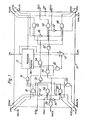
- the cell 10 has twenty input/output terminals having references with a prefix IP, OP, REQ, or AVAIL and a suffix N, S, E, W, NE, NW, SE or SW.
- the prefixes represent input, output, request and available respectively, and the suffixes are points of the compass indicating the relevant location.
- "AVAILNE” for example represent "available North East”. This reference scheme assists circuit analysis, as will be described.
- Terminal IPN is connected to a processor 12 and a 0-selected input of a two-input multiplexer 14.
- the output of multiplexer 14 is connected to OPS terminal.
- IPNW and REQNW terminals are connected to the two inputs of an AND gate 16, the output of this gate providing one input to a three-input OR gate 18.
- the processor 12 receives the output of OR gate 18.
- REQNW terminal is also connected directly as input to a three-input OR gate 20, and via an inverter 22 as input to three-input AND gates 24 and 26 and two- and four-input AND gates 28 and 30.
- REQW terminal is connected directly as input to OR gate 20 and AND gate 26, and via an inverter 32 as input to AND gates 24 and 30.
- IPW terminal provides a third input to AND gate 26.
- REQSW and IPSW terminals provide third and fourth inputs to AND gate 30, and the former also provides a third input to OR gate 20.
- the outputs of AND gates 26 and 30 provide second and third inputs to OR gate 18.
- OR gate 20 is connected to one input of a two-input AND gate 34, which receives a second input from a PASS/FAIL section 36 of processor 12.
- the section 36 furnishes a 0 output if processor 12 is faulty and 1 otherwise.
- AND gate 38 providing output to the AVAILNW terminal, to the third input of AND gate 24, to the second input of AND gate 28 and to a first input of a further AND gate 40:
- OR gate 20 output provides a second input to AND gate 40, whose output controls input line selection by multiplexer 14 for subsequent output.
- AVAILSW and AVAILW terminals are connected to the outputs of AND gates 24 and 28 respectively.
- AND gate 34 output provides first inputs to two-, three- and four-input AND gates 42, 44 and 46.
- AVAILNE terminal is connected to a second input of AND gate 42, to an inverter 48 providing inputs to AND gates 44 and 46, and to a first input of a three input OR gate 50.
- the output of OR gate 50 is connected to a second input of AND gate 38.
- AVAILE terminal is connected to a third input of AND gate 44, to a second input of OR gate 50, and to an inverter 52 providing a third input to AND gate 46.
- AVAILSE terminal is connected to a fourth input of AND gate 46 and to a third input of OR gate 50.
- REQNE, REQE and REQSE terminals are connected to the outputs of AND gates 42, 44 and 46 respectively.
- OPNE, OPE and OPSE are connected directly to processor 12.
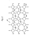
- FIGS. 2 and 3 respectively show rectangular arrays 60 and 62 of processors such as 64 and 64' illustrated schematically as circles.
- the arrays 60 and 62 have northern and western inputs N and W, and southern and eastern outputs S and E.
- the array 60 has three rows and five columns of processors such as 64 these having North, South, East and West (N,S, E and W) nearest-neighbour interconnections as indicated by lines such as 66.
- Array 62 has four rows and five columns of processors 64', some of which are faulty as indicated by crosses thereon such as 64'.
- processor interconnections such as 68 are in the N, S, E or W directions, but there are also bypass connections such as 70 around faulty or unwanted cells.
- bypass connections such as 70 around faulty or unwanted cells.
- SE/NW and NE/SW interconnections 72 and 74 there are oblique or SE/NW and NE/SW interconnections 72 and 74.
- Array 60 represents an array of perfect or fully operational cells arranged in combination to carry out a digital signal processing operation. It corresponds to a manufacturing procedure in which all faulty devices are discarded, resulting in unacceptably low yields. In fact, as processor complexity and array size increases yields rapidly become effectively zero. This is a major problem facing the development of wafer-scale integrated circuits in particular.
- array 62 Compared to array 60, array 62 has an extra row of cells 64'. This enables faulty and unwanted cells to be bypassed as indicated at 70.. Those cells in the array 62 which have connections to neighbours can be seen to form a three by five array functionally equivalent to array 60.
- the cell 10 is designed to form an array building block, so that reconfigured arrays can be formed equivalent to perfect arrays.
- Each cell 10 is arranged to communicate with one eastern and one western neighbour selected from up to three of each which would be present in an array of cells 10. Such an array would be reconfigurable as indicated in Figure 3 to bypass faulty and unwanted cells.
- the cell 10 receives up to three request signals (REQNW, REQW and REQSW) from western neighbours, and up to three availability signals (AVAILNE, AVAILE and AVAILSE) from eastern neighbours. It provides a request signal (REQNE, REQE or REQSE) to one of three eastern neighbours, and receives up to three availability signals from western neighbours.
- the cell 10 must only output a true (logic 1) availability signal if it has a fault-free processor 12, and at least one of its eastern neighbours is outputting a true availability signal to it. If this is satisfied, a priority system is implemented by the cell 10 to decide in which western direction the cell itself will output a true availability signal.
- the priority system is set out in Table 1 below, in which true, false and X respectively represent logic 1, 0 and either 1 or 0 (true or false) arbitrarily.
- the Table 1 scheme establishes a hierarchy of NW, W and SW in descending order of priority as regards availability for connection of the cell 10 thereto.
- the cell must be available for connection to an NW neighbour on receipt of a true REQNW signal, irrespective of W and SW request signals. It must be available for connection to a W neighbour in response to a request therefrom, provided that no NW true request is received and irrespective of any REQSW signal. It must be available to an SW neighbour in the event that both REQNW and REQW are false.
- the cell 10 should also remain available to all three neighbours when all request inputs are false.
- the cell 10 implements as follows the Table 1 priority scheme and the requirement that any availability is conditional on a fault-free processor 10 combined with receipt of a true availability signal from an eastern neighbour.
- OR gate 50 receives input of all three eastern availability signals AVAILNE, AVAILE and AVAILSE. If any of these is true, OR gate 50 outpus 1 to AND gate 38, which in turn outputs 1 provided that PASS/FAIL section 36 of processor 12 outputs 1 indicating a fault-free state.
- the output of AND gate 38 appears directly at AVAILNW terminal, and is fed to AND gates 28 and 24 providing AVAILW and AVAILSW.
- the cell -10 is actually implemented, as opposed to being available, only if it receives a request signal from the west.
- Western input to processor 12 is via OR gate 18, which receives input from AND gates 16, 26 and 30.
- a 1 or true signal from REQNW terminal provides a 1 input to AND gate 16, but 0 inputs to AND gates 26 and 30.
- OR gate 18 accordingly receives 0 inputs from AND gates 36 and 30 irrespective of the IPW, REQW, IPSW and REQSW signals.
- the output of AND gate 16, and so also that of OR gate 18 to processor 12, will be 0 or 1 in accordance with signal IPNW being 0 or 1. This effectively inputs IPNW to processor 12. If REQNW is 0, inverter 22 supplies a 1 input to AND gates 26 and 30.
- AND gate 26 receives a second 1 input but inverter 32 provides a 0 to AND gate 30.
- OR gate 18 accordingly receives 0 inputs from AND gates 16 and 30, and 0 or 1 from AND gate 26 according to 0 or 1 IPW signals. This effectively inputs IPW to processor 12.
- inverters 22 and 32 provide respective 1 inputs to AND gate 30.
- a third 1 input is received by this gate if REQSW is true; its output to OR gate 18 and thence to processor 12 will be 0 or 1 according 0 or 1 at its fourth input from IPSW terminal.
- Request signals are generated by (as opposed to input to) the cell 1 0 for output to eastern neighbours in accordance with a different scheme.
- the cell must only output a true request signal if processor 12 is fault-free and at least one western neighbour provides a true input request signal. If this condition is satisfied, the cell outputs a single true request to the east in accordance with the priority scheme of Table 2 below, which incorporates Table 1 nomenclature.
- an AVAILNE input signal produces a REQNE output irrespective of availability inputs from E or SE.
- AVAILNE is false
- a true AVAILE produces a true REQE irrespective of AVAILSE.
- an AVAILSE true signal produces a true REQSE.
- all input availability signals are false
- all output request signals are false. This establishes NE, E and SE in descending order of priority for connection to the cell.
- the hierarchical structure is similar to that for connection to western neighbours.
- the cell 10 implements as follows the Table 2 priority scheme and the requirement that processor 12 be fault-free combined with receipt of a true western request signal.
- OR gate 20 receives all three western availability signals. If any of these is true, OR gate 20 outputs 1 to AND gate 34, which in turn outputs 0 or 1 to AND gates 42, 44 and 46 according to whether or not processor 12 is faulty. Accordingly, all eastern request outputs are 0 or false if there is no western neighbour available or processor 12 is faulty. If AND gate 34 output is 1, the following applies.
- AND gate 42 receives AVAILNE directly, whereas AND gates 44 and 46 receive it after inversion at 48. A true AVAILNE accordingly provides for 1, 0 and 0 to be input to AND gates 42, 44 and 46 respectively.
- AND gates 44 and 46 then output 0 or false to REQE and REQSE terminals, whereas AND gate 42 provides a true output to REQNE terminal. If AVAILNE is false, AND gates 44 and 46 receive 1 inputs from inverter 48 together with 1 inputs from AND gate 34.
- AND gate 44 receives all true inputs and provides a true output at REQE terminal.
- a true AVAILE signal is however inverted at 52, which provides a false signal input to AND gate 46 and consequent false output at REQSE terminal. If AVAILNE and AVAILE signals are both false but AVAILSE is true, AND gate 46 receives all true inputs and provides a true REQSE output. If all three eastern availability signals are false, all eastern request signals are false.
- AND gate 40 provides for the processor 12 to be implemented or bypassed according to whether or not the cell 10 is both east-west connectable and the processor 12 is fault-free.
- AND gate 40 receives inputs from OR gate 20 and AND gate 38, both being true if there are east and west neighbours generating true availability and request signals respectively and processor 12 is fault-free.
- AND gate 40 output is then 1, and multiplexer 14 routes its I-selected input or processor 12 output signal to OPS terminal. If AND gate 40 output is 0, multiplexer 14 connects IPN through to OPS bypassing processor 12.
- the cell 10 has inputs and outputs arranged for bit-serial signals
- adaptation to deal with bit-parallel signals is straightforward.
- IPW consisted of n terminals for connection to an n-bit bus
- n AND gates 26 could be employed in parallel to provide one gate per input bit. Similar arrangements would be required at other non-REQ western inputs, and multiplexer 14 would be replicated. Outputs other than REQ or AVAIL would only require buses to replace one-bit lines.
- the invention has been described in terms of a cell 10 connectable to N, S, E and W neighbours to form part of the functional equivalent of a rectangular array. However,it may also form part of a linear array in which only East-West connections are required. In this case it is unnecessary to provide IPN and OPS terminals, AND gate 40 and multiplexer 14. Such a cell may then be arranged in a three row array from which a single functional row would be obtainable. For lower but still some fault tolerance, the cell could be part of a two row array. In this case it would not be necessary to arrange for a priority scheme to govern cell connection, since only selection between one of two alternatives would be required to avoid connection of both alternatives. A priority scheme would however both implement this and provide for use of a previously idle cell in the event of in-service cell failure.
- processor 12 in the cell 10. This is because such arrangements are known in the art, as described for example by D Komonytsky in "LSI Self Test using LSSD and Signature Analysis, IEEE Test Conference 1982.
- the processor itself may be a microprocessor, a transputer or part of a distributed array processor.
- the form of processor 12 may of course differ between different cells 10 in an array.
- An array of cells 10 configured in accordance with Figure 3 provides three functional rows out of four. Column inputs and outputs to N and from S respectively remain fixed, since the number of columns in the array does not change. However, row input and output connections to W and from E respectively are not predetermined. These will vary from array to array depending on which rows are operational. Moreover, they may change during array operation if a processor 12 fails in service, and the array is reconfigured as a result. From the previous description, it will be apparent that a fully operational row will always begin with a west array edge cell which has a true AVAILW output. Input to such a cell may therefore be made to the cell's IPW terminal. Furthermore, any cell at the end of a fully operational row provides a true REQE output.
- the input cell 80 for forming an input array as will be described.
- the input cell 80 has a NS line 82 connecting IPN and OPS signal terminals, and an EW line 84 connecting IPW and OPE signal terminals.
- An IPN control (CTRL) input is connected by an NS CTRL line 86 as input to a NAND gate 88 and an AND gate 90.
- the output of AND gate 90 is fed to an OPS CTRL output.
- An AVAILE input is connected both to NAND gate 88 and to a second AND gate 92, the output of the latter being fed to an AVAILW output.
- NAND gate 88 output is fed as a respective second input to each of AND gates 90 and 92. This output is also inverted at 94 and used to control a transistor switch 96 connected between lines 82 and 84.
- REQW and REQE terminals are connected directly together by an EW line 98.
- the cell 80 operates as follows. If it receives true AVAILE and IPN CTRL signals, NAND gate 88 produces a 0 output. This is inverted to 1 by inverter 94, and switch 96 is switched on connecting IPN to OPE via lines 82 and 84. Moreover, AND gates 90 and 92 receive NAND gate 88's 0 output, and produce 0 outputs at CTRL OPS and AVAILW. If either AVAILE or IPN CTRL receives 0, IPN is not connected to REQE and AND gates 90 and 92 receive 1 from NAND gate 88. AVAILW then becomes 0 or 1 according to whether AVAILE is 0 or 1, and CTRL OPS becomes 0 or 1 according to whether IPN CTRL is 0 or 1. The function of REQW and REQE will be described later.
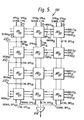
- FIG. 5 there is shown an input array 100 of three columns and four rows of input cells 80.
- Features not specifically referred to are unreferenced and undrawn to avoid unnecessary figure complexity.
- Each input cell 80 has inputs and outputs connected to neighbouring cells (where available) as shown.
- East column cells 80 20 to 80 23 have AVAILE, OPE and REQE terminals for connetion to the western edge terminals of five column, four row array of cells 10 (not shown), as described with reference to Figures 1 and 3.
- REQW terminal receives a permanent 1 or true input signal, as do all top row CTRL terminals IPN 00 to IPN 20 .
- CTRL OPS 00 is connected to REQW 01 by a line 102 0 , and similarly lines 102 1 and 102 2 connect CTRL OPS 01 and CTRL OPS 02 to REQW 02 and REQW 03 respectively.
- Bottom row cell SIGNAL OPS terminals are all unconnected, but the corresponding CTRL OPS terminals are all connected as inputs to a three input NOR gate 104.
- the array 100 operates as follows. IPN 00 to IPN 20 terminals provide three signal inputs for three operational rows of a four row array of cells 10, some of which are faulty as shown in Figure 3. Input is to be made to IPW terminals of cells 10 of a western edge array column provided that each cell begins an operational row.
- IPN 20 CTRL is 1, and REQE 20 is 1 because REQE 00 is 1, IPN 20 is connected or unconnected to the adjacent array (not shown) via OPE 20 according to whether AVAILE 20 is 1 or 0 indicating an operational row of cells 10. This follows directly from the function of cells 80 as previously described.
- CTRL OPS 20 receives 0 from AND gate 90 20 (see Figure 4); this signal passes through cells 80 21 , 80 22 and 80 23 as successive CTRL input and output signals before reaching CTRL OPS 23 and NOR gate 104. This ensures that IPN 20 cannot subsequently be connected to any of OPE 21 to OPE 23 after connection to OPE 20 . Connection of IPN 20 to OPE 20 is accompanied by a 0 appearing at AVAILW 20 , and consequently at AVAILE 10 and AVAILE 00 also. This ensures that IPN 10 is not connected to OPE 10 and thence to OPE 20 .
- IPN 10 signals pass to cell 80 11 , which also receives a 1 from CTRL OPS 10 indicating non-connection of IPN 10 to OPE 10 . If AVAILE 21 is 1, then since its CTRL input signal is 0 cell 80 21 provides an AVAILW output signal of 1. This becomes the AVAILE input signal to cell 80 11 , which responds by connecting its IPN 11 to OPE 11 . A through connection is accordingly provided from IPN 10 to OPE 21 via IPN 11 and OPE 11 of cell 80 11 . In addition, 0 CTRL signals pass to cells 80 12 and 80 13 for output at CTRL OPS 13 , and a 0 AVAIL signal passes to cell 80 01 . IPN 10 accordingly cannot subsequently become connected to OPE 22 or OPE 23 .
- CTRL 00 is 1 and so also is REQW 01 connected thereto. Connection of IPN 10 to OPE 21 is therefore accompanied by a true REQ 21 output signal, ensuring connection of OPE 21 to an operational row of the adjacent array (not shown) to the east of array 100.
- CTRL OPS 03 receives a 1 signal indicating that an EW line 98 is still being sought.
- the output from NOR gate 104 accordingly is 0, indicating an array of cells 10 which is non-operational since it has insufficient rows available.
- FIG. 6 there is shown an output cell 180 similar to input cell 80, but arranged to reconfigure outputs from an array of cells 10 in accordance with operational row availability.
- the output cell 180 is virtually a mirror image or lateral inversion of cell 80; for this reason equivalent features are like-referenced with the prefix 100.
- the differences are that: (1) there is no equivalent of REQW-REQE line 98; (2) REQW terminal is connected to AND gate 192 and thence to REQE terminal, rather than the AVAILE-AND gate 92-AVAILW connection; and (3) signals pass from terminals IPW or IPS to OPN SIGNAL terminal upwardly, rather than downwardly as before.
- output cell 180 is analogous to that of input cell 80.
- IPN CTRL and REQW signals which are both 1 result in transistor switch 196 connecting IPW to line 182 between IPN and OPS signal terminals. If either of these two signals is 0, both REQE and CTRL OPS terminals receive 0. Since operation is very similar to that set out with reference to Figure 4, a detailed analysis will not be given. -
- FIG. 7 there is shown an output array 200 of three columns and four rows of output cells 180.
- Features not specifically referred to are unreferenced and undrawn to avoid unnecessary figure complexity.
- Each output cell 180 has respective inputs and outputs connected to its N, S, E and W neighbours (where available) as appropriate.
- Each west or left-hand column cell 180 0j has respective REQW 0j and IPW Oj terminals connected to respective REQE 0j and OPEOj terminals of a cell 10 in an extreme right-hand or east column of an array of cells 10 (not shown); ie the output array 200 receives the output of an array of cells 10 equivalent to array 62 of Figure 3.
- Control signals permanently set to 1 are applied to top row IPN iO CTRL terminals.
- connections IPW 00 - OPN 00 SIGNAL, IPW 01 - OPN10 SIGNAL and IPW 02 - OPN 20 SIGNAL become established via cells 180 00 - 180 01 - 18 0 11 - 18010 and 180 02 - 180 12 - 180 22 - 18021 - 180 20 respectively.
- IPW 03 is left unconnected to any OPN SIGNAL irrespective of the associated REQW 03 terminal input signal.
- IPW 00 is not connected to OPN 00 or any other top row cell output. If in addition REQW 01 to REQW 03 terminals receive true input signals, IPW 01 to IPW 03 become connected to OPN 00 to OPN02 respectively via cells 180 01 - 180 00 , 180 02 - 180 12 - 180 11 - 180 10 and 180 03 - 180 13 - 180 23 - 180 22 - 180 21 - 180 20 .
- This analysis extends naturally so that for one false REQW input signal, OPN 00 to OPN 02 become connected to the remaining three of IPW 00 to IPW 03 associated with respective true REQW input signals.
- REQW 00 to REQW 03 terminals receive false input signals, there are fewer operational rows of cells 10 (not shown) available than are required for connection of OPN 00 to OPN 20 .
- NOR gate 104 in Figure 5 would indicate a non-operational array of cells 10. It is also possible to NOR together the CTRL OPS terminals (not shown) of bottom row cells 180 03 to 180 23 to provide a functional state indication.
- control inputs (IPN) to top row cells 80 and 180 were uniformly initialised to 1. It is however possible to employ these inputs to provide array size programmability.
- a processing array of cells 10 having m columns and n rows, m and n being arbitrary positive integers equal to at least 3 for most applications.
- the number of rows n defines the maximum number of inputs to and outputs from the processing array when all cells 10 are operational.
- Such an array might be a wafer-scale integrated circuit (IC) array of transputer processors 12 within cells 10 together with input and output arrays similar to arrays 100 and 200. Individual applications of the IC array might require k functional rows where 1 ⁇ k ⁇ n.
- processor 12 may have in the order of or more than 10 4 gates.
- the additional gate count in a cell 10 is only about 20. (The gate count depends on how complex each circuit is, as well as how many circuits there are.
- Four-input AND gate 30 or 46 might be counted as two or more gates).
- input/output arrays such as 100/200 add only five gates per cell 80 and 180, treating inverters and transistor switches as gates.
- the overhead is 520 gates. This is designed to achieve an operational processing array functionally equivalent to array 60 having fifteen operational processors 64, which would have a total number of gates in the order of 1.5 x 10 . An array 62 would have in the order of 2 x 10 gates.
- the overhead of 520 gates represents only an extra 0.25X in 2 x 10 5 gates, and faults in these additiona circuits can be ignored for practical purposes.
- the illustrated embodiment relates to an array 62 in which each row extends over the full array width. Fault tolerance is achieved in effect by reducing the number of array rows, with the number of columns remaining constant.
- the array 62 may be considered as a full width, variable height array. It will be apparent that a variable width, full height array can be formed by rotating the array 62 through 90°. This produces a constant row, variable column array. In either case, the array is reconfigurable in one dimension only. For some purposes it may be desirable to form arrays which are reconfigurable in two dimensions.
- FIG. 8 there is illustrated what is herein referred to as the "double site" condition.
- An array 220 is shown comprising individual cells represented by circles such as 222. Cells not connected are indicated by overwritten crosses such as 224. Operational rows and columns are indicated by continuous and chain lines 226 and 228 respectively.
- ellipses 230 there are several instances of an adjacent pair of cells occupying both the same respective row and column; ie a column contains two cells of a row (or vice versa), which conflicts with the array requirement that rows and columns should cross at single processor sites.
- This problem is avoided by arranging each cell to become bypassed in both row and column in the event that it is in a state requesting connection to an SE or SW neighbour for both row and column connection purposes. This bypasses the upper of a double site pair of cells, and is preferred. The lower could of course be bypassed by substituting NE/NW for SE/SW in the foregoing.
- FIG. 9(a) and 9(b) there is illustrated a further difficulty referred to herein as an improper crossover.
- Four cells 240a 1 to 240a4 and 240b 1 to 240b 4 are shown with row connections 242a and 242b in solid lines and column connections 244a and 244b in chain lines.
- improper crossovers occur because a row/column intersection does not occur at a cell site.
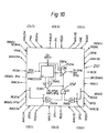
- Figure 10 shows a cell 250 of the invention with an interconnection scheme appropriate for connection as part of a two dimensionally reconfigurable array.
- the cell 250 is equivalent to a combination of two cells 10 ( Figure 1) with a 90° relative rotation; however, the two equivalents of AND gate 40 controlling processor implement/bypass multiplexer 14 are omitted.
- Figure 10 only that circuitry differing from the combination of two cells 10 will be described, since in all other respects it operates precisely in row and column reconfiguration as cell 10 does for row reconfiguration.
- the cell 250 has as illustrated twice the number of input/output connections and twice the internal circuitry (not shown) as the cell 10, apart from omitted AND gate 40. It accordingly provides for request, availability and input/output signals for both row and coluums reconfiguration. It includes two processor implement/bypass multiplexers 252EW and 252NS. These multiplexers are both input-selected 'Y the output from an OR gate 254 having two inputs provided by AND gates 256SE and 256SW.
- AND gate 256SE has input signals provided by REQSE output signals for both rows and columns.
- the inputs to AND gate 256SW are the REQSW (Rows) input signal and REQSW (Cols) output signal.
- Gate 256SE ANDs the row and column REQSE output signals; if both signals are 1, indicating requests for both row and column connection to an SE neighbour, the double site condition has occurred and OR gate 254 receives a 1 input. A 1 signal accordingly reaches both multiplexers 252EW and 252NW, so that their processor bypass inputs 258EW and 258NS are connected respectively to eastern and southern outputs. Similarly, if the REQSW (Rows) input and REQSW (Cols) output signals are both 1, indicating attempted row and column connection to an SW neighbour, AND gate 256SW outputs 1 to OR gate 254 and multiplexer bypass both NS and EW is implemented once more.
- processor bypass by multiplexer means in the event of processor failure such as the AND gate 40/nultiplexer 14 arrangement of cell 10, is not required.
- output request and availability signals are controlled to both eastern and southern neighbours by processor state, so these signals provide for bypass in both directions without further circuitry. It will be noted that the double site condition is avoided in cell 250 with the use of only three additional gates.
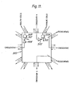
- FIG. 11 there is shown a processing cell 300 equivalent to cell 250 of Figure 10 with additional circuitry to avoid improper crossovers.
- the cell 300 has two additional inputs, crossover N and Crossover W, and also two additional outputs, Crossover E and Crossover S.
- Crossover N and W inputs are connected to inverters 302 and 304 having outputs fed to respective AND gates 306 and 308.
- the inverter outputs are ANDed with signals at 310 and 312 which in cell 250 would have been the AVAILNW (Columns) and AVAILNE (Columns) signals respectively. This provides new AVAIL signals in the corresponding directions.
- Crossover E and S outputs are connected REQNE (Rows) and REQNE (Rows) respectively.
- the cell 300 operates as follows. In an array, a bit is passed from cell to cell 300 in both the NS and WE directions.
- the NS.direction input bit indicates whether or not a northern neighbour cell is outputting a row request in the SE direction; if so, the AVAILNE (Cols) signal for a southern neighbour cell is caused to be inhibited. This avoids the Figure 9(a) condition.
- the WE direction input bit indicates whether or not a western neighbour cell has output a row request signal to the NE; if so, the AVAILNW (Cols) signal for an eastern neighbour cell is inhibited. This avoids the Figure 9(b) condition.
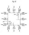
- FIG. 12 shows an alternative means for avoiding improper crossovers, this not requiring additional bits.
- a cell 320 has AND gates 332 and 334 with outputs providing AVAILSW (Rows) and AVAILNE (Cols) signals respectively.
- the gates 332 and 334 provides the signals by ANDing the AVAILS (Cols) or AVAILE (Rows) input signal with what in cell 250 would have been the AVAILSW (Rows) or AVAILNE (Cols) output signal respectively.
- modified AVAILSW (Rows) and AVAILNE (Cols) signals are produced by ANDing the corresponding unmodified (Col) or (Row) signal in either case with the respective (Row) or (Col) AVAIL input signal at 45 0 to it.
- cell 320 operates as follows. Referring to Figure 9(a) once more, cell 240a4 outputs a TRUE row availability signal to cell 240a3 at all times other than when a row connection exists between cells 240a, and 240a4. Accordingly, cell 240a3 uses its TRUE or FALSE row availability signal to modify its column availability output signal to cell 240a 2 . This is achieved by gate 334 in cell 240a3 ANDing the AVAILE (Rows) input signal with the internal equivalent of the cell 250 AVAILNE (Cols) output signal to provide a modified AVAILNE (Cols) output signal to cell 240a 2 . Priority to row connection is given in this case.
- cell 240b 4 outputs a TRUE column availability signal to cell 240b 2 at all times other than when a column connection exists between cells 240b 1 and 240b 4 .
- gate 332 in cell 240b 2 ANDs this column availability input signal with its internally generated AVAILSE (Rows) signal to produce a modified AVAILSE (Rows) output signal to cell 240b 3 .
- priority is given to column connection.
- the Figure 11 arrangement requires only two additional gates to inhibit improper crossover. It does however reduce percentage cell utilisation. This arises because faulty cells output FALSE availability signals in all directions. Neighbours of a cell cannot distinguish FALSE availability signals indicating faulty cells from those indicating the presence of an SE/NW connection. This means that a link cannot be formed between two cells respectively above and to the left of a faulty cell. The situation could of course be alleviated by providing an SE/NW bypass implementable in the event of cell failure under appropriate request and availability conditions.
Landscapes
- Engineering & Computer Science (AREA)
- Computer Hardware Design (AREA)
- Theoretical Computer Science (AREA)
- Computing Systems (AREA)
- Physics & Mathematics (AREA)
- General Engineering & Computer Science (AREA)
- General Physics & Mathematics (AREA)
- Hardware Redundancy (AREA)
- Data Exchanges In Wide-Area Networks (AREA)
Applications Claiming Priority (4)
| Application Number | Priority Date | Filing Date | Title |
|---|---|---|---|
| GB858502186A GB8502186D0 (en) | 1985-01-29 | 1985-01-29 | Processing cell |
| GB8502186 | 1985-01-29 | ||
| GB8515649 | 1985-06-20 | ||
| GB858515649A GB8515649D0 (en) | 1985-01-29 | 1985-06-20 | Processing cell |
Publications (3)
| Publication Number | Publication Date |
|---|---|
| EP0190813A2 true EP0190813A2 (de) | 1986-08-13 |
| EP0190813A3 EP0190813A3 (en) | 1988-05-11 |
| EP0190813B1 EP0190813B1 (de) | 1991-09-18 |
Family
ID=26288728
Family Applications (1)
| Application Number | Title | Priority Date | Filing Date |
|---|---|---|---|
| EP86300018A Expired EP0190813B1 (de) | 1985-01-29 | 1986-01-03 | Verarbeitungszelle für fehlertolerante Matrixanordnungen |
Country Status (3)
| Country | Link |
|---|---|
| US (1) | US5065308A (de) |
| EP (1) | EP0190813B1 (de) |
| DE (1) | DE3681463D1 (de) |
Cited By (2)
| Publication number | Priority date | Publication date | Assignee | Title |
|---|---|---|---|---|
| GB2243931A (en) * | 1990-05-11 | 1991-11-13 | Anamartic Ltd | Chaining circuit modules |
| US5513313A (en) * | 1993-01-19 | 1996-04-30 | International Business Machines Corporation | Method for generating hierarchical fault-tolerant mesh architectures |
Families Citing this family (65)
| Publication number | Priority date | Publication date | Assignee | Title |
|---|---|---|---|---|
| GB9027663D0 (en) * | 1990-12-20 | 1991-02-13 | Sandoz Ltd | Light-stabilizing compositions |
| US5825773A (en) * | 1991-03-20 | 1998-10-20 | Hitachi, Ltd. | Switching system for transferring broadcast packet held in broadcast buffer received from input port to output ports according to the state of each output port |
| JP3679813B2 (ja) * | 1991-07-22 | 2005-08-03 | 株式会社日立製作所 | 並列計算機 |
| US5271014A (en) * | 1992-05-04 | 1993-12-14 | International Business Machines Corporation | Method and apparatus for a fault-tolerant mesh with spare nodes |
| US5758053A (en) * | 1992-07-22 | 1998-05-26 | Hitachi, Ltd. | Fault handling and recovery for system having plural processors |
| US5717947A (en) * | 1993-03-31 | 1998-02-10 | Motorola, Inc. | Data processing system and method thereof |
| FR2711436B1 (fr) * | 1993-10-18 | 1996-01-05 | France Telecom | Procédé perfectionné de fonctionnement en parallèle de plusieurs unités de calcul, notamment en traitement d'images, et architecture correspondante. |
| US6408402B1 (en) | 1994-03-22 | 2002-06-18 | Hyperchip Inc. | Efficient direct replacement cell fault tolerant architecture |
| EP1046994A3 (de) * | 1994-03-22 | 2000-12-06 | Hyperchip Inc. | Direkte Zellenersetzung für fehlertolerante Architektur mit gänzlich integrierten Systemen und mit Mitteln zur direkten Kommunikation mit Systembediener |
| US7266725B2 (en) | 2001-09-03 | 2007-09-04 | Pact Xpp Technologies Ag | Method for debugging reconfigurable architectures |
| DE19651075A1 (de) | 1996-12-09 | 1998-06-10 | Pact Inf Tech Gmbh | Einheit zur Verarbeitung von numerischen und logischen Operationen, zum Einsatz in Prozessoren (CPU's), Mehrrechnersystemen, Datenflußprozessoren (DFP's), digitalen Signal Prozessoren (DSP's) oder dergleichen |
| DE19654593A1 (de) | 1996-12-20 | 1998-07-02 | Pact Inf Tech Gmbh | Umkonfigurierungs-Verfahren für programmierbare Bausteine zur Laufzeit |
| DE19654595A1 (de) | 1996-12-20 | 1998-07-02 | Pact Inf Tech Gmbh | I0- und Speicherbussystem für DFPs sowie Bausteinen mit zwei- oder mehrdimensionaler programmierbaren Zellstrukturen |
| ATE243390T1 (de) | 1996-12-27 | 2003-07-15 | Pact Inf Tech Gmbh | Verfahren zum selbständigen dynamischen umladen von datenflussprozessoren (dfps) sowie bausteinen mit zwei- oder mehrdimensionalen programmierbaren zellstrukturen (fpgas, dpgas, o.dgl.) |
| DE19654846A1 (de) | 1996-12-27 | 1998-07-09 | Pact Inf Tech Gmbh | Verfahren zum selbständigen dynamischen Umladen von Datenflußprozessoren (DFPs) sowie Bausteinen mit zwei- oder mehrdimensionalen programmierbaren Zellstrukturen (FPGAs, DPGAs, o. dgl.) |
| US6542998B1 (en) | 1997-02-08 | 2003-04-01 | Pact Gmbh | Method of self-synchronization of configurable elements of a programmable module |
| DE19704728A1 (de) | 1997-02-08 | 1998-08-13 | Pact Inf Tech Gmbh | Verfahren zur Selbstsynchronisation von konfigurierbaren Elementen eines programmierbaren Bausteines |
| DE19704742A1 (de) * | 1997-02-11 | 1998-09-24 | Pact Inf Tech Gmbh | Internes Bussystem für DFPs, sowie Bausteinen mit zwei- oder mehrdimensionalen programmierbaren Zellstrukturen, zur Bewältigung großer Datenmengen mit hohem Vernetzungsaufwand |
| US8686549B2 (en) | 2001-09-03 | 2014-04-01 | Martin Vorbach | Reconfigurable elements |
| DE19861088A1 (de) | 1997-12-22 | 2000-02-10 | Pact Inf Tech Gmbh | Verfahren zur Reparatur von integrierten Schaltkreisen |
| US7003660B2 (en) | 2000-06-13 | 2006-02-21 | Pact Xpp Technologies Ag | Pipeline configuration unit protocols and communication |
| DE10081643D2 (de) | 1999-06-10 | 2002-05-29 | Pact Inf Tech Gmbh | Sequenz-Partitionierung auf Zellstrukturen |
| FR2795840B1 (fr) * | 1999-07-02 | 2001-08-31 | Commissariat Energie Atomique | Reseau de processeurs paralleles avec tolerance aux fautes de ces processeurs, et procede de reconfiguration applicable a un tel reseau |
| FR2795839B1 (fr) * | 1999-07-02 | 2001-09-07 | Commissariat Energie Atomique | Procede de reconfiguration applicable a un reseau d'elements fonctionnels identiques |
| US7002975B2 (en) * | 2000-08-11 | 2006-02-21 | Texas Instruments Incorporated | Multiprocessor network node failure detection and recovery |
| US8058899B2 (en) | 2000-10-06 | 2011-11-15 | Martin Vorbach | Logic cell array and bus system |
| AU2002220600A1 (en) | 2000-10-06 | 2002-04-15 | Pact Informationstechnologie Gmbh | Cell system with segmented intermediate cell structure |
| GB2370380B (en) | 2000-12-19 | 2003-12-31 | Picochip Designs Ltd | Processor architecture |
| US6990555B2 (en) | 2001-01-09 | 2006-01-24 | Pact Xpp Technologies Ag | Method of hierarchical caching of configuration data having dataflow processors and modules having two- or multidimensional programmable cell structure (FPGAs, DPGAs, etc.) |
| US7444531B2 (en) | 2001-03-05 | 2008-10-28 | Pact Xpp Technologies Ag | Methods and devices for treating and processing data |
| US9037807B2 (en) | 2001-03-05 | 2015-05-19 | Pact Xpp Technologies Ag | Processor arrangement on a chip including data processing, memory, and interface elements |
| US7844796B2 (en) | 2001-03-05 | 2010-11-30 | Martin Vorbach | Data processing device and method |
| US7581076B2 (en) | 2001-03-05 | 2009-08-25 | Pact Xpp Technologies Ag | Methods and devices for treating and/or processing data |
| US7210129B2 (en) | 2001-08-16 | 2007-04-24 | Pact Xpp Technologies Ag | Method for translating programs for reconfigurable architectures |
| WO2002103532A2 (de) | 2001-06-20 | 2002-12-27 | Pact Xpp Technologies Ag | Verfahren zur bearbeitung von daten |
| US7996827B2 (en) | 2001-08-16 | 2011-08-09 | Martin Vorbach | Method for the translation of programs for reconfigurable architectures |
| US7434191B2 (en) | 2001-09-03 | 2008-10-07 | Pact Xpp Technologies Ag | Router |
| US8686475B2 (en) | 2001-09-19 | 2014-04-01 | Pact Xpp Technologies Ag | Reconfigurable elements |
| AU2002338729A1 (en) * | 2001-09-19 | 2003-04-01 | Pact Xpp Technologies Ag | Router |
| US7577822B2 (en) | 2001-12-14 | 2009-08-18 | Pact Xpp Technologies Ag | Parallel task operation in processor and reconfigurable coprocessor configured based on information in link list including termination information for synchronization |
| AU2003208266A1 (en) | 2002-01-19 | 2003-07-30 | Pact Xpp Technologies Ag | Reconfigurable processor |
| WO2003071432A2 (de) | 2002-02-18 | 2003-08-28 | Pact Xpp Technologies Ag | Bussysteme und rekonfigurationsverfahren |
| US8914590B2 (en) | 2002-08-07 | 2014-12-16 | Pact Xpp Technologies Ag | Data processing method and device |
| GB2417586B (en) * | 2002-07-19 | 2007-03-28 | Picochip Designs Ltd | Processor array |
| AU2003286131A1 (en) | 2002-08-07 | 2004-03-19 | Pact Xpp Technologies Ag | Method and device for processing data |
| US7657861B2 (en) | 2002-08-07 | 2010-02-02 | Pact Xpp Technologies Ag | Method and device for processing data |
| WO2004038599A1 (de) | 2002-09-06 | 2004-05-06 | Pact Xpp Technologies Ag | Rekonfigurierbare sequenzerstruktur |
| EP1634182A2 (de) * | 2003-06-17 | 2006-03-15 | PACT XPP Technologies AG | Datenverarbeitungseinrichtung und verfahren |
| JP4700611B2 (ja) | 2003-08-28 | 2011-06-15 | ペーアーツェーテー イクスペーペー テクノロジーズ アクチエンゲゼルシャフト | データ処理装置およびデータ処理方法 |
| US20070174655A1 (en) * | 2006-01-18 | 2007-07-26 | Brown Kyle G | System and method of implementing automatic resource outage handling |
| WO2007082730A1 (de) | 2006-01-18 | 2007-07-26 | Pact Xpp Technologies Ag | Hardwaredefinitionsverfahren |
| US8078907B2 (en) * | 2006-01-19 | 2011-12-13 | Silicon Graphics, Inc. | Failsoft system for multiple CPU system |
| GB2454865B (en) | 2007-11-05 | 2012-06-13 | Picochip Designs Ltd | Power control |
| US20100272811A1 (en) * | 2008-07-23 | 2010-10-28 | Alkermes,Inc. | Complex of trospium and pharmaceutical compositions thereof |
| US20100241783A1 (en) * | 2009-03-23 | 2010-09-23 | Honeywell International Inc. | Memory node for use within a data storage system having a plurality of interconnected memory nodes |
| GB2470037B (en) | 2009-05-07 | 2013-07-10 | Picochip Designs Ltd | Methods and devices for reducing interference in an uplink |
| GB2470771B (en) | 2009-06-05 | 2012-07-18 | Picochip Designs Ltd | A method and device in a communication network |
| GB2470891B (en) | 2009-06-05 | 2013-11-27 | Picochip Designs Ltd | A method and device in a communication network |
| GB2474071B (en) | 2009-10-05 | 2013-08-07 | Picochip Designs Ltd | Femtocell base station |
| GB2482869B (en) | 2010-08-16 | 2013-11-06 | Picochip Designs Ltd | Femtocell access control |
| GB2489716B (en) | 2011-04-05 | 2015-06-24 | Intel Corp | Multimode base system |
| GB2489919B (en) | 2011-04-05 | 2018-02-14 | Intel Corp | Filter |
| GB2491098B (en) | 2011-05-16 | 2015-05-20 | Intel Corp | Accessing a base station |
| US8990616B2 (en) * | 2012-09-28 | 2015-03-24 | International Business Machines Corporation | Final faulty core recovery mechanisms for a two-dimensional network on a processor array |
| US9160617B2 (en) * | 2012-09-28 | 2015-10-13 | International Business Machines Corporation | Faulty core recovery mechanisms for a three-dimensional network on a processor array |
Family Cites Families (9)
| Publication number | Priority date | Publication date | Assignee | Title |
|---|---|---|---|---|
| US3970993A (en) * | 1974-01-02 | 1976-07-20 | Hughes Aircraft Company | Cooperative-word linear array parallel processor |
| US4247892A (en) * | 1978-10-12 | 1981-01-27 | Lawrence Patrick N | Arrays of machines such as computers |
| US4304002A (en) * | 1978-11-23 | 1981-12-01 | International Computers Limited | Data processing system with error checking |
| GB2074351B (en) * | 1980-03-28 | 1984-01-04 | Int Computers Ltd | Data processing system |
| ZA811458B (en) * | 1980-03-28 | 1982-03-31 | Int Computers Ltd | Data processing system |
| US4593351A (en) * | 1981-06-12 | 1986-06-03 | International Business Machines Corporation | High speed machine for the physical design of very large scale integrated circuits |
| GB2114782B (en) * | 1981-12-02 | 1985-06-05 | Burroughs Corp | Branched-spiral wafer-scale integrated circuit |
| CA1219965A (en) * | 1983-04-11 | 1987-03-31 | Allen P. Clarke | Self repair large scale integrated circuit |
| US4591980A (en) * | 1984-02-16 | 1986-05-27 | Xerox Corporation | Adaptive self-repairing processor array |
-
1986
- 1986-01-03 DE DE8686300018T patent/DE3681463D1/de not_active Expired - Lifetime
- 1986-01-03 EP EP86300018A patent/EP0190813B1/de not_active Expired
-
1991
- 1991-02-22 US US07/659,538 patent/US5065308A/en not_active Expired - Lifetime
Non-Patent Citations (1)
| Title |
|---|
| AFIPS CONFERENCE PROCEEDINGS, 1983 NATIONAL COMPUTER CONFERENCE, Anaheim, California, 16th-19th May 1983, pages 565-577, AFIPS Press, Arlington, US; M. SAMI et al.: "Reconfigurable architectures for VLSI processing arrays" * |
Cited By (2)
| Publication number | Priority date | Publication date | Assignee | Title |
|---|---|---|---|---|
| GB2243931A (en) * | 1990-05-11 | 1991-11-13 | Anamartic Ltd | Chaining circuit modules |
| US5513313A (en) * | 1993-01-19 | 1996-04-30 | International Business Machines Corporation | Method for generating hierarchical fault-tolerant mesh architectures |
Also Published As
| Publication number | Publication date |
|---|---|
| US5065308A (en) | 1991-11-12 |
| EP0190813B1 (de) | 1991-09-18 |
| DE3681463D1 (de) | 1991-10-24 |
| EP0190813A3 (en) | 1988-05-11 |
Similar Documents
| Publication | Publication Date | Title |
|---|---|---|
| EP0190813B1 (de) | Verarbeitungszelle für fehlertolerante Matrixanordnungen | |
| EP0398552B1 (de) | Ultrahöchstintegrierte Schaltungsbauweise mit linearen Verbindungen | |
| US4970724A (en) | Redundancy and testing techniques for IC wafers | |
| EP0256661A2 (de) | Feldrechner | |
| US5530813A (en) | Field-programmable electronic crossbar system and method for using same | |
| US5371422A (en) | Programmable logic device having multiplexers and demultiplexers randomly connected to global conductors for interconnections between logic elements | |
| EP1080531B1 (de) | Spezielle schnittstellenarchitektur für eine hybride schaltung | |
| US5208491A (en) | Field programmable gate array | |
| JP3414770B2 (ja) | マルチプレクサ相互接続を用いた高密度な消去可能型プログラマブル論理デバイスのアーキテクチャ | |
| US5491353A (en) | Configurable cellular array | |
| US5455525A (en) | Hierarchically-structured programmable logic array and system for interconnecting logic elements in the logic array | |
| US6681316B1 (en) | Network of parallel processors to faults-tolerant towards said processors and reconfiguration method applicable to such a network | |
| JPH0766718A (ja) | プログラム可能論理用ウェファ・スケール構造 | |
| US5394033A (en) | Structure and method for implementing hierarchical routing pools in a programmable logic circuit | |
| US4415973A (en) | Array processor with stand-by for replacing failed section | |
| GB2287114A (en) | Flexible programmable logic device interconnections | |
| JPH0379126A (ja) | 構成可能論理素子 | |
| US7360005B2 (en) | Software programmable multiple function integrated circuit module | |
| JPH10233676A (ja) | 論理アレイブロック内でローカル相互接続ラインを配列する方法およびプログラマブル論理回路 | |
| US6094066A (en) | Tiered routing architecture for field programmable gate arrays | |
| US6996736B1 (en) | Programmable clock network for distributing clock signals to and between first and second sections of an integrated circuit | |
| CN117370268A (zh) | 具有多类型的可编程阵列和灵活时钟选择的可编程逻辑块 | |
| WO2000044046A1 (fr) | Circuit integre et son procede de conception | |
| US5404055A (en) | Input routing pool | |
| JP2643585B2 (ja) | 集積回路 |
Legal Events
| Date | Code | Title | Description |
|---|---|---|---|
| PUAI | Public reference made under article 153(3) epc to a published international application that has entered the european phase |
Free format text: ORIGINAL CODE: 0009012 |
|
| AK | Designated contracting states |
Kind code of ref document: A2 Designated state(s): DE FR GB IT NL |
|
| PUAL | Search report despatched |
Free format text: ORIGINAL CODE: 0009013 |
|
| AK | Designated contracting states |
Kind code of ref document: A3 Designated state(s): DE FR GB IT NL |
|
| 17P | Request for examination filed |
Effective date: 19880720 |
|
| 17Q | First examination report despatched |
Effective date: 19900322 |
|
| 17Q | First examination report despatched |
Effective date: 19900521 |
|
| GRAA | (expected) grant |
Free format text: ORIGINAL CODE: 0009210 |
|
| AK | Designated contracting states |
Kind code of ref document: B1 Designated state(s): DE FR GB IT NL |
|
| ITF | It: translation for a ep patent filed | ||
| REF | Corresponds to: |
Ref document number: 3681463 Country of ref document: DE Date of ref document: 19911024 |
|
| ET | Fr: translation filed | ||
| PLBE | No opposition filed within time limit |
Free format text: ORIGINAL CODE: 0009261 |
|
| STAA | Information on the status of an ep patent application or granted ep patent |
Free format text: STATUS: NO OPPOSITION FILED WITHIN TIME LIMIT |
|
| 26N | No opposition filed | ||
| PGFP | Annual fee paid to national office [announced via postgrant information from national office to epo] |
Ref country code: FR Payment date: 20011210 Year of fee payment: 17 |
|
| REG | Reference to a national code |
Ref country code: GB Ref legal event code: 732E |
|
| PGFP | Annual fee paid to national office [announced via postgrant information from national office to epo] |
Ref country code: DE Payment date: 20011219 Year of fee payment: 17 |
|
| REG | Reference to a national code |
Ref country code: GB Ref legal event code: IF02 |
|
| REG | Reference to a national code |
Ref country code: FR Ref legal event code: TP |
|
| NLS | Nl: assignments of ep-patents |
Owner name: QINETIQ LIMITED |
|
| PGFP | Annual fee paid to national office [announced via postgrant information from national office to epo] |
Ref country code: NL Payment date: 20021212 Year of fee payment: 18 Ref country code: GB Payment date: 20021212 Year of fee payment: 18 |
|
| PG25 | Lapsed in a contracting state [announced via postgrant information from national office to epo] |
Ref country code: DE Free format text: LAPSE BECAUSE OF NON-PAYMENT OF DUE FEES Effective date: 20030801 |
|
| PG25 | Lapsed in a contracting state [announced via postgrant information from national office to epo] |
Ref country code: FR Free format text: LAPSE BECAUSE OF NON-PAYMENT OF DUE FEES Effective date: 20030930 |
|
| REG | Reference to a national code |
Ref country code: FR Ref legal event code: ST |
|
| PG25 | Lapsed in a contracting state [announced via postgrant information from national office to epo] |
Ref country code: GB Free format text: LAPSE BECAUSE OF NON-PAYMENT OF DUE FEES Effective date: 20040103 |
|
| PG25 | Lapsed in a contracting state [announced via postgrant information from national office to epo] |
Ref country code: NL Free format text: LAPSE BECAUSE OF NON-PAYMENT OF DUE FEES Effective date: 20040801 |
|
| GBPC | Gb: european patent ceased through non-payment of renewal fee |
Effective date: 20040103 |
|
| NLV4 | Nl: lapsed or anulled due to non-payment of the annual fee |
Effective date: 20040801 |
|
| PG25 | Lapsed in a contracting state [announced via postgrant information from national office to epo] |
Ref country code: IT Free format text: LAPSE BECAUSE OF NON-PAYMENT OF DUE FEES Effective date: 20050103 |