EP0191440A1 - Appareil de lithographie pour la réalisation de microstructures - Google Patents
Appareil de lithographie pour la réalisation de microstructures Download PDFInfo
- Publication number
- EP0191440A1 EP0191440A1 EP86101630A EP86101630A EP0191440A1 EP 0191440 A1 EP0191440 A1 EP 0191440A1 EP 86101630 A EP86101630 A EP 86101630A EP 86101630 A EP86101630 A EP 86101630A EP 0191440 A1 EP0191440 A1 EP 0191440A1
- Authority
- EP
- European Patent Office
- Prior art keywords
- lithography device
- line
- aperture diaphragm
- hole structure
- recesses
- Prior art date
- Legal status (The legal status is an assumption and is not a legal conclusion. Google has not performed a legal analysis and makes no representation as to the accuracy of the status listed.)
- Granted
Links
Images



Classifications
-
- H—ELECTRICITY
- H01—ELECTRIC ELEMENTS
- H01J—ELECTRIC DISCHARGE TUBES OR DISCHARGE LAMPS
- H01J37/00—Discharge tubes with provision for introducing objects or material to be exposed to the discharge, e.g. for the purpose of examination or processing thereof
- H01J37/30—Electron-beam or ion-beam tubes for localised treatment of objects
- H01J37/317—Electron-beam or ion-beam tubes for localised treatment of objects for changing properties of the objects or for applying thin layers thereon, e.g. for ion implantation
- H01J37/3174—Particle-beam lithography, e.g. electron beam lithography
- H01J37/3177—Multi-beam, e.g. fly's eye, comb probe
-
- B—PERFORMING OPERATIONS; TRANSPORTING
- B82—NANOTECHNOLOGY
- B82Y—SPECIFIC USES OR APPLICATIONS OF NANOSTRUCTURES; MEASUREMENT OR ANALYSIS OF NANOSTRUCTURES; MANUFACTURE OR TREATMENT OF NANOSTRUCTURES
- B82Y10/00—Nanotechnology for information processing, storage or transmission, e.g. quantum computing or single electron logic
-
- B—PERFORMING OPERATIONS; TRANSPORTING
- B82—NANOTECHNOLOGY
- B82Y—SPECIFIC USES OR APPLICATIONS OF NANOSTRUCTURES; MEASUREMENT OR ANALYSIS OF NANOSTRUCTURES; MANUFACTURE OR TREATMENT OF NANOSTRUCTURES
- B82Y40/00—Manufacture or treatment of nanostructures
-
- H—ELECTRICITY
- H01—ELECTRIC ELEMENTS
- H01J—ELECTRIC DISCHARGE TUBES OR DISCHARGE LAMPS
- H01J37/00—Discharge tubes with provision for introducing objects or material to be exposed to the discharge, e.g. for the purpose of examination or processing thereof
- H01J37/30—Electron-beam or ion-beam tubes for localised treatment of objects
- H01J37/3002—Details
- H01J37/3007—Electron or ion-optical systems
Definitions
- the invention relates to a lithography device for producing microstructures, in particular for semiconductors, according to the preamble of patent claim 1.
- Such a device is from the IEEE Transactions on Electron Devices, Vol. ED-26, No. 4, April 1979, pp. 663-674, in particular FIGS. 3 and 4.
- a higher throughput of exposed semiconductor structures can be expected than in the case of a lithography device with only one probe which sweeps over a surface to be structured in a grid pattern.
- the production of semiconductor structures using a lithography device is e.g. in the Siemens Research and Development Reports, Vol. 9 - (1980) No. 3, pp. 174-178. In this regard, reference is made in particular to FIG. 8 and the associated text on page 178.
- each individual corpuscular beam probe can be deflected by applying a blanking voltage to a deflection capacitor, the electrodes of which are arranged on the edge side of the relevant probe-producing recess of the aperture diaphragm, so that it hits the blanking diaphragm and is thus blanked out of the further beam path becomes.
- the probe-producing recesses the dimensions of which are very small compared to the dimensions of the circular area illuminated by the corpuscular beam source on the aperture diaphragm, permit only relatively small probe currents.
- each reduction in the probe current leads to an increase in the exposure times for the points of the resist to be exposed, which are swept by the corpuscular beam probes, so that the expected higher throughput (compared to that of a lithography device with a single grid-shaped deflected probe) is only partially achieved.
- the invention has for its object to provide a lithography device of the type mentioned that enables a significantly higher throughput of exposed microstructures than the known lithography device mentioned above. This is achieved according to the invention by designing the lithography device according to the characterizing part of patent claim 1.
- the advantage that can be achieved with the invention is, in particular, that the corpuscular beam probes, despite the small dimensions of the probe-producing recesses, carry a relatively high probe current and therefore permit a high exposure speed for the individual points of the resist.
- Claims 2 to 16 are directed to advantageous refinements and developments of the lithography device according to the invention.
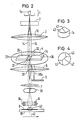
- the lithography device shown schematically in FIGS. 1 and 2 comprises an electron beam source 1, a cylindrical lens 2, a condenser lens 3, a controllable aperture diaphragm 4, a blanking diaphragm 5, an imaging optic consisting of lenses 6, 7 and an objective lens OL and a deflection system 8, below which is a body 9 to be structured, in particular semiconductor body.
- This is attached to a table 1 0, which is advantageously mounted rotatably about a vertical axis 11.
- the electron beams emerging from a cathode 1 are combined by the cylindrical lens 2 and the condenser lens 3 to form a band beam which is delimited by the peripheral beams 12 and 13 in the view according to FIG. 1. Perpendicular to it, i.e. 2, it has the edge rays 14 and 15. As can be seen from this, the cross section of the band beam parallel to the image plane of FIG. 1 is dimensioned much larger than parallel to the image plane of FIG. 2. Between the cylindrical lens 2 and the condenser lens 3, a slit diaphragm 16 is expediently provided, which limits the band beam to Edge rays 14 and 15 causes.
- the disk-shaped aperture diaphragm 4 is provided with a line-shaped multi-hole structure.
- rectangular or square recesses 17 to 22 are provided for this purpose, each starting from a central, dashed line 23 and being alternately offset to one side and the other.
- Another electrode 30 extends along line 23 and represents a common counter electrode for all recesses. It is connected to a connection 31.
- the multi-hole structure consists of a series of rectangular or square recesses 32 which lie along the line 23 without being offset from one another.
- the multi-hole structure consists of a series of rectangular or square recesses 32 which lie along the line 23 without being offset from one another.
- only one recess 32 is shown greatly enlarged, the other recesses being indicated by dashed lines 33.
- electrodes 3 4 and 35 are arranged at the edges of the recesses 32, which are connected to connections 36 and 37.
- the band jet is aligned so that its largest cross-sectional dimension, which is given by the marginal rays 12 and 13, lies in the direction of line 23, while its smallest dimension is perpendicular thereto and the width of the multi-hole structure, taking into account any mutual offset of the recesses (Fig. 1 ) corresponds or only slightly exceeds this This ensures; that only the immediate area of the multi-hole structure is illuminated by the band beam, so that a large part of the energy emitted by the electron beam source 1 is available for the shaping of the electron beam probes.
- Each of these probes consists of one through one of the recesses 17 to 22 or 32 part of the band beam passing through. 2, the electron beam probe formed by the recess 32 is designated 38.
- a voltage is switched to the connections 36 and 37, through which the electrode 34 is placed at a more positive potential than the electrode 35, the probe 38 is deflected into the position 38a and thereby caught by the blanking orifice 5, so that it comes out of the further beam path is hidden.
- Each undeflected probe, for example 38, is available for exposing the surface of the body 9 or a resist applied thereon. 1, a positive voltage is supplied to the electrode 24 while the electrode 31 is at reference potential. If a probe formed by the recess 18 is to be faded out, a negative voltage is applied to the electrode 26 If 5 is designed as a slit diaphragm, a positive voltage is also permissible at 26.
- the probe cross sections which are in the plane of the aperture diaphragm 4 by the dimensions of the recesses, e.g. 17, are shown reduced in size by means of the lenses 6 and 7 in a plane 39, which corresponds to a reduction of the line 23 to a line 23 '.
- the objective lens OL then images the cross sections of the electron beam probes on the surface of the body 9, which is indicated by 40.
- the structure generation on the body 9 takes place according to Fig. 1 so that the entirety of all not blanked electron beam probes after exposure of the points of the body 9 hit or a resist covering them, for example by means of the deflection system 8 in an approximately perpendicular to the projection of the line 23 Direction is moved relative to the body 9, namely by a probe dimension.
- the neighboring probe line thus sought is then exposed in an analog manner.
- any exposure pattern can be generated on the surface of FIG. 9, the smallest structural detail of which corresponds to the cross-sectional dimension of a probe, measured on the surface of FIG. 9. 2 accordingly applies that the entirety of the probes which have not been blanked out after an exposure process are each shifted by a projected probe dimension relative to the body 9, which is indicated by the arrow 41.
- FIGS. 1 and 2 illustrate the mapping of the recesses 17, etc. of the aperture diaphragm 4 onto the surface of the body 9.
- Fig. 3 shows a preferred embodiment of the cathode 1 a, in the form of a single-crystal stud cathode made of lanthanum hexaboride (LaB.), Which ends in a cutting edge 42.
- This shape is obtained, for example, by first grinding a cylindrical pin cathode from two sides, so that a cutting edge 42 is formed, the length of which corresponds to the diameter of the pin, and then grinding two further surfaces 43, which are then the length between them of the cutting edge 42.
- the cutting edge 42 and the surfaces 43 are clearly recognizable.
- the ground surfaces preferably correspond to 100 planes of the crystal, or other planes that represent surfaces with a low work function.
- a high-resistance substrate film for example made of silicon, is provided with the recesses 17 to 22 already described.
- the electrodes 24, 25, 26, etc., which are used for probe blanking, are designed as conductor tracks which are widened at the end and which consist, for example, of gold.
- the common electrode 30 is preferably also made of gold and runs in a meandering shape between the recesses, wherein it is provided with sufficiently wide intermediate webs 45 in order to achieve good contact between its individual parts.
- the surface of FIG. 4 facing the electron beam source 1 is provided outside the hole structures with a conductive covering, via which the impinging electrons are derived.
- the aperture diaphragm 4 can be supplemented by a further aperture diaphragm 4a according to FIG. 6.
- This also consists of a high-resistance substrate film and has recesses 17a to 21a which coincide with the recesses 17 to 21 when the diaphragms are precisely adjusted to one another.
- Two electrodes 17b, 17c to 22b, 22c are provided on the edge side of the recesses 17a to 22a, which are connected to connections. Voltages can be applied to these, which deflect the electron beam probes parallel to the longitudinal direction of the line-shaped multi-hole structure in order to correct optical errors (e.g. opening errors of the condenser lenses, distortion of the imaging optics, etc.).
- the electrode structures of FIG. 4a are also advantageously designed as conductor tracks and consist e.g. of gold.
- the aperture diaphragms 4, 4a can be produced using planar technology with conventional lithography methods.
- the aperture diaphragms 4 and 4a formed in the manner described can be designed with particular advantage for a large number of recesses 17 etc. For example, 2048 recesses are conceivable with which a corresponding number of electron beam probes are generated. If one assumes a square shape of the recesses 17 etc. with a side length of 10 ⁇ m and reduces the probe size by a factor of 100 with the aid of the imaging optics, individual image points with a side length of 0.1 ⁇ m result.
- the length of the multiple-hole structure on the aperture diaphragm 4 is approximately 20.5 mm, with such a device it is possible, for example, to produce structures in the 0.1 UM range, such as those used for integrated circuits based on GaAs or for components in optical communications technology, for example Lattice structures for solid-state lasers are required.
- Different aperture diaphragms can be provided for different grid dimensions of the structures to be produced, the recesses of which are appropriately dimensioned and arranged.
- Fig. 7 only the parts of the device lying below the aperture diaphragm 4 are shown. Above 4 there are the same parts as in the arrangement according to FIG. 1.
- the illumination beam path is designated by 46 while 47 represents the light path for imaging of the recess 7 1 on the surface of. 9
- the imaging scale is changed by means of a zoom lens 48, which takes the place of the lens 6 from FIG. 1. Such a lens is already mentioned on page 177 of the Siemens research and development reports mentioned above (in particular FIG. 6 and the associated text).
- main winding 49 which is supplemented by three additional windings 50 which are symmetrical to their longitudinal axis and effect a focal length adjustment. If the additional windings are fed in such a way that the middle one of them weakens the main field generated by 49, while the lower and the upper additional winding 50 reinforce this main field, there is a deformation of the main field which corresponds to a larger focal length of 48. If these influences are reversed, the focal length is reduced. The effective lens excitation remains unaffected.
- Two further windings 51 also arranged symmetrically to the longitudinal axis of the lens 48, bring about additional changes in the lens field, which are equivalent to a longitudinal displacement of the lens parts 4 9 and 50 in the direction of the aperture diaphragm 4 or in the opposite direction. If the main field of 48 is weakened by the upper winding 51 and reinforced by the lower winding 51, there is the effect of a longitudinal displacement of 48 downwards, with a reversal of these influences on the main field, such an upward movement.
- the focal length is now reduced by 48 and the main lens field is shifted towards the aperture diaphragm 4 by an amount corresponding to this reduction, the reduction in the recesses 17 projected onto 9, etc., caused by the lenses 48 and 7 decreases, at the same time the probe cross-section effective for the exposure increases, so that there is an increase in the grid dimension of the structure to be produced.
- a reversal of the influences on the main field of 48 then leads to a reduction in the structural grid size.
- the lenses 48 and 7 advantageously have a telecentric beam path and opposite excitations, which is indicated by the arrows 52. This practically avoids distortion color errors, magnification color errors and isotropic distortions of the lens system 48, 7.
- the 7 is supplemented by two lenses 53 and 54, between which the deflection system 55 is located.
- the lenses 53 and 54 are also preferably designed with a telecentric beam path and opposite excitation in order to eliminate the errors mentioned. Such a design of lens pairs can be found in DE-PS 25 15 549. The Boersch effect is also minimized by using the band beam.
- the relative movement between the entirety of the electron beam probes and the body 9 can also be achieved by moving the table 10.
- a continuous rotary movement, for example, about axis 11 is also suitable for this purpose.
- An irradiation rate of approximately 1 cm 2 / s calculated according to the above example can thus be taken into account in a simple manner.
- the aperture diaphragm 4 according to FIG. 2 has a series of recesses 32 which are not offset with respect to one another and whose mutual distances correspond to the side length of a recess, after each individual exposure operation within the same line setting of the electron beam probes the latter has to be shifted by this side length in Direction of line 23 take place so that a complete exposure of the body 9 is ensured.
- This displacement is advantageously carried out by means of the deflection system 8 or 55.
- the idea of the invention includes not only the described embodiments in which electron beam probes are used, but also other corpuscular beam lithography devices, e.g. work with ion beam probes.
Landscapes
- Chemical & Material Sciences (AREA)
- Engineering & Computer Science (AREA)
- Nanotechnology (AREA)
- Analytical Chemistry (AREA)
- Physics & Mathematics (AREA)
- Crystallography & Structural Chemistry (AREA)
- Condensed Matter Physics & Semiconductors (AREA)
- General Physics & Mathematics (AREA)
- Manufacturing & Machinery (AREA)
- Mathematical Physics (AREA)
- Theoretical Computer Science (AREA)
- Electron Beam Exposure (AREA)
Applications Claiming Priority (2)
| Application Number | Priority Date | Filing Date | Title |
|---|---|---|---|
| DE3504714 | 1985-02-12 | ||
| DE19853504714 DE3504714A1 (de) | 1985-02-12 | 1985-02-12 | Lithografiegeraet zur erzeugung von mikrostrukturen |
Publications (2)
| Publication Number | Publication Date |
|---|---|
| EP0191440A1 true EP0191440A1 (fr) | 1986-08-20 |
| EP0191440B1 EP0191440B1 (fr) | 1989-05-24 |
Family
ID=6262280
Family Applications (1)
| Application Number | Title | Priority Date | Filing Date |
|---|---|---|---|
| EP86101630A Expired EP0191440B1 (fr) | 1985-02-12 | 1986-02-07 | Appareil de lithographie pour la réalisation de microstructures |
Country Status (4)
| Country | Link |
|---|---|
| US (1) | US4724328A (fr) |
| EP (1) | EP0191440B1 (fr) |
| JP (1) | JPS61187334A (fr) |
| DE (2) | DE3504714A1 (fr) |
Cited By (4)
| Publication number | Priority date | Publication date | Assignee | Title |
|---|---|---|---|---|
| EP0314216A1 (fr) * | 1987-10-29 | 1989-05-03 | Koninklijke Philips Electronics N.V. | Appareil à faisceau de particules chargées |
| EP0335711A3 (en) * | 1988-03-30 | 1990-07-18 | Fujitsu Limited | Charged particle beam exposure system |
| EP0360035A3 (fr) * | 1988-09-20 | 1990-08-22 | Siemens Aktiengesellschaft | Source de faisceau électrique |
| EP0379865A3 (fr) * | 1989-01-25 | 1991-06-05 | ICT Integrated Circuit Testing Gesellschaft für HalbleiterprÀ¼ftechnik mbH | Procédé d'examen d'un échantillon dans un appareil à faisceau corpusculaire |
Families Citing this family (45)
| Publication number | Priority date | Publication date | Assignee | Title |
|---|---|---|---|---|
| DE8634545U1 (de) * | 1986-12-23 | 1987-05-21 | Siemens AG, 1000 Berlin und 8000 München | Korpuskularstrahlgerät zur fehlerarmen Abbildung linienförmiger Objekte |
| EP0289885A1 (fr) * | 1987-05-08 | 1988-11-09 | Siemens Aktiengesellschaft | Système de diaphragme pour la production de plusieurs sondes de particules à section variable |
| US4902898A (en) * | 1988-04-26 | 1990-02-20 | Microelectronics Center Of North Carolina | Wand optics column and associated array wand and charged particle source |
| US5354695A (en) * | 1992-04-08 | 1994-10-11 | Leedy Glenn J | Membrane dielectric isolation IC fabrication |
| EP0344513A3 (fr) * | 1988-05-31 | 1991-01-16 | Siemens Aktiengesellschaft | Procédé de fabrication d'une plaque de commande pour un appareil de lithographie |
| EP0344515A3 (fr) * | 1988-05-31 | 1991-01-30 | Siemens Aktiengesellschaft | Procédé de fabrication d'un diaphragme de mise en forme du faisceau pour un appareil de lithographie |
| US4996441A (en) * | 1988-09-16 | 1991-02-26 | Siemens Aktiengesellschaft | Lithographic apparatus for structuring a subject |
| US4914305A (en) * | 1989-01-04 | 1990-04-03 | Eaton Corporation | Uniform cross section ion beam system |
| US5023458A (en) * | 1989-01-04 | 1991-06-11 | Eaton Corporation | Ion beam control system |
| EP0404608B1 (fr) * | 1989-05-19 | 1995-02-22 | Fujitsu Limited | Matrice de diaphragmes d'extinction de faisceau, son procédé de fabrication, appareil et procédé d'exposition par faisceau de particules chargées |
| US5262341A (en) * | 1989-05-19 | 1993-11-16 | Fujitsu Limited | Blanking aperture array and charged particle beam exposure method |
| US5126287A (en) * | 1990-06-07 | 1992-06-30 | Mcnc | Self-aligned electron emitter fabrication method and devices formed thereby |
| KR950002578B1 (ko) * | 1991-03-13 | 1995-03-23 | 후지쓰 가부시끼가이샤 | 전자빔 노광방법 |
| US6714625B1 (en) * | 1992-04-08 | 2004-03-30 | Elm Technology Corporation | Lithography device for semiconductor circuit pattern generation |
| US5369282A (en) * | 1992-08-03 | 1994-11-29 | Fujitsu Limited | Electron beam exposure method and system for exposing a pattern on a substrate with an improved accuracy and throughput |
| US5903098A (en) * | 1993-03-11 | 1999-05-11 | Fed Corporation | Field emission display device having multiplicity of through conductive vias and a backside connector |
| JPH08507643A (ja) * | 1993-03-11 | 1996-08-13 | フェド.コーポレイション | エミッタ先端構造体及び該エミッタ先端構造体を備える電界放出装置並びにその製造方法 |
| US5534743A (en) * | 1993-03-11 | 1996-07-09 | Fed Corporation | Field emission display devices, and field emission electron beam source and isolation structure components therefor |
| US5561339A (en) * | 1993-03-11 | 1996-10-01 | Fed Corporation | Field emission array magnetic sensor devices |
| US5309890A (en) * | 1993-07-30 | 1994-05-10 | Carrier Corporation | Dual-sided condensate trap for furnace |
| US5379749A (en) * | 1993-08-16 | 1995-01-10 | Carrier Corporation | Condensate trap for multi-poise furnace |
| US5583393A (en) * | 1994-03-24 | 1996-12-10 | Fed Corporation | Selectively shaped field emission electron beam source, and phosphor array for use therewith |
| US5629583A (en) * | 1994-07-25 | 1997-05-13 | Fed Corporation | Flat panel display assembly comprising photoformed spacer structure, and method of making the same |
| US5844351A (en) * | 1995-08-24 | 1998-12-01 | Fed Corporation | Field emitter device, and veil process for THR fabrication thereof |
| US5688158A (en) * | 1995-08-24 | 1997-11-18 | Fed Corporation | Planarizing process for field emitter displays and other electron source applications |
| US5828288A (en) * | 1995-08-24 | 1998-10-27 | Fed Corporation | Pedestal edge emitter and non-linear current limiters for field emitter displays and other electron source applications |
| EP1369896A3 (fr) * | 1996-03-04 | 2004-12-22 | Canon Kabushiki Kaisha | Appareil d'exposition à faisceau d'électrons et procédé et dispositif de fabrication |
| DE19618447A1 (de) * | 1996-05-08 | 1997-11-20 | Studiengesellschaft Kohle Mbh | Lithographisches Verfahren zur Erzeugung von Nanostrukturen auf Oberflächen |
| JP3927620B2 (ja) * | 1996-06-12 | 2007-06-13 | キヤノン株式会社 | 電子ビーム露光方法及びそれを用いたデバイス製造方法 |
| JP3796317B2 (ja) * | 1996-06-12 | 2006-07-12 | キヤノン株式会社 | 電子ビーム露光方法及びそれを用いたデバイス製造方法 |
| US5929454A (en) * | 1996-06-12 | 1999-07-27 | Canon Kabushiki Kaisha | Position detection apparatus, electron beam exposure apparatus, and methods associated with them |
| US5981954A (en) * | 1997-01-16 | 1999-11-09 | Canon Kabushiki Kaisha | Electron beam exposure apparatus |
| US5892231A (en) * | 1997-02-05 | 1999-04-06 | Lockheed Martin Energy Research Corporation | Virtual mask digital electron beam lithography |
| US6498349B1 (en) | 1997-02-05 | 2002-12-24 | Ut-Battelle | Electrostatically focused addressable field emission array chips (AFEA's) for high-speed massively parallel maskless digital E-beam direct write lithography and scanning electron microscopy |
| US6551857B2 (en) | 1997-04-04 | 2003-04-22 | Elm Technology Corporation | Three dimensional structure integrated circuits |
| US5915167A (en) * | 1997-04-04 | 1999-06-22 | Elm Technology Corporation | Three dimensional structure memory |
| EP0881542A1 (fr) * | 1997-05-26 | 1998-12-02 | Nederlandse Organisatie Voor Toegepast-Natuurwetenschappelijk Onderzoek Tno | Système de lithographie |
| US6014200A (en) * | 1998-02-24 | 2000-01-11 | Nikon Corporation | High throughput electron beam lithography system |
| WO2001039243A1 (fr) * | 1999-11-23 | 2001-05-31 | Ion Diagnostics, Inc. | Optique electronique destinee a un outil lithographique faisceau electronique multi-faisceaux |
| WO2001060456A1 (fr) | 2000-02-19 | 2001-08-23 | Ion Diagnostics, Inc. | Systeme d'inspection a faisceaux d'electrons a plusieurs colonnes et faisceaux |
| US7122795B2 (en) * | 2001-04-18 | 2006-10-17 | Multibeam Systems, Inc. | Detector optics for charged particle beam inspection system |
| WO2004015764A2 (fr) * | 2002-08-08 | 2004-02-19 | Leedy Glenn J | Integration de systeme verticale |
| JP6215061B2 (ja) * | 2014-01-14 | 2017-10-18 | 株式会社アドバンテスト | 電子ビーム露光装置 |
| JP6211435B2 (ja) | 2014-02-26 | 2017-10-11 | 株式会社アドバンテスト | 半導体装置の製造方法 |
| JP6537592B2 (ja) * | 2014-08-19 | 2019-07-03 | インテル・コーポレーション | 電子ビーム(ebeam)直接書き込みシステムのためのコーナー部の丸み補正 |
Citations (1)
| Publication number | Priority date | Publication date | Assignee | Title |
|---|---|---|---|---|
| EP0043351A2 (fr) * | 1980-07-01 | 1982-01-06 | Jenoptik Jena G.m.b.H. | Dispositif d'obturation électrostatique pour un faisceau corpusculaire se mouvant dans un plan ou pour une pluralité de faisceaux répartis dans un plan |
Family Cites Families (9)
| Publication number | Priority date | Publication date | Assignee | Title |
|---|---|---|---|---|
| JPS52119178A (en) * | 1976-03-31 | 1977-10-06 | Toshiba Corp | Electron beam exposure device |
| CA1100237A (fr) * | 1977-03-23 | 1981-04-28 | Roger F.W. Pease | Traduction non-disponible |
| US4200794A (en) * | 1978-11-08 | 1980-04-29 | Control Data Corporation | Micro lens array and micro deflector assembly for fly's eye electron beam tubes using silicon components and techniques of fabrication and assembly |
| US4472636A (en) * | 1979-11-01 | 1984-09-18 | Eberhard Hahn | Method of and device for corpuscular projection |
| JPS5679828A (en) * | 1979-12-05 | 1981-06-30 | Toshiba Corp | Electron gun |
| JPS5844717A (ja) * | 1981-09-11 | 1983-03-15 | Nippon Telegr & Teleph Corp <Ntt> | 荷電ビ−ム露光装置 |
| US4498952A (en) * | 1982-09-17 | 1985-02-12 | Condesin, Inc. | Batch fabrication procedure for manufacture of arrays of field emitted electron beams with integral self-aligned optical lense in microguns |
| DD225879A3 (de) * | 1983-07-01 | 1985-08-07 | Zeiss Jena Veb Carl | Verfahren und einrichtung zur korpuskularbestrahlung eines targets |
| JPS6142128A (ja) * | 1984-08-06 | 1986-02-28 | Nippon Telegr & Teleph Corp <Ntt> | 荷電ビ−ム露光装置 |
-
1985
- 1985-02-12 DE DE19853504714 patent/DE3504714A1/de not_active Withdrawn
-
1986
- 1986-01-30 US US06/824,237 patent/US4724328A/en not_active Expired - Fee Related
- 1986-02-07 EP EP86101630A patent/EP0191440B1/fr not_active Expired
- 1986-02-07 JP JP61025677A patent/JPS61187334A/ja active Pending
- 1986-02-07 DE DE8686101630T patent/DE3663605D1/de not_active Expired
Patent Citations (1)
| Publication number | Priority date | Publication date | Assignee | Title |
|---|---|---|---|---|
| EP0043351A2 (fr) * | 1980-07-01 | 1982-01-06 | Jenoptik Jena G.m.b.H. | Dispositif d'obturation électrostatique pour un faisceau corpusculaire se mouvant dans un plan ou pour une pluralité de faisceaux répartis dans un plan |
Non-Patent Citations (3)
| Title |
|---|
| ELECTRONICS, Band 56, Nr. 21, 20. Oktober 1983, Seiten 86-87, New York, US; J. GOSCH: "Electron beam writes 10 billion pixels/s" * |
| IEEE TRANSACTIONS ON ELECTRON DEVICES, Band ED-26, Nr. 4, April 1979, Seiten 663-674, IEEE, New York, US; H.C. PFEIFFER: "Recent advances in electron-beam lithography for the high-volume production of VLSI devices" * |
| SIEMENS FORSCHUNGS- UND ENTWICKLUNGS-BERICHTE, Band 9, Nr. 3, 1980, Springer-Verlag, Berlin, DE; K. ANGER et al.: "Design and tesing of a corrected projection lens system for electron-beam lithography" * |
Cited By (4)
| Publication number | Priority date | Publication date | Assignee | Title |
|---|---|---|---|---|
| EP0314216A1 (fr) * | 1987-10-29 | 1989-05-03 | Koninklijke Philips Electronics N.V. | Appareil à faisceau de particules chargées |
| EP0335711A3 (en) * | 1988-03-30 | 1990-07-18 | Fujitsu Limited | Charged particle beam exposure system |
| EP0360035A3 (fr) * | 1988-09-20 | 1990-08-22 | Siemens Aktiengesellschaft | Source de faisceau électrique |
| EP0379865A3 (fr) * | 1989-01-25 | 1991-06-05 | ICT Integrated Circuit Testing Gesellschaft für HalbleiterprÀ¼ftechnik mbH | Procédé d'examen d'un échantillon dans un appareil à faisceau corpusculaire |
Also Published As
| Publication number | Publication date |
|---|---|
| EP0191440B1 (fr) | 1989-05-24 |
| DE3663605D1 (en) | 1989-06-29 |
| US4724328A (en) | 1988-02-09 |
| JPS61187334A (ja) | 1986-08-21 |
| DE3504714A1 (de) | 1986-08-14 |
Similar Documents
| Publication | Publication Date | Title |
|---|---|---|
| EP0191440B1 (fr) | Appareil de lithographie pour la réalisation de microstructures | |
| EP0191439B1 (fr) | Diaphragme à structure linéaire multitrous et électrodes d'occultation pour la production d'une pluralité de sondes par faisceaux corpusculaires individuellement occultables pour appareil de lithographie | |
| DE102008035297B4 (de) | Aberrationskorrektureinrichtung für Ladungsteilchenstrahlen in einem optischen System einer Ladungsteilchenstrahlvorrichtung und Ladungsteilchenstrahlvorrichtung mit der Aberrationskorrektureinrichtung | |
| DE102014118135B4 (de) | Ladungsteilchenstrahl-Belichtungsgerät | |
| DE3219573C2 (de) | Elektronenstrahlunterbrecher | |
| DE2832582C2 (de) | Magnetische Elektronenlinsenanordnung | |
| DE2620262A1 (de) | Rechner-gesteuertes elektronenstrahllithographie-verfahren | |
| DE69123677T2 (de) | Reflektionsmaske und eine solche Reflektionsmaske verwendendes geladenes Teilchenstrahl-Belichtungsgerät | |
| CH364046A (de) | Elektronenlinsenanordnung in einem Elektronenstrahlgerät | |
| DE8634545U1 (de) | Korpuskularstrahlgerät zur fehlerarmen Abbildung linienförmiger Objekte | |
| EP0075712A2 (fr) | Système optique électronique pour la formation d'un rayon d'électrons à forme et diamètre variables pour la fabrication de structures microscopiques | |
| DE3307138A1 (de) | Belichtungssystem mit einem strahl geladener teilchen | |
| DE69204271T2 (de) | Einrichtung zum Steuern der Form eines Strahles geladener Teilchen. | |
| DE2146941A1 (de) | Strahlenformungs- und Abbildungssystem | |
| EP1216483B1 (fr) | Ensemble lentille optoelectronique a axe decalable | |
| DE3010815C2 (de) | Hochstrom-Elektronenquelle | |
| DE2213208A1 (de) | Korpuskularstrahloptisches abbildungssystem | |
| DE1762109B2 (de) | Farbbildroehre mit einer einfach elektronenkanone | |
| EP1410416B1 (fr) | Systeme de lentilles a fentes pour faisceaux de particules | |
| DE2704441A1 (de) | Vorrichtung und verfahren zur bestrahlung einer werkstueckflaeche | |
| DE3003125A1 (de) | Verfahren und vorrichtung zur elektronenstrahllithographie | |
| DE3402857C2 (de) | Inline-Elektronenstrahlerzeugungssystem | |
| DE69219926T2 (de) | Kathodenstrahlröhre mit Elektronenstrahlerzeugersystem mit planparalleler Optik | |
| DE69118719T2 (de) | Farbkathodenstrahlröhre | |
| EP0360035A2 (fr) | Source de faisceau électrique |
Legal Events
| Date | Code | Title | Description |
|---|---|---|---|
| PUAI | Public reference made under article 153(3) epc to a published international application that has entered the european phase |
Free format text: ORIGINAL CODE: 0009012 |
|
| AK | Designated contracting states |
Kind code of ref document: A1 Designated state(s): DE FR GB IT NL |
|
| 17P | Request for examination filed |
Effective date: 19870218 |
|
| 17Q | First examination report despatched |
Effective date: 19880727 |
|
| GRAA | (expected) grant |
Free format text: ORIGINAL CODE: 0009210 |
|
| AK | Designated contracting states |
Kind code of ref document: B1 Designated state(s): DE FR GB IT NL |
|
| REF | Corresponds to: |
Ref document number: 3663605 Country of ref document: DE Date of ref document: 19890629 |
|
| ET | Fr: translation filed | ||
| ITF | It: translation for a ep patent filed | ||
| GBT | Gb: translation of ep patent filed (gb section 77(6)(a)/1977) | ||
| PLBE | No opposition filed within time limit |
Free format text: ORIGINAL CODE: 0009261 |
|
| STAA | Information on the status of an ep patent application or granted ep patent |
Free format text: STATUS: NO OPPOSITION FILED WITHIN TIME LIMIT |
|
| 26N | No opposition filed | ||
| ITTA | It: last paid annual fee | ||
| PGFP | Annual fee paid to national office [announced via postgrant information from national office to epo] |
Ref country code: DE Payment date: 19920423 Year of fee payment: 7 |
|
| PGFP | Annual fee paid to national office [announced via postgrant information from national office to epo] |
Ref country code: GB Payment date: 19930122 Year of fee payment: 8 |
|
| PGFP | Annual fee paid to national office [announced via postgrant information from national office to epo] |
Ref country code: FR Payment date: 19930219 Year of fee payment: 8 |
|
| PGFP | Annual fee paid to national office [announced via postgrant information from national office to epo] |
Ref country code: NL Payment date: 19930228 Year of fee payment: 8 |
|
| PG25 | Lapsed in a contracting state [announced via postgrant information from national office to epo] |
Ref country code: DE Effective date: 19931103 |
|
| PG25 | Lapsed in a contracting state [announced via postgrant information from national office to epo] |
Ref country code: GB Effective date: 19940207 |
|
| PG25 | Lapsed in a contracting state [announced via postgrant information from national office to epo] |
Ref country code: NL Effective date: 19940901 |
|
| GBPC | Gb: european patent ceased through non-payment of renewal fee |
Effective date: 19940207 |
|
| NLV4 | Nl: lapsed or anulled due to non-payment of the annual fee | ||
| PG25 | Lapsed in a contracting state [announced via postgrant information from national office to epo] |
Ref country code: FR Effective date: 19941031 |
|
| REG | Reference to a national code |
Ref country code: FR Ref legal event code: ST |
|
| PG25 | Lapsed in a contracting state [announced via postgrant information from national office to epo] |
Ref country code: IT Free format text: LAPSE BECAUSE OF NON-PAYMENT OF DUE FEES Effective date: 20050207 |