EP0191902A1 - Système de structure pour des appareils de la technique d'informations électriques - Google Patents
Système de structure pour des appareils de la technique d'informations électriques Download PDFInfo
- Publication number
- EP0191902A1 EP0191902A1 EP85112837A EP85112837A EP0191902A1 EP 0191902 A1 EP0191902 A1 EP 0191902A1 EP 85112837 A EP85112837 A EP 85112837A EP 85112837 A EP85112837 A EP 85112837A EP 0191902 A1 EP0191902 A1 EP 0191902A1
- Authority
- EP
- European Patent Office
- Prior art keywords
- plug
- magazines
- connectors
- backplane
- magazine
- Prior art date
- Legal status (The legal status is an assumption and is not a legal conclusion. Google has not performed a legal analysis and makes no representation as to the accuracy of the status listed.)
- Granted
Links
- 238000005516 engineering process Methods 0.000 title claims description 3
- 239000004020 conductor Substances 0.000 claims abstract description 22
- 230000013011 mating Effects 0.000 claims abstract description 3
- 238000010276 construction Methods 0.000 claims description 12
- 238000004891 communication Methods 0.000 claims description 6
- 238000006073 displacement reaction Methods 0.000 claims description 2
- 239000011159 matrix material Substances 0.000 description 11
- 238000010168 coupling process Methods 0.000 description 4
- 238000005859 coupling reaction Methods 0.000 description 4
- 238000004519 manufacturing process Methods 0.000 description 4
- 230000008878 coupling Effects 0.000 description 2
- 238000011161 development Methods 0.000 description 2
- 230000000712 assembly Effects 0.000 description 1
- 238000000429 assembly Methods 0.000 description 1
- 230000005540 biological transmission Effects 0.000 description 1
- 238000005476 soldering Methods 0.000 description 1
- 238000012546 transfer Methods 0.000 description 1
Images


Classifications
-
- H—ELECTRICITY
- H05—ELECTRIC TECHNIQUES NOT OTHERWISE PROVIDED FOR
- H05K—PRINTED CIRCUITS; CASINGS OR CONSTRUCTIONAL DETAILS OF ELECTRIC APPARATUS; MANUFACTURE OF ASSEMBLAGES OF ELECTRICAL COMPONENTS
- H05K1/00—Printed circuits
- H05K1/02—Details
- H05K1/0213—Electrical arrangements not otherwise provided for
- H05K1/0216—Reduction of cross-talk, noise or electromagnetic interference
- H05K1/0228—Compensation of cross-talk by a mutually correlated lay-out of printed circuit traces, e.g. for compensation of cross-talk in mounted connectors
-
- H—ELECTRICITY
- H05—ELECTRIC TECHNIQUES NOT OTHERWISE PROVIDED FOR
- H05K—PRINTED CIRCUITS; CASINGS OR CONSTRUCTIONAL DETAILS OF ELECTRIC APPARATUS; MANUFACTURE OF ASSEMBLAGES OF ELECTRICAL COMPONENTS
- H05K7/00—Constructional details common to different types of electric apparatus
- H05K7/14—Mounting supporting structure in casing or on frame or rack
- H05K7/1438—Back panels or connecting means therefor; Terminals; Coding means to avoid wrong insertion
- H05K7/1439—Back panel mother boards
-
- H—ELECTRICITY
- H05—ELECTRIC TECHNIQUES NOT OTHERWISE PROVIDED FOR
- H05K—PRINTED CIRCUITS; CASINGS OR CONSTRUCTIONAL DETAILS OF ELECTRIC APPARATUS; MANUFACTURE OF ASSEMBLAGES OF ELECTRICAL COMPONENTS
- H05K7/00—Constructional details common to different types of electric apparatus
- H05K7/14—Mounting supporting structure in casing or on frame or rack
- H05K7/1438—Back panels or connecting means therefor; Terminals; Coding means to avoid wrong insertion
- H05K7/1459—Circuit configuration, e.g. routing signals
-
- H—ELECTRICITY
- H05—ELECTRIC TECHNIQUES NOT OTHERWISE PROVIDED FOR
- H05K—PRINTED CIRCUITS; CASINGS OR CONSTRUCTIONAL DETAILS OF ELECTRIC APPARATUS; MANUFACTURE OF ASSEMBLAGES OF ELECTRICAL COMPONENTS
- H05K2201/00—Indexing scheme relating to printed circuits covered by H05K1/00
- H05K2201/04—Assemblies of printed circuits
- H05K2201/044—Details of backplane or midplane for mounting orthogonal PCBs
-
- H—ELECTRICITY
- H05—ELECTRIC TECHNIQUES NOT OTHERWISE PROVIDED FOR
- H05K—PRINTED CIRCUITS; CASINGS OR CONSTRUCTIONAL DETAILS OF ELECTRIC APPARATUS; MANUFACTURE OF ASSEMBLAGES OF ELECTRICAL COMPONENTS
- H05K2201/00—Indexing scheme relating to printed circuits covered by H05K1/00
- H05K2201/09—Shape and layout
- H05K2201/09209—Shape and layout details of conductors
- H05K2201/09218—Conductive traces
- H05K2201/09236—Parallel layout
-
- H—ELECTRICITY
- H05—ELECTRIC TECHNIQUES NOT OTHERWISE PROVIDED FOR
- H05K—PRINTED CIRCUITS; CASINGS OR CONSTRUCTIONAL DETAILS OF ELECTRIC APPARATUS; MANUFACTURE OF ASSEMBLAGES OF ELECTRICAL COMPONENTS
- H05K2201/00—Indexing scheme relating to printed circuits covered by H05K1/00
- H05K2201/09—Shape and layout
- H05K2201/09209—Shape and layout details of conductors
- H05K2201/09218—Conductive traces
- H05K2201/09245—Crossing layout
-
- H—ELECTRICITY
- H05—ELECTRIC TECHNIQUES NOT OTHERWISE PROVIDED FOR
- H05K—PRINTED CIRCUITS; CASINGS OR CONSTRUCTIONAL DETAILS OF ELECTRIC APPARATUS; MANUFACTURE OF ASSEMBLAGES OF ELECTRICAL COMPONENTS
- H05K2201/00—Indexing scheme relating to printed circuits covered by H05K1/00
- H05K2201/09—Shape and layout
- H05K2201/09209—Shape and layout details of conductors
- H05K2201/09218—Conductive traces
- H05K2201/09272—Layout details of angles or corners
-
- H—ELECTRICITY
- H05—ELECTRIC TECHNIQUES NOT OTHERWISE PROVIDED FOR
- H05K—PRINTED CIRCUITS; CASINGS OR CONSTRUCTIONAL DETAILS OF ELECTRIC APPARATUS; MANUFACTURE OF ASSEMBLAGES OF ELECTRICAL COMPONENTS
- H05K2201/00—Indexing scheme relating to printed circuits covered by H05K1/00
- H05K2201/09—Shape and layout
- H05K2201/09209—Shape and layout details of conductors
- H05K2201/09654—Shape and layout details of conductors covering at least two types of conductors provided for in H05K2201/09218 - H05K2201/095
- H05K2201/09709—Staggered pads, lands or terminals; Parallel conductors in different planes
Definitions
- the invention relates to a construction system for electrical communications equipment according to the preamble of claim 1.
- a construction system is known from German utility model 72 15 350. It consists of plug-in modules, which carry electrical components and connector strips on one edge. Several plug-in modules are inserted into a magazine from the front, which has a backplane on the back. This carries socket strips in which the connector strips engage. The socket strips are electrically connected to one another by means of conductor tracks on the backplane. Larger devices consist of several such magazines, which are electrically connected to each other by cable harnesses. These cable harnesses are made by hand, which is time-consuming and mistakes can creep in. Because of this manual work, the position of the individual wires in the cable harnesses also differs from specimen to specimen. The consequence of this is that their electrical properties, in particular the crosstalk attenuation between two wires or pairs of wires, are also different and unpredictable. This limits the usability of wire harnesses for message signals with higher frequencies.
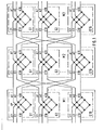
- FIG. 1 shows an overview plan of a three-stage switching network for a message switching system.
- Each stage consists of 16 sub-coupling fields.
- the construction system described above lends itself to the realization of such a switching matrix. So you will train the sub-switch modules as plug-in modules and arrange them in magazines sorted by level.
- Each sub-switching matrix consists of 256 coupling points KP arranged in a 16x16 matrix.
- the 16 sub-coupling fields i.e. the 16 plug-in modules G1 to G16 of a stage, are housed in their own magazine, those of the first stage in a first magazine M1, those of the second stage in a second magazine M2 and those of the third stage in a third magazine M3 .
- Plug-in modules can be built from standardized parts, which can be inserted into magazines (also called full inserts).
- a three-stage switching network is described in European patent specification 0 037 882. It requires printed circuit boards that are turned 90 ° and meet with their end faces. This document teaches nothing about any mounting of these circuit boards and their placement in a magazine. A special construction seems to be necessary. In addition, the connections between the individual stages cannot be made arbitrarily. With this known multi-stage switching matrix, the subtasks a) and b3) on which this invention is based cannot be solved.
- FIG. 2 again shows the three magazines M1 to M3, here their mechanical arrangement one above the other.
- the first magazine M1 is located at the top, below that is the second magazine M2 and at the bottom the third magazine M3. They are mechanically connected to one another in a manner not shown.
- the second magazine is therefore adjacent to both the first and the third.
- Each magazine has 16 guide strips F at the top and bottom, into which the plug-in modules are guided. Only the lower guide bars are visible. Of the 48 plug-in modules (16 per magazine), only the sixteenth plug-in module G16 of the third magazine M3 is shown. Each plug-in module carries a first and a second plug strip S1 or S2 as plug connectors.
- first and a second backplane circuit board L1 and L2 are shown. Each carries two rows of 16 socket strips as mating connectors, with socket strips B1 to B16 forming the upper row and socket strips B17 to B32 forming the lower row. The socket strip B17 and some other socket strips, not shown, are not visible here.
- a third and a fourth backplane L3 and L4 are also provided. These only carry a row of 16 socket strips each.
- Dashed lines indicate in which of the guide strips the plug-in module G16 shown is inserted when it is plugged in, the position of the backplane on the back of the magazine after assembly and that the plug-in strips S1 and S2 of the plug-in module G16 shown in the socket strip B32 of the second Backplane PCB L2 and engage in an unspecified socket strip of the fourth backplane L4.
- the plug strips of the plug-in modules, not shown engage in the socket strips assigned to them. This results in an assignment according to the following table 2:
- the backplane circuit board L1 thus comprises the area of the connector strips S2 of the first magazine M1 and the area of the connector strips S1 of the second magazine M2.
- the area of the connector strips S2 of the first magazine M1 is adjacent to the area of the connector strips S1 of the second magazine M2. The same applies analogously to the backplane L2.
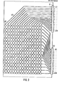
- FIG. 3 shows one of the plug-in modules G1 to G16. It consists of a printed circuit board LP which bears the sub-switching matrix consisting of 256 switching points KP arranged in a 16x16 matrix, a first connector strip S1 and a second connector strip S2.
- the printed circuit board LP has conductor tracks LB which connect the coupling points KP to one another and the 16 inputs E1 to E16 and the 16 outputs A1 to A16 of the sub-switching matrix to the plug strips S1 and S2.
- the inputs E1 to E16 are all on the first connector S1, the outputs A1 to A16 are all led out on the second connector S2.
- the first connector strip S1 is closest to the first magazine M1. Therefore, the inputs E1 to E16 are brought out on it, because they have to be connected to the outputs of the first magazine M1 according to FIG. The same applies analogously to the second connector afford S2 and for the plug-in modules of the other magazines.
- the conductor tracks LB were shown here as single-pole. However, since switching matrixes are usually made with two or even four wires, you have to imagine two or four conductor tracks instead of a line and a corresponding number of connector pins on the connector strips.
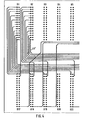
- FIGS. 4 and 6 one of the backplane circuit boards L1 and L2 is shown. Place these figures next to each other, Figure 4 on the left and Figure 6 on the right. The respective upper and lower lines and the left and right lines on FIGS. 4 and 6 indicate the outlines of this backplane.
- B1 to B16 (top row) and B17 to B32 denote the locations for the socket strips B1 to B32. These socket strips themselves are not shown, but only the pads for their soldering pins are indicated by dots.
- the outputs A1 to A16 of the plug-in modules G1 to G16 from the first magazine M1 lie on the socket strips B1 to B16, as can be seen from FIGS. 2 and 3.
- the inputs E1 to E16 of the plug-in modules of the second magazine M2 are located on the socket strips B17 to B32, starting at the top with E1 and A1.
- connections to be created according to Table 1 are formed by conductor tracks LB '.
- a single-pole display was chosen here again; and one has to imagine two conductor tracks instead of a line, since, as can be seen from the representation of two pads for each input and output, here a backplane for a two-wire switching matrix is drawn. Only a few of the many connections to be created according to Table 1 are shown here. In addition, it is not shown that the conductor tracks are distributed over different levels of a multilayer board in order to accommodate their large number and to be able to cross them.
- the second backplane is designed like the first, since according to Table 1 the scheme of the connections between the first and the second stage is the same as that of the connections between the second and third stages.
- the connections produced in this way have electrical properties (e.g. crosstalk attenuation) with little manufacturing variation, and as a result the connections are also suitable for transmitting higher-frequency message signals.
- electrical properties e.g. crosstalk attenuation
- the possible mechanical manufacturing processes of such printed circuit boards also rule out errors due to human error.
- FIG. 7 shows a section through a multilayer plate in order to show the position of the conductor tracks in it. It has nine layers, between which the hatched conductor tracks lie.
- a two-wire switching matrix is assumed, i.e. each connection is designed as a pair of conductor tracks.
- the first pair is labeled LB1 and lies on the first level between the first and second layers.
- the second pair LB2 is not arranged in the next level immediately next to the first pair LB1, but is laterally offset in accordance with the crosstalk attenuation requirement. This transfer extends over four levels.
- the given crosstalk attenuation requirements only make it possible to arrange a pair LB3 again in the fifth level without displacement relative to the first pair LB1.
- the construction system according to the invention is particularly well suited for the construction of broadband switching networks in broadband communication systems in which, among other things, digitized television signals are transmitted at high bit rates. Due to the further development according to claim 2, it is also suitable for communication systems with bit rates of 140 Mbit / s.
- the plug-in modules and magazines of the assembly system according to the invention can be produced from the standardized and commercially available parts of the Intermas assembly system, so that no special designs are required.
- the production of the backplane circuit boards does not pose any new problems either, since they are no larger than those that are common in the Intermas assembly system.
Landscapes
- Engineering & Computer Science (AREA)
- Microelectronics & Electronic Packaging (AREA)
- Physics & Mathematics (AREA)
- Electromagnetism (AREA)
- Computer Networks & Wireless Communication (AREA)
- Details Of Connecting Devices For Male And Female Coupling (AREA)
- Electrotherapy Devices (AREA)
- Organic Insulating Materials (AREA)
- Structure Of Telephone Exchanges (AREA)
- Coupling Device And Connection With Printed Circuit (AREA)
- Metal-Oxide And Bipolar Metal-Oxide Semiconductor Integrated Circuits (AREA)
Priority Applications (1)
| Application Number | Priority Date | Filing Date | Title |
|---|---|---|---|
| AT85112837T ATE39398T1 (de) | 1985-01-24 | 1985-10-10 | Aufbausystem fuer geraete der elektrischen nachrichtentechnik. |
Applications Claiming Priority (2)
| Application Number | Priority Date | Filing Date | Title |
|---|---|---|---|
| DE3502295 | 1985-01-24 | ||
| DE19853502295 DE3502295A1 (de) | 1985-01-24 | 1985-01-24 | Aufbausystem fuer geraete der elektrischen nachrichtentechnik |
Publications (2)
| Publication Number | Publication Date |
|---|---|
| EP0191902A1 true EP0191902A1 (fr) | 1986-08-27 |
| EP0191902B1 EP0191902B1 (fr) | 1988-12-21 |
Family
ID=6260642
Family Applications (1)
| Application Number | Title | Priority Date | Filing Date |
|---|---|---|---|
| EP85112837A Expired EP0191902B1 (fr) | 1985-01-24 | 1985-10-10 | Système de structure pour des appareils de la technique d'informations électriques |
Country Status (6)
| Country | Link |
|---|---|
| US (1) | US4679121A (fr) |
| EP (1) | EP0191902B1 (fr) |
| AT (1) | ATE39398T1 (fr) |
| CA (1) | CA1247223A (fr) |
| DE (2) | DE3502295A1 (fr) |
| DK (1) | DK161276C (fr) |
Cited By (2)
| Publication number | Priority date | Publication date | Assignee | Title |
|---|---|---|---|---|
| EP0240580A1 (fr) * | 1986-04-03 | 1987-10-14 | ANT Nachrichtentechnik GmbH | Dispositif de couplage à trois étages |
| US4862161A (en) * | 1985-01-24 | 1989-08-29 | Ant Nachrichtentechnik Gmbh | Three-stage coupling arrangement |
Families Citing this family (23)
| Publication number | Priority date | Publication date | Assignee | Title |
|---|---|---|---|---|
| US4742477A (en) * | 1984-08-20 | 1988-05-03 | Sci Systems, Inc. | Computer terminal controller and method |
| US4777615A (en) * | 1986-02-28 | 1988-10-11 | Scientific Computer Systems Corporation | Backplane structure for a computer superpositioning scalar and vector operations |
| US5218519A (en) * | 1987-09-08 | 1993-06-08 | Digital Equipment Corporation | Card cage system |
| DE3733264C1 (de) * | 1987-10-01 | 1989-03-30 | Moestronik Unisel Elektronisch | Elektronische Einrichtung |
| US4918335A (en) * | 1987-11-06 | 1990-04-17 | Ford Aerospace Corporation | Interconnection system for integrated circuit chips |
| WO1989007349A1 (fr) * | 1988-02-05 | 1989-08-10 | Commodore-Amiga, Inc. | Connecteur universel |
| US4954949A (en) * | 1988-02-05 | 1990-09-04 | Commodore-Amiga, Inc. | Universal connector device for bus networks in host computer/co-processor computer system |
| US5028809A (en) * | 1989-03-07 | 1991-07-02 | Hewlett-Packard Company | Computer bus structure permitting replacement of modules during operation |
| US5243493A (en) * | 1992-04-29 | 1993-09-07 | Industrial Technology Research Institute | Fanless convection cooling design for personal computers |
| US5227957A (en) * | 1992-05-14 | 1993-07-13 | Deters John B | Modular computer system with passive backplane |
| US5483229A (en) * | 1993-02-18 | 1996-01-09 | Yokogawa Electric Corporation | Input-output unit |
| US5442520A (en) * | 1994-07-01 | 1995-08-15 | Cincinnnati Milacron Inc. | Apparatus for printed circuit board connection |
| US5838533A (en) * | 1997-03-19 | 1998-11-17 | Eaton Corporation | Housing assembly for circuit components |
| US5991163A (en) * | 1998-11-12 | 1999-11-23 | Nexabit Networks, Inc. | Electronic circuit board assembly and method of closely stacking boards and cooling the same |
| US11042211B2 (en) | 2009-08-07 | 2021-06-22 | Advanced Processor Architectures, Llc | Serially connected computing nodes in a distributed computing system |
| US9429983B1 (en) | 2013-09-12 | 2016-08-30 | Advanced Processor Architectures, Llc | System clock distribution in a distributed computing environment |
| US9645603B1 (en) | 2013-09-12 | 2017-05-09 | Advanced Processor Architectures, Llc | System clock distribution in a distributed computing environment |
| US8022526B2 (en) | 2009-08-07 | 2011-09-20 | Advanced Processor Architectures, Llc | Distributed computing |
| US8755197B1 (en) * | 2010-12-31 | 2014-06-17 | Veetle, Inc. | High-density, low-power computer cluster for video streaming |
| US9924609B2 (en) * | 2015-07-24 | 2018-03-20 | Transtector Systems, Inc. | Modular protection cabinet with flexible backplane |
| US10356928B2 (en) | 2015-07-24 | 2019-07-16 | Transtector Systems, Inc. | Modular protection cabinet with flexible backplane |
| US10588236B2 (en) * | 2015-07-24 | 2020-03-10 | Transtector Systems, Inc. | Modular protection cabinet with flexible backplane |
| JP7041085B2 (ja) * | 2019-02-05 | 2022-03-23 | ファナック株式会社 | 電子装置 |
Citations (6)
| Publication number | Priority date | Publication date | Assignee | Title |
|---|---|---|---|---|
| US3798762A (en) * | 1972-08-14 | 1974-03-26 | Us Army | Circuit board processing |
| US3808505A (en) * | 1973-03-19 | 1974-04-30 | Gte Automatic Electric Lab Inc | Apparatus for interconnecting a plurality of electronic equipment frames |
| DE2304456A1 (de) * | 1973-01-30 | 1974-08-01 | Siemens Ag | Einschubsystem fuer elektronikbaugruppen |
| US3923360A (en) * | 1973-03-26 | 1975-12-02 | Cii Honeywell Bull | Multilayer electrical connection panel with modifiable internal circuits |
| US4016463A (en) * | 1973-10-17 | 1977-04-05 | Amdahl Corporation | High density multilayer printed circuit card assembly and method |
| DE2615642A1 (de) * | 1976-04-08 | 1977-10-20 | Licentia Gmbh | Einschub |
Family Cites Families (8)
| Publication number | Priority date | Publication date | Assignee | Title |
|---|---|---|---|---|
| GB806835A (en) * | 1955-03-31 | 1958-12-31 | Standard Telephones Cables Ltd | Improvements in or relating to electronic equipment practice |
| US3179904A (en) * | 1962-12-05 | 1965-04-20 | Ibm | Flexible multiconductor transmission line utilizing alternate conductors as crosstalk shields |
| US3715629A (en) * | 1967-04-05 | 1973-02-06 | Amp Inc | Wiring device for interconnecting module circuit units |
| US3539873A (en) * | 1967-10-19 | 1970-11-10 | Clare & Co C P | Matrix board apparatus |
| US3623127A (en) * | 1969-11-03 | 1971-11-23 | Ashley C Glenn | Electrical printed circuit switching device |
| DE7215350U (de) * | 1972-04-21 | 1972-07-27 | Siemens Ag | Aufnahmevorrichtung für Steckbaugruppen |
| DE3165314D1 (en) * | 1980-04-14 | 1984-09-13 | Grundig Emv | Multi-stage coupling field |
| SE423777B (sv) * | 1980-09-29 | 1982-05-24 | Asea Ab | Elektrisk utrustning innefattande ett antal samarbetande kretskort |
-
1985
- 1985-01-24 DE DE19853502295 patent/DE3502295A1/de not_active Withdrawn
- 1985-10-10 DE DE8585112837T patent/DE3566941D1/de not_active Expired
- 1985-10-10 EP EP85112837A patent/EP0191902B1/fr not_active Expired
- 1985-10-10 AT AT85112837T patent/ATE39398T1/de active
-
1986
- 1986-01-22 CA CA000500104A patent/CA1247223A/fr not_active Expired
- 1986-01-23 DK DK034686A patent/DK161276C/da active
- 1986-01-24 US US06/864,418 patent/US4679121A/en not_active Expired - Lifetime
Patent Citations (6)
| Publication number | Priority date | Publication date | Assignee | Title |
|---|---|---|---|---|
| US3798762A (en) * | 1972-08-14 | 1974-03-26 | Us Army | Circuit board processing |
| DE2304456A1 (de) * | 1973-01-30 | 1974-08-01 | Siemens Ag | Einschubsystem fuer elektronikbaugruppen |
| US3808505A (en) * | 1973-03-19 | 1974-04-30 | Gte Automatic Electric Lab Inc | Apparatus for interconnecting a plurality of electronic equipment frames |
| US3923360A (en) * | 1973-03-26 | 1975-12-02 | Cii Honeywell Bull | Multilayer electrical connection panel with modifiable internal circuits |
| US4016463A (en) * | 1973-10-17 | 1977-04-05 | Amdahl Corporation | High density multilayer printed circuit card assembly and method |
| DE2615642A1 (de) * | 1976-04-08 | 1977-10-20 | Licentia Gmbh | Einschub |
Non-Patent Citations (1)
| Title |
|---|
| ELONCO BULLETIN, Nr. 68, September 1971, Seiten 2-13,, Philips, Eindhoven, NL; "Moderne verbindingstechnieken" * |
Cited By (2)
| Publication number | Priority date | Publication date | Assignee | Title |
|---|---|---|---|---|
| US4862161A (en) * | 1985-01-24 | 1989-08-29 | Ant Nachrichtentechnik Gmbh | Three-stage coupling arrangement |
| EP0240580A1 (fr) * | 1986-04-03 | 1987-10-14 | ANT Nachrichtentechnik GmbH | Dispositif de couplage à trois étages |
Also Published As
| Publication number | Publication date |
|---|---|
| DE3502295A1 (de) | 1986-07-24 |
| DK34686A (da) | 1986-07-25 |
| DK161276B (da) | 1991-06-17 |
| EP0191902B1 (fr) | 1988-12-21 |
| US4679121A (en) | 1987-07-07 |
| DE3566941D1 (en) | 1989-01-26 |
| DK161276C (da) | 1991-12-09 |
| ATE39398T1 (de) | 1989-01-15 |
| CA1247223A (fr) | 1988-12-20 |
| DK34686D0 (da) | 1986-01-23 |
Similar Documents
| Publication | Publication Date | Title |
|---|---|---|
| EP0191902B1 (fr) | Système de structure pour des appareils de la technique d'informations électriques | |
| EP0712267B1 (fr) | Installation de commande modulaire avec connexion sur bus secteur intégré | |
| DE3740568C2 (fr) | ||
| DE69214289T2 (de) | Elektrisches verbindungssystem | |
| DE2432441A1 (de) | Kreuzverbindungsschalter | |
| DE2130637A1 (de) | Elektronischer Baustein und aus mehreren solcher Bausteine gebildete Schaltungsanordnung | |
| DE2349444A1 (de) | Steckkontaktschalter | |
| DE3836360A1 (de) | Verteilereinrichtung, insbesondere fuer den hauptverteiler von fernsprechanlagen | |
| EP3562283A1 (fr) | Arrangement modulaire backplane | |
| EP0222030A1 (fr) | Bloc de connexion pour initiateur | |
| DE3511344A1 (de) | Steckverbinder fuer rueckwandverdrahtungen | |
| DE2644296A1 (de) | Dreireihiger leitungsstecker mit sogenannten kontaktgabeln zum anschliessen von flachbandkabeln | |
| DE2214503A1 (de) | Aufnahmevorrichtung zur aufnahme von gehaeusen fuer die elektrische nachrichtenuebertragungstechnik | |
| EP0270185B1 (fr) | Champ multiplage à large bande à interconnexions portées par une plaque à conducteurs en couches multiples en technique "microstrip" | |
| EP0240580B2 (fr) | Dispositif de couplage à trois étages | |
| DE2901678B1 (de) | Verteiler fuer kleine Fernsprechvermittlungsanlagen | |
| DE3736025C1 (en) | Multiple plug connector | |
| DE3249507T1 (de) | Reihen- oder schichtenweise angeordnete, senkrecht zueinander in Bezug stehende, drei dimensionale gedruckte Plattenschaltung | |
| EP1503307A1 (fr) | Appareil pour la emulation de conceptions des circuits integrés | |
| DE8908973U1 (de) | Eine aus mindestens aus zwei parallel zueinander angeordneten Leiterplatten bestehende Baugruppe mit elektrisch leitender Verbindung | |
| EP0199309A2 (fr) | Elément multiple de raccordement pour connecter une pluralité de terminaux multiples | |
| DE3435773A1 (de) | Rueckwandverdrahtung fuer einschiebbare elektrische baugruppen | |
| DE2247523A1 (de) | Elektrische oder elektronische koppelanordnung fuer fernmelde-, insbesondere fernsprechvermittlungsanlagen | |
| EP0865121A1 (fr) | Connecteur-adapteur pour la connection d'une connecteur à 4 pÔles à un connecteur à 8 pÔles selon la norme RJ45 | |
| WO2016162017A1 (fr) | Module de connexion pour connecteur modulaire |
Legal Events
| Date | Code | Title | Description |
|---|---|---|---|
| PUAI | Public reference made under article 153(3) epc to a published international application that has entered the european phase |
Free format text: ORIGINAL CODE: 0009012 |
|
| AK | Designated contracting states |
Kind code of ref document: A1 Designated state(s): AT BE DE FR GB IT NL SE |
|
| 17P | Request for examination filed |
Effective date: 19860911 |
|
| 17Q | First examination report despatched |
Effective date: 19880504 |
|
| GRAA | (expected) grant |
Free format text: ORIGINAL CODE: 0009210 |
|
| AK | Designated contracting states |
Kind code of ref document: B1 Designated state(s): AT BE DE FR GB IT NL SE |
|
| ITF | It: translation for a ep patent filed | ||
| REF | Corresponds to: |
Ref document number: 39398 Country of ref document: AT Date of ref document: 19890115 Kind code of ref document: T |
|
| GBT | Gb: translation of ep patent filed (gb section 77(6)(a)/1977) | ||
| REF | Corresponds to: |
Ref document number: 3566941 Country of ref document: DE Date of ref document: 19890126 |
|
| ET | Fr: translation filed | ||
| PLBE | No opposition filed within time limit |
Free format text: ORIGINAL CODE: 0009261 |
|
| STAA | Information on the status of an ep patent application or granted ep patent |
Free format text: STATUS: NO OPPOSITION FILED WITHIN TIME LIMIT |
|
| 26N | No opposition filed | ||
| ITTA | It: last paid annual fee | ||
| PGFP | Annual fee paid to national office [announced via postgrant information from national office to epo] |
Ref country code: NL Payment date: 19931031 Year of fee payment: 9 |
|
| EAL | Se: european patent in force in sweden |
Ref document number: 85112837.1 |
|
| PG25 | Lapsed in a contracting state [announced via postgrant information from national office to epo] |
Ref country code: NL Effective date: 19950501 |
|
| NLV4 | Nl: lapsed or anulled due to non-payment of the annual fee | ||
| PGFP | Annual fee paid to national office [announced via postgrant information from national office to epo] |
Ref country code: GB Payment date: 20000927 Year of fee payment: 16 |
|
| PGFP | Annual fee paid to national office [announced via postgrant information from national office to epo] |
Ref country code: SE Payment date: 20001009 Year of fee payment: 16 |
|
| PGFP | Annual fee paid to national office [announced via postgrant information from national office to epo] |
Ref country code: FR Payment date: 20001010 Year of fee payment: 16 |
|
| PGFP | Annual fee paid to national office [announced via postgrant information from national office to epo] |
Ref country code: AT Payment date: 20001011 Year of fee payment: 16 |
|
| PGFP | Annual fee paid to national office [announced via postgrant information from national office to epo] |
Ref country code: BE Payment date: 20001214 Year of fee payment: 16 |
|
| PG25 | Lapsed in a contracting state [announced via postgrant information from national office to epo] |
Ref country code: GB Free format text: LAPSE BECAUSE OF NON-PAYMENT OF DUE FEES Effective date: 20011010 Ref country code: AT Free format text: LAPSE BECAUSE OF NON-PAYMENT OF DUE FEES Effective date: 20011010 |
|
| PG25 | Lapsed in a contracting state [announced via postgrant information from national office to epo] |
Ref country code: SE Free format text: LAPSE BECAUSE OF NON-PAYMENT OF DUE FEES Effective date: 20011011 |
|
| PGFP | Annual fee paid to national office [announced via postgrant information from national office to epo] |
Ref country code: DE Payment date: 20011022 Year of fee payment: 17 |
|
| PG25 | Lapsed in a contracting state [announced via postgrant information from national office to epo] |
Ref country code: BE Free format text: LAPSE BECAUSE OF NON-PAYMENT OF DUE FEES Effective date: 20011031 |
|
| REG | Reference to a national code |
Ref country code: GB Ref legal event code: IF02 |
|
| BERE | Be: lapsed |
Owner name: ANT NACHRICHTENTECHNIK G.M.B.H. Effective date: 20011031 |
|
| GBPC | Gb: european patent ceased through non-payment of renewal fee |
Effective date: 20011010 |
|
| EUG | Se: european patent has lapsed |
Ref document number: 85112837.1 |
|
| PG25 | Lapsed in a contracting state [announced via postgrant information from national office to epo] |
Ref country code: FR Free format text: LAPSE BECAUSE OF NON-PAYMENT OF DUE FEES Effective date: 20020628 |
|
| REG | Reference to a national code |
Ref country code: FR Ref legal event code: ST |
|
| PG25 | Lapsed in a contracting state [announced via postgrant information from national office to epo] |
Ref country code: DE Free format text: LAPSE BECAUSE OF NON-PAYMENT OF DUE FEES Effective date: 20030501 |