EP0192256A2 - Magnetooptischer Informationsträger - Google Patents
Magnetooptischer Informationsträger Download PDFInfo
- Publication number
- EP0192256A2 EP0192256A2 EP86102161A EP86102161A EP0192256A2 EP 0192256 A2 EP0192256 A2 EP 0192256A2 EP 86102161 A EP86102161 A EP 86102161A EP 86102161 A EP86102161 A EP 86102161A EP 0192256 A2 EP0192256 A2 EP 0192256A2
- Authority
- EP
- European Patent Office
- Prior art keywords
- nickel
- aluminium
- storage element
- thin film
- magnetooptical storage
- Prior art date
- Legal status (The legal status is an assumption and is not a legal conclusion. Google has not performed a legal analysis and makes no representation as to the accuracy of the status listed.)
- Granted
Links
Images

Classifications
-
- G—PHYSICS
- G11—INFORMATION STORAGE
- G11B—INFORMATION STORAGE BASED ON RELATIVE MOVEMENT BETWEEN RECORD CARRIER AND TRANSDUCER
- G11B7/00—Recording or reproducing by optical means, e.g. recording using a thermal beam of optical radiation by modifying optical properties or the physical structure, reproducing using an optical beam at lower power by sensing optical properties; Record carriers therefor
- G11B7/24—Record carriers characterised by shape, structure or physical properties, or by the selection of the material
- G11B7/26—Apparatus or processes specially adapted for the manufacture of record carriers
-
- G—PHYSICS
- G11—INFORMATION STORAGE
- G11B—INFORMATION STORAGE BASED ON RELATIVE MOVEMENT BETWEEN RECORD CARRIER AND TRANSDUCER
- G11B11/00—Recording on or reproducing from the same record carrier wherein for these two operations the methods are covered by different main groups of groups G11B3/00 - G11B7/00 or by different subgroups of group G11B9/00; Record carriers therefor
- G11B11/10—Recording on or reproducing from the same record carrier wherein for these two operations the methods are covered by different main groups of groups G11B3/00 - G11B7/00 or by different subgroups of group G11B9/00; Record carriers therefor using recording by magnetic means or other means for magnetisation or demagnetisation of a record carrier, e.g. light induced spin magnetisation; Demagnetisation by thermal or stress means in the presence or not of an orienting magnetic field
- G11B11/105—Recording on or reproducing from the same record carrier wherein for these two operations the methods are covered by different main groups of groups G11B3/00 - G11B7/00 or by different subgroups of group G11B9/00; Record carriers therefor using recording by magnetic means or other means for magnetisation or demagnetisation of a record carrier, e.g. light induced spin magnetisation; Demagnetisation by thermal or stress means in the presence or not of an orienting magnetic field using a beam of light or a magnetic field for recording by change of magnetisation and a beam of light for reproducing, i.e. magneto-optical, e.g. light-induced thermomagnetic recording, spin magnetisation recording, Kerr or Faraday effect reproducing
- G11B11/10582—Record carriers characterised by the selection of the material or by the structure or form
- G11B11/10586—Record carriers characterised by the selection of the material or by the structure or form characterised by the selection of the material
- G11B11/10589—Details
-
- Y—GENERAL TAGGING OF NEW TECHNOLOGICAL DEVELOPMENTS; GENERAL TAGGING OF CROSS-SECTIONAL TECHNOLOGIES SPANNING OVER SEVERAL SECTIONS OF THE IPC; TECHNICAL SUBJECTS COVERED BY FORMER USPC CROSS-REFERENCE ART COLLECTIONS [XRACs] AND DIGESTS
- Y10—TECHNICAL SUBJECTS COVERED BY FORMER USPC
- Y10S—TECHNICAL SUBJECTS COVERED BY FORMER USPC CROSS-REFERENCE ART COLLECTIONS [XRACs] AND DIGESTS
- Y10S428/00—Stock material or miscellaneous articles
- Y10S428/90—Magnetic feature
-
- Y—GENERAL TAGGING OF NEW TECHNOLOGICAL DEVELOPMENTS; GENERAL TAGGING OF CROSS-SECTIONAL TECHNOLOGIES SPANNING OVER SEVERAL SECTIONS OF THE IPC; TECHNICAL SUBJECTS COVERED BY FORMER USPC CROSS-REFERENCE ART COLLECTIONS [XRACs] AND DIGESTS
- Y10—TECHNICAL SUBJECTS COVERED BY FORMER USPC
- Y10S—TECHNICAL SUBJECTS COVERED BY FORMER USPC CROSS-REFERENCE ART COLLECTIONS [XRACs] AND DIGESTS
- Y10S428/00—Stock material or miscellaneous articles
- Y10S428/922—Static electricity metal bleed-off metallic stock
- Y10S428/9265—Special properties
- Y10S428/928—Magnetic property
-
- Y—GENERAL TAGGING OF NEW TECHNOLOGICAL DEVELOPMENTS; GENERAL TAGGING OF CROSS-SECTIONAL TECHNOLOGIES SPANNING OVER SEVERAL SECTIONS OF THE IPC; TECHNICAL SUBJECTS COVERED BY FORMER USPC CROSS-REFERENCE ART COLLECTIONS [XRACs] AND DIGESTS
- Y10—TECHNICAL SUBJECTS COVERED BY FORMER USPC
- Y10T—TECHNICAL SUBJECTS COVERED BY FORMER US CLASSIFICATION
- Y10T428/00—Stock material or miscellaneous articles
- Y10T428/31504—Composite [nonstructural laminate]
- Y10T428/31678—Of metal
Definitions
- the present invention generally relates to storage elements and more particularly, to a magnetooptical storage element in which recording, reproduction, erasure, etc. of data are performed by irradiating laser beams, etc. thereto.
- magnetooptical storage elements have been greatly developed as optical memory elements enabling recording, reproduction and erasure of data.
- a magnetooptical storage element in which a thin film made of an amorphous alloy containing rare-earth transition metals is used as a storage medium has such advantages that a recorded bit is not affected by the grain boundary and the film of the storage medium can be manufactured over a large area relatively easily, thereby attracting special attention.
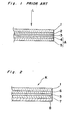
- Fig. 1 shows a prior art magnetooptical storage element having the reflective film construction.
- the prior art magnetooptical storage element includes a transparent substrate 1, a transparent dielectric film 2 having a refractive index higher than that of the substrate 1, a thin film 3 made of an amorphous alloy containing rare-earth transition metals, a transparent dielectric film 4 and a metallic reflective film 5.
- the thin film 3 has a sufficiently small thickness.
- the substrate 1 is formed by a glass plate, while the dielectric film 2 is made of SiO so as to have a thickness of 120 nm. Furthermore, the thin film 3 is made of Gd-Tb-Fe alloy so as to have a thickness of 15 nm, while the dielectric film 4 is made of Si0 2 so as to have a thickness of 50 nm. Meanwhile, the reflective film 5 is made of Cu so as to have a thickness of 50 nm. In this example of the known magnetooptical storage element, the Kerr rotational angle increased to 1.75° superficially.
- the Kerr rotational angle increases extraordinarily in the magnetooptical storage element of the above described construction.
- the laser beam L is irradiated onto the thin film 3 from the substrate 1 as shown in Fig. 1
- reflection of the incident laser beam L is repeated in the dielectric film 2, so that interference of the repeatedly reflected laser beam L takes place and thus, the Kerr rotational angle increases superficially.
- the dielectric film 2 further contributes to increase of the Kerr rotational angle.
- an arrangement in which the reflective film 5 is disposed rearwardly of the thin film 3 also increases the Kerr rotational angle superficially. By interposing the dielectric film 4 between the thin film 3 and the reflective film 5, the Kerr rotational angle is further increased superficially.
- a reflective layer A is constituted by the dielectric film 4 and the reflective film 5.
- a first light ray incident upon the thin film 3 from the substrate 1 is reflected on the reflective layer A after passing through the thin film 3 and then, reversely passes through the thin film 3 again.
- a second light ray incident upon the thin film 3 from the substrate 1 is directly reflected on the surface of the thin film 3 without passing through the thin film 3. Therefore, the first light ray which has passed through the thin film 3 reversely upon its reflection on the reflective layer A and the second light ray which has been reflected on the surface of the thin film 3 are combined with each other.
- the thin film 3 is increased in thickness, the rotational angle can be increased.
- a proper thickness of the thin film 3 ranges from approximately 10 to 50 nm and is determined based on wave length of the laser beam L, refractive index of the reflective layer A, etc.
- a requirement for the reflective layer A is that the reflective layer A should have a high refractive index.
- the Kerr rotational angle can be increased effectively.
- a requirement for the reflective film 5 is that the reflective film 5 should have a high refractive index.
- the reflective film 5 is made of one of such materials as Au, Ag, Cu, At, etc.
- these materials of the reflective film 5 undesirably lower recording sensitivity of the storage medium due to their excellent thermal conductivity.
- recording of data is performed by inverting orientation of magnetization through not only local heating of the storage medium by the use of laser beams but application of an auxiliary magnetic field to the storage medium from its outside.
- the material of the reflective film has excellent thermal conductivity, heat given to the storage medium at the time of recording of the data is instantaneously diffused and thus, temperature of the storage medium cannot be raised sufficiently to a required level.
- the reflective film 5 is required to have not only a high refractive index but a low coefficient of thermal conductivity.
- the above described materials such as Ai, Cu, AG and Au for the reflective film 5 are of high refractive indexes but have high coefficients of thermal conductivity. Therefore, the reflective film 5 made of one of the materials such as At, Cu, Ag and Au is capable of improving quality of reproduced signals but disadvantageously lowers recording sensitivity of the storage medium.
- an essential object of the present invention is to provide a magnetooptical storage element in which reproduced signals are improved in quality without drop of its recording sensitivity, with substantial elimination of the disadvantages inherent in conventional magnetooptical storage elements of this kind.
- a magnetooptical storage element embodying the present invention comprises a reflective layer made of an alloy containing aluminium and one of elements for lowering a coefficient of thermal conductivity of aluminium, which elements include nickel, palladium, platinum, chromium and molybdenum.
- the magnetooptical storage element K includes a transparent substrate 1 made of glass, polycarbonate, acrylic material or the like, a first transparent dielectric film 6 having a thickness of, for example, 100 nm and made of aluminium nitride (AlN), a thin film 3 having a thickness of, for example, 27 nm and made of an amorphous alloy containing rare-earth transition metals, a second transparent dielectric film 7 having a thickness of, for example, 35 nm and made of aluminium nitride (AiN), and a reflective film 8 having a thickness of, for example, not less than 30 nm, which are sequentially piled one on another in this order.
- the thin film 3 is made of, for example, Gd-Tb-Fe alloy.
- the reflective film 8 is made of an alloy containing aluminium and one of elements for lowering a coefficient of thermal conductivity of aluminium, which elements include nickel, palladium, platinum, chromium and molybdenum.
- nickel is employed as one of the elements for lowering the coefficient of thermal conductivity of aluminium.
- a target obtained by adding nickel to aluminium is sputtered.
- the reflective film 8 is made of At-Ni alloy as described above, the following advantage is achieved. Namely, aluminium has a high coefficient of thermal conductivity as referred to earlier.
- the reflective film 8 when the reflective film 8 is made of aluminium, aluminium acts as a heat sink at the time of thermomagnetic recording by the use of laser beams, etc., so that such phenomena as drop of recording sensitivity or drop of recording speed may take place.
- a coefficient of thermal conductivity of the Ai-Ni alloy is smaller than that of aluminium itself. Therefore, when the reflective film 8 is made of the At-Ni alloy, recording sensitivity is considerably improved as compared with that in the case where the reflective film 8 is made of aluminium only.
- Fig. 3 is a graph indicative of relation among composition of nickel in the Ai-Ni alloy of the reflective film 8, recording sensitivity and carrier-to-noise (C/N) ratio representing quality of reproduced signals.
- the recording sensitivity is expressed by length of a bit recorded at the time when laser beams having a predetermined amount of energy have been irradiated for a fixed time period. Namely, the recording sensitivity is deemed to be higher when the recorded bit becomes larger in length.
- curves P and Q represent the length of the recorded bit (recording sensitivity) and the C/N ratio, respectively. It will be readily seen from Fig. 3 that as composition of nickel is increased in the Al-Ni alloy constituting the reflective film 8, the recording sensitivity is improved. Meanwhile, in this case, the C/N ratio drops on the contrary.
- Table 1 shows change of refractive index of the Ai-Ni alloy versus change of composition (atomic %) of nickel in the Al-Ni alloy. It is to be noted that characters n and k in Table 1 represent real part and imaginary part of the refractive index of the Al-Ni alloy, respectively.
Landscapes
- Engineering & Computer Science (AREA)
- Manufacturing & Machinery (AREA)
Applications Claiming Priority (2)
| Application Number | Priority Date | Filing Date | Title |
|---|---|---|---|
| JP60034133A JPH0697514B2 (ja) | 1985-02-21 | 1985-02-21 | 磁気光学記憶素子 |
| JP34133/85 | 1985-02-21 |
Publications (3)
| Publication Number | Publication Date |
|---|---|
| EP0192256A2 true EP0192256A2 (de) | 1986-08-27 |
| EP0192256A3 EP0192256A3 (en) | 1988-11-30 |
| EP0192256B1 EP0192256B1 (de) | 1992-05-13 |
Family
ID=12405722
Family Applications (1)
| Application Number | Title | Priority Date | Filing Date |
|---|---|---|---|
| EP86102161A Expired - Lifetime EP0192256B1 (de) | 1985-02-21 | 1986-02-19 | Magnetooptischer Informationsträger |
Country Status (5)
| Country | Link |
|---|---|
| US (1) | US4717628A (de) |
| EP (1) | EP0192256B1 (de) |
| JP (1) | JPH0697514B2 (de) |
| CA (1) | CA1252887A (de) |
| DE (1) | DE3685236D1 (de) |
Cited By (15)
| Publication number | Priority date | Publication date | Assignee | Title |
|---|---|---|---|---|
| US4786559A (en) * | 1985-12-25 | 1988-11-22 | Sharp Kabushiki Kaisha | Magnetooptical storage element |
| EP0288069A3 (en) * | 1987-04-24 | 1989-03-29 | Sony Corporation | Thermomagnetic recording method applying a power modulated laser beam on a magnetically coupled multi-layer structure of a perpendicular anisotropy magnetic film |
| EP0329450A3 (en) * | 1988-02-17 | 1990-01-10 | Victor Company Of Japan, Limited | Optical record medium having an improved reflection thin film |
| EP0317982A3 (en) * | 1987-11-25 | 1990-08-22 | Sony Corporation | Magneto-optical recording medium |
| EP0350010A3 (de) * | 1988-07-07 | 1991-07-10 | Oki Electric Industry Co., Ltd. | Magneto-optisches Speichermedium |
| EP0349271A3 (de) * | 1988-06-28 | 1991-07-17 | Sharp Kabushiki Kaisha | Magneto-optisches Speichergerät |
| EP0368194A3 (de) * | 1988-11-07 | 1992-03-04 | Hitachi, Ltd. | Magneto-optische Anordnung |
| EP0503607A3 (en) * | 1991-03-14 | 1993-02-10 | Tdk Corporation | Magneto-optical recording medium |
| US5486395A (en) * | 1991-12-05 | 1996-01-23 | Sharp Kabushiki Kaisha | Magneto-optical disk |
| EP0331737B1 (de) * | 1987-08-08 | 1996-06-05 | Mitsui Petrochemical Industries, Ltd. | Photomagnetisches speichermedium |
| US5698312A (en) * | 1990-03-22 | 1997-12-16 | Fuji Photo Film Co., Ltd. | Magneto-optical recording medium and method for making the same |
| US5700567A (en) * | 1991-03-14 | 1997-12-23 | Tdk Corporation | Magneto-optical recording medium |
| US5914198A (en) * | 1989-06-05 | 1999-06-22 | Hitachi, Ltd. | Magneto-optical recording medium having dielectric layers with different indices of refraction |
| US6139949A (en) * | 1989-02-10 | 2000-10-31 | Mitsubishi Denki Kabushiki Kaisha | Magneto optical recording medium |
| WO2004105008A1 (ja) | 2003-05-23 | 2004-12-02 | Matsushita Electric Industrial Co., Ltd. | 光学的情報記録媒体及びその製造方法 |
Families Citing this family (15)
| Publication number | Priority date | Publication date | Assignee | Title |
|---|---|---|---|---|
| WO1988003310A1 (fr) * | 1986-10-29 | 1988-05-05 | Dai Nippon Insatsu Kabushiki Kaisha | Support d'enregistrement optique du type draw |
| JP2561130B2 (ja) * | 1988-06-27 | 1996-12-04 | 富士写真フイルム株式会社 | 光磁気記録媒体 |
| JPH02223040A (ja) * | 1988-11-04 | 1990-09-05 | Fuji Photo Film Co Ltd | 光磁気記録媒体 |
| JP2997471B2 (ja) * | 1988-12-05 | 2000-01-11 | 株式会社日立製作所 | 光磁気デイクス |
| US5055353A (en) * | 1989-05-16 | 1991-10-08 | Fuji Photo Film Co., Ltd. | Magneto-optical recording medium |
| JP2654689B2 (ja) * | 1989-05-16 | 1997-09-17 | 富士写真フイルム株式会社 | 光磁気記録媒体 |
| CA2017284C (en) * | 1989-07-04 | 1995-10-03 | Kazutomi Suzuki | Optical recording medium |
| EP0470546B1 (de) * | 1990-08-07 | 1998-11-04 | Hitachi Maxell Ltd. | Magnetooptischer Aufzeichnungsträger |
| JPH04335231A (ja) * | 1991-05-10 | 1992-11-24 | Nec Corp | 光磁気記録用単板光ディスク |
| US5547751A (en) * | 1992-04-10 | 1996-08-20 | Mitsubishi Denki Kabushiki Kaisha | Magneto-optical recording medium and method of manufacturing the same |
| JP3292890B2 (ja) * | 1992-08-10 | 2002-06-17 | 株式会社リコー | 光反射放熱用材料を用いた相変化形光記録媒体 |
| JP2960824B2 (ja) * | 1992-09-30 | 1999-10-12 | ティーディーケイ株式会社 | 光磁気記録媒体 |
| US5948497A (en) * | 1992-10-19 | 1999-09-07 | Eastman Kodak Company | High stability silver based alloy reflectors for use in a writable compact disk |
| US5458941A (en) * | 1994-06-09 | 1995-10-17 | Minnesota Mining And Manufacturing Company | Optical recording medium exhibiting eutectic phase equilbria |
| US6582764B2 (en) * | 2001-10-09 | 2003-06-24 | Engelhard Corporation | Hybrid inorganic/organic color effect materials and production thereof |
Family Cites Families (10)
| Publication number | Priority date | Publication date | Assignee | Title |
|---|---|---|---|---|
| US4467383A (en) * | 1980-02-23 | 1984-08-21 | Sharp Kabushiki Kaisha | Magnetooptic memory medium |
| US4414650A (en) * | 1980-06-23 | 1983-11-08 | Sharp Kabushiki Kaisha | Magneto-optic memory element |
| CA1185013A (en) * | 1981-01-14 | 1985-04-02 | Kenji Ohta | Magneto-optic memory medium |
| NL8102283A (nl) * | 1981-05-11 | 1982-12-01 | Philips Nv | Optisch uitleesbare informatieschijf met een reflectielaag gevormd uit een metaallegering. |
| JPS5860441A (ja) * | 1981-10-06 | 1983-04-09 | Canon Inc | 光熱磁気記録媒体 |
| US4544443A (en) * | 1983-05-13 | 1985-10-01 | Shap Kabushiki Kaisha | Method for manufacturing an optical memory element |
| JPH0636253B2 (ja) * | 1983-08-18 | 1994-05-11 | シャープ株式会社 | 光メモリ円板 |
| CA1224270A (en) * | 1983-09-16 | 1987-07-14 | Junji Hirokane | Magneto-optic memory element |
| US4719137A (en) * | 1984-04-13 | 1988-01-12 | Sharp Kabushiki Kaisha | Magneto-optic memory element |
| JPS60247844A (ja) * | 1984-05-22 | 1985-12-07 | Sharp Corp | 磁気光学記憶素子の製造方法 |
-
1985
- 1985-02-21 JP JP60034133A patent/JPH0697514B2/ja not_active Expired - Lifetime
-
1986
- 1986-02-18 CA CA000502051A patent/CA1252887A/en not_active Expired
- 1986-02-19 DE DE8686102161T patent/DE3685236D1/de not_active Expired - Lifetime
- 1986-02-19 EP EP86102161A patent/EP0192256B1/de not_active Expired - Lifetime
- 1986-02-19 US US06/830,862 patent/US4717628A/en not_active Expired - Lifetime
Cited By (19)
| Publication number | Priority date | Publication date | Assignee | Title |
|---|---|---|---|---|
| US4786559A (en) * | 1985-12-25 | 1988-11-22 | Sharp Kabushiki Kaisha | Magnetooptical storage element |
| EP0288069A3 (en) * | 1987-04-24 | 1989-03-29 | Sony Corporation | Thermomagnetic recording method applying a power modulated laser beam on a magnetically coupled multi-layer structure of a perpendicular anisotropy magnetic film |
| US4878132A (en) * | 1987-04-24 | 1989-10-31 | Sony Corporation | Thermomagnetic recording method applying power modulated laser on a magnetically coupled multi-layer structure of perpendicular anisotropy magnetic film |
| EP0331737B1 (de) * | 1987-08-08 | 1996-06-05 | Mitsui Petrochemical Industries, Ltd. | Photomagnetisches speichermedium |
| EP0317982A3 (en) * | 1987-11-25 | 1990-08-22 | Sony Corporation | Magneto-optical recording medium |
| EP0329450A3 (en) * | 1988-02-17 | 1990-01-10 | Victor Company Of Japan, Limited | Optical record medium having an improved reflection thin film |
| US5058098A (en) * | 1988-02-17 | 1991-10-15 | Victor Company Of Japan, Ltd. | Optical record medium having an improved reflection thin film |
| EP0349271A3 (de) * | 1988-06-28 | 1991-07-17 | Sharp Kabushiki Kaisha | Magneto-optisches Speichergerät |
| EP0350010A3 (de) * | 1988-07-07 | 1991-07-10 | Oki Electric Industry Co., Ltd. | Magneto-optisches Speichermedium |
| EP0368194A3 (de) * | 1988-11-07 | 1992-03-04 | Hitachi, Ltd. | Magneto-optische Anordnung |
| US5654058A (en) * | 1988-11-07 | 1997-08-05 | Hitachi, Ltd. | Magneto-optical disk |
| US6139949A (en) * | 1989-02-10 | 2000-10-31 | Mitsubishi Denki Kabushiki Kaisha | Magneto optical recording medium |
| US5914198A (en) * | 1989-06-05 | 1999-06-22 | Hitachi, Ltd. | Magneto-optical recording medium having dielectric layers with different indices of refraction |
| US5698312A (en) * | 1990-03-22 | 1997-12-16 | Fuji Photo Film Co., Ltd. | Magneto-optical recording medium and method for making the same |
| EP0503607A3 (en) * | 1991-03-14 | 1993-02-10 | Tdk Corporation | Magneto-optical recording medium |
| US5700567A (en) * | 1991-03-14 | 1997-12-23 | Tdk Corporation | Magneto-optical recording medium |
| US5486395A (en) * | 1991-12-05 | 1996-01-23 | Sharp Kabushiki Kaisha | Magneto-optical disk |
| WO2004105008A1 (ja) | 2003-05-23 | 2004-12-02 | Matsushita Electric Industrial Co., Ltd. | 光学的情報記録媒体及びその製造方法 |
| EP1630801A4 (de) * | 2003-05-23 | 2008-03-19 | Matsushita Electric Industrial Co Ltd | Optisches informationsaufzeichnungsmedium und prozess zu seiner herstellung |
Also Published As
| Publication number | Publication date |
|---|---|
| CA1252887A (en) | 1989-04-18 |
| JPS61194664A (ja) | 1986-08-29 |
| EP0192256B1 (de) | 1992-05-13 |
| DE3685236D1 (de) | 1992-06-17 |
| JPH0697514B2 (ja) | 1994-11-30 |
| EP0192256A3 (en) | 1988-11-30 |
| US4717628A (en) | 1988-01-05 |
Similar Documents
| Publication | Publication Date | Title |
|---|---|---|
| EP0192256A2 (de) | Magnetooptischer Informationsträger | |
| EP0139474B1 (de) | Magnetooptisches Speicherelement | |
| US4658388A (en) | Optical recording medium which includes a corrosion resistant film of a mixture of a carbide and a nitride | |
| EP0233034B1 (de) | Element mit optischem Gedächtnis | |
| US5620767A (en) | Light reflecting and heat dissipating material and optical information recording medium using the same | |
| EP0793223B1 (de) | Optisches Aufzeichnungsmedium | |
| EP0228909B1 (de) | Magnetooptisches Speicherelement | |
| EP0387420B1 (de) | Magneto-optischer Aufzeichnungsträger | |
| US4711821A (en) | Opto-magnetic recording medium | |
| US5643650A (en) | Magneto-optical recording medium | |
| JP2908826B2 (ja) | 情報記録媒体 | |
| EP0350010B1 (de) | Magneto-optisches Speichermedium | |
| US5040166A (en) | Magneto-optical recording medium having a reflective film of Ag and Mn or Ag, Mn and Sn | |
| GB2158281A (en) | Optical recording medium | |
| US5667862A (en) | Magneto-optical disk | |
| JP2921590B2 (ja) | 光磁気記録媒体 | |
| JPH0524571B2 (de) | ||
| JPH05303781A (ja) | 光磁気記録媒体 | |
| US5589282A (en) | Magneto-optical recording medium | |
| JPH05185733A (ja) | 情報記録媒体 | |
| JP2912725B2 (ja) | 光磁気記録体 | |
| JPH08175016A (ja) | 相変化型光記録媒体 | |
| JP2678222B2 (ja) | 光磁気記録媒体 | |
| JPH11232694A (ja) | 記録媒体 | |
| JPH06203410A (ja) | 光学情報記録媒体 |
Legal Events
| Date | Code | Title | Description |
|---|---|---|---|
| PUAI | Public reference made under article 153(3) epc to a published international application that has entered the european phase |
Free format text: ORIGINAL CODE: 0009012 |
|
| AK | Designated contracting states |
Kind code of ref document: A2 Designated state(s): DE FR GB IT |
|
| PUAL | Search report despatched |
Free format text: ORIGINAL CODE: 0009013 |
|
| RHK1 | Main classification (correction) |
Ipc: G11B 11/10 |
|
| AK | Designated contracting states |
Kind code of ref document: A3 Designated state(s): DE FR GB IT |
|
| 17P | Request for examination filed |
Effective date: 19881210 |
|
| 17Q | First examination report despatched |
Effective date: 19900509 |
|
| GRAA | (expected) grant |
Free format text: ORIGINAL CODE: 0009210 |
|
| AK | Designated contracting states |
Kind code of ref document: B1 Designated state(s): DE FR GB IT |
|
| REF | Corresponds to: |
Ref document number: 3685236 Country of ref document: DE Date of ref document: 19920617 |
|
| ET | Fr: translation filed | ||
| ITF | It: translation for a ep patent filed | ||
| PLBE | No opposition filed within time limit |
Free format text: ORIGINAL CODE: 0009261 |
|
| STAA | Information on the status of an ep patent application or granted ep patent |
Free format text: STATUS: NO OPPOSITION FILED WITHIN TIME LIMIT |
|
| 26N | No opposition filed | ||
| REG | Reference to a national code |
Ref country code: GB Ref legal event code: IF02 |
|
| PGFP | Annual fee paid to national office [announced via postgrant information from national office to epo] |
Ref country code: FR Payment date: 20050208 Year of fee payment: 20 |
|
| PGFP | Annual fee paid to national office [announced via postgrant information from national office to epo] |
Ref country code: GB Payment date: 20050216 Year of fee payment: 20 |
|
| PGFP | Annual fee paid to national office [announced via postgrant information from national office to epo] |
Ref country code: DE Payment date: 20050217 Year of fee payment: 20 |
|
| PGFP | Annual fee paid to national office [announced via postgrant information from national office to epo] |
Ref country code: IT Payment date: 20050225 Year of fee payment: 20 |
|
| REG | Reference to a national code |
Ref country code: GB Ref legal event code: PE20 |
|
| PG25 | Lapsed in a contracting state [announced via postgrant information from national office to epo] |
Ref country code: GB Free format text: LAPSE BECAUSE OF EXPIRATION OF PROTECTION Effective date: 20060218 |