EP0192366A2 - Appareil et procédé d'amélioration de performances de système-bus dans un système de traitement de données - Google Patents
Appareil et procédé d'amélioration de performances de système-bus dans un système de traitement de données Download PDFInfo
- Publication number
- EP0192366A2 EP0192366A2 EP86300658A EP86300658A EP0192366A2 EP 0192366 A2 EP0192366 A2 EP 0192366A2 EP 86300658 A EP86300658 A EP 86300658A EP 86300658 A EP86300658 A EP 86300658A EP 0192366 A2 EP0192366 A2 EP 0192366A2
- Authority
- EP
- European Patent Office
- Prior art keywords
- cache memory
- data processing
- bus
- data
- sub
- Prior art date
- Legal status (The legal status is an assumption and is not a legal conclusion. Google has not performed a legal analysis and makes no representation as to the accuracy of the status listed.)
- Withdrawn
Links
Images



Classifications
-
- G—PHYSICS
- G06—COMPUTING OR CALCULATING; COUNTING
- G06F—ELECTRIC DIGITAL DATA PROCESSING
- G06F13/00—Interconnection of, or transfer of information or other signals between, memories, input/output devices or central processing units
- G06F13/14—Handling requests for interconnection or transfer
- G06F13/36—Handling requests for interconnection or transfer for access to common bus or bus system
-
- G—PHYSICS
- G06—COMPUTING OR CALCULATING; COUNTING
- G06F—ELECTRIC DIGITAL DATA PROCESSING
- G06F12/00—Accessing, addressing or allocating within memory systems or architectures
- G06F12/02—Addressing or allocation; Relocation
- G06F12/08—Addressing or allocation; Relocation in hierarchically structured memory systems, e.g. virtual memory systems
- G06F12/0802—Addressing of a memory level in which the access to the desired data or data block requires associative addressing means, e.g. caches
- G06F12/0806—Multiuser, multiprocessor or multiprocessing cache systems
- G06F12/084—Multiuser, multiprocessor or multiprocessing cache systems with a shared cache
-
- G—PHYSICS
- G06—COMPUTING OR CALCULATING; COUNTING
- G06F—ELECTRIC DIGITAL DATA PROCESSING
- G06F12/00—Accessing, addressing or allocating within memory systems or architectures
- G06F12/02—Addressing or allocation; Relocation
- G06F12/08—Addressing or allocation; Relocation in hierarchically structured memory systems, e.g. virtual memory systems
- G06F12/0802—Addressing of a memory level in which the access to the desired data or data block requires associative addressing means, e.g. caches
- G06F12/0844—Multiple simultaneous or quasi-simultaneous cache accessing
- G06F12/0846—Cache with multiple tag or data arrays being simultaneously accessible
-
- G—PHYSICS
- G06—COMPUTING OR CALCULATING; COUNTING
- G06F—ELECTRIC DIGITAL DATA PROCESSING
- G06F12/00—Accessing, addressing or allocating within memory systems or architectures
- G06F12/02—Addressing or allocation; Relocation
- G06F12/08—Addressing or allocation; Relocation in hierarchically structured memory systems, e.g. virtual memory systems
- G06F12/10—Address translation
- G06F12/1027—Address translation using associative or pseudo-associative address translation means, e.g. translation look-aside buffer [TLB]
- G06F12/1045—Address translation using associative or pseudo-associative address translation means, e.g. translation look-aside buffer [TLB] associated with a data cache
-
- G—PHYSICS
- G06—COMPUTING OR CALCULATING; COUNTING
- G06F—ELECTRIC DIGITAL DATA PROCESSING
- G06F13/00—Interconnection of, or transfer of information or other signals between, memories, input/output devices or central processing units
- G06F13/14—Handling requests for interconnection or transfer
- G06F13/36—Handling requests for interconnection or transfer for access to common bus or bus system
- G06F13/362—Handling requests for interconnection or transfer for access to common bus or bus system with centralised access control
-
- G—PHYSICS
- G06—COMPUTING OR CALCULATING; COUNTING
- G06F—ELECTRIC DIGITAL DATA PROCESSING
- G06F13/00—Interconnection of, or transfer of information or other signals between, memories, input/output devices or central processing units
- G06F13/38—Information transfer, e.g. on bus
- G06F13/42—Bus transfer protocol, e.g. handshake; Synchronisation
- G06F13/4204—Bus transfer protocol, e.g. handshake; Synchronisation on a parallel bus
- G06F13/4208—Bus transfer protocol, e.g. handshake; Synchronisation on a parallel bus being a system bus, e.g. VME bus, Futurebus, Multibus
- G06F13/4217—Bus transfer protocol, e.g. handshake; Synchronisation on a parallel bus being a system bus, e.g. VME bus, Futurebus, Multibus with synchronous protocol
Definitions
- This invention relates generally to data processing systems and, more particularly, to data processing systems having a plurality of data processing units.
- Data processing systems with more than one data processing unit can have the performance of the system limited by the ability of the data processing units to communicate with other portions of the data processing system over a data processing system bus.
- a principal limitation can be the capability of the system components to communicate within the system, especially when the principal communication path is a system bus.
- data signal groups required by the individual data processing units must be extracted from the main memory unit and provided to the requesting data processing unit.
- the system bus eliminates a multiplicity of buses coupling the main memory with each data processing unit, but at the expense of conflict in demand for access to the system bus.
- implementation of the cache memory technique to attempt to insure requested data groups are immediately accessible by the data processing system; implementation of the pipelining technique, which is a technique for dividing instruction execution, requiring a given time interval, into a plurality of component sub-instruction steps, each sub-instruction requiring a smaller time interval for execution so that the completion of an instruction can occur after each sub-interval; look-ahead techniques to insure to the extent possible that for a sequence of instructions involving a branch instruction, both the sequence and the branch instruction are available to the data processing unit; etc.
- technology improvements such as reduced gate delays and increased gate density (which can reduce propagation delays) can also be employed.
- One technique that has been employed to increase the execution ability of data processing system is accomplished through the use of multiple data processing units.
- Several system architectures have been used to integrate the operation of a plurality of data processing units.
- One architecture includes a plurality of interface units, typically entitled system interface units, that are coupled to the data processing unit.
- These interface units can issue requests for data, can invalidate data and perform a plurality of procedural and overhead functions permitting the data processing unit(s) to concentrate on instructin execution.
- the interface units typically require a large amount of logical apparatus to perform the needed procedural functions.
- the present invention therefore provides a data processing system camprising:
- the present invention also provides a data processing system including
- the present invention provides a method for transferring signal groups on a system bus from a memory unit and from a plurality of cache memory units, comprising the steps of:
- the present invention provides a data processing system in which a plurality of data processing units are coupled to a system bus. Operations of the data processing system involving the system bus are divided into a plurality of sub-operations, each sub-operation requiring a smaller time interval than the complete operation.
- the technique sometimes referred to as a pipelining technique, is distinguished from the usual sub-operation implementation in that the sub-operations do not necessarily occur in consecutive time intervals. This implementation is especially important in certain operations involving the main memory in which waiting for completion of execution of an operation can result in a period of prolonged inactivity for'the system bus.
- the time intervals for access by each data processing system can be defined by the data processing system to occur periodically, sometimes referred to as multiplexing the data processing units (in the time domain), or according to predetermined scheduling procedures.
- the main memory unit is provided with apparatus to support the sub- operations and periodic access by providing apparatus to execute the "modify" instruction (i.e. the data signal contents of a main memory address) in an efficient manner.
- the system bus includes separate sub-bus systems for the address signal groups, the data signal groups and the control signal groups.
- the data signal group sub-bus is further divided into a read data signal group sub-bus a write data signal group sub-bus.
- the address signal groups are divided into a plurality of sub-address. signal groups.
- the multiplicity of the data processing unit can be indexed on the sub-address signal groups as well as the cache memory units.
- the cache memory units support the sub-address groups by providing a plurality of cache memory sub-units, each cache memory sub-unit storing the associated sub- address signal groups.
- the system bus can provide, because of the features of the cache memory unit, a process for distributing of data signal group that is sufficiently efficient to permit each cache memory unit to be coupled to a plurality of data processing units.
- FIG. 1 a data processing system capable of using the instant invention is shown.
- a series of data processing units 11 through 13 are coupled to system bus 15.
- System bus 15 is also coupled to main memory unit 19.
- Associated with data processing unit #l (11) is a cache memory unit #1 (16) and associated with the data processing unit #n (13) is cache memory unit #n (17).
- the system bus is shown as including three sub-buses, a data signal bus 151, an address signal bus 152 and a control signal bus 153.
- the cache memory unit 16 is coupled to the system bus 15 and to the data processing unit 11 as follows.
- Control signal input register 168 receives signals from control signal bus 153, and applies signals to cache memory control unit 161.
- Cache memory control unit 161 applies signals to control signal output register 175 and to state signal input register 171.
- State signal input register 171 applies signals to state signal memory unit 162.
- State signal memory unit 162 applies signals to cache memory control unit 161.
- Control signal output register 175 applies signals to control signal bus 153.
- Address signal input selector 179 receives signals from address signal bus 152 and from data processing unit 11 and applies signals to address signal input register 167.
- Address signal input register 167 applies signals to state signal memory unit 162, to y-address memory unit 163, to data signal memory unit 164, to address signal output selector 173, to comparator 165 and to address signal output register l77.
- Address signal output selector 173 and comparator 165 also receive signals from y-address signal memory unit 163.
- Address signal output register 177 also receives signals from address signal output selector 173 and applies signals to address signal bus 152.
- Data signal input selector 178 receives signals from data signal bus 151, and data processing unit 11.
- Data signal input register 166 receives signals from data signal input selector 178 and applies signals to data signal memory unit 164.
- Data signal output selector 174 receives signals from data signal memory unit 164 and from data processing unit 11 and applies signals to data signal output register 176.
- Data signal output register 176 applies signals to data processing unit 11 and to data signal bus 151.
- the cache memory control unit is coupled to data processing unit 11, to control signal output register 175, to control signal input register 168, to comparator 165, to address signal output selector 173, to address signal output register 177, to state signal input register 171, to address signal input selector 179, to address signal input register 167, to data signal input selector 178, to data signal input register 166, to data signal output selector 174 and to data signal output register 176.
- the structure of the address signal groups is defined.
- the address data signal group is divided into three subgroups; an x-address signal group 201 having q logic signal positions, a y-address signal group 202 having r logic signal positions, and a z-address signal group 203 having s logic signal positions.
- the x-address signal group defines a physical location of signal groups in the cache memory signal storage components.
- the y-address signal group is the portion of the address signal group stored in address signal group memory unit 163 at the x position when the data signal group corresponding to the address (x + y) is stored in the data signal group memory unit 164.
- the z group is an address signal group portion that is redundant when multiple basic data signal groups are transferred on the system bus simultaneously and indentified by a single address signal group.
- a bus access by a cache memory unit is illustrated as being divided into three sub-operations or as being "pipelined".
- an address signal group is applied to the system bus 301a.
- a write data signals operation 301b is performed wherein a data signal group from the cache memory is applied to data signal bus 151 of the system bus.
- the final sub-operation is the read data signals 301c, wherein the cache memory unit receives signals from the system bus for storage in the cache memory unit. If the period for the sub-operations are made sufficiently long, the three sub-operations can be performed consecutively and can provide a complete operation.
- the time of system bus access by the cache memory unit will be relatively long and consequently provide inefficient system bus usage.
- the time for each sub-operation can be reduced and the total time used by the cache memory unit for accessing the system bus during one operation implemented by sub-operation is less than the total time required by the cache memory unit for each complete uninterrupted operation.
- the time that the bus is available between the address signals applied to the bus sub-operation 301a and write data signals applied to the bus operations 301b can be different than the time that the bus is available between the write data signals applied to the bus operation 301b and the read data signals applied to bus operation 301c.
- Data processing unit #l has access 401a to the system bus for a first time internal t l .
- data processing unit #2 has access 401b to the system bus.
- data processing'unit #3 alone has access 401c to the system bus and during period t 4 , data processing unit #4 has access 401d to the system bus.
- data processing unit #1 again acquires access 401e to the system and, in this manner, the cycle of the periodic access of the data processing units to the system bus can be repeated.
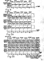
- FIG. 5a a schematic diagram of the assignment of time intervals for system bus access by four of data processing units is shown.
- the system bus is divided into a plurality of sub-buses, an address signal bus, a write data signal bus, and a read data signal bus.
- data processing unit #1 has access 501a to address signal bus
- data processing unit #3 has access 502a to the write data signal bus
- data processing unit #4 has access 503a to the read data signal bus.
- time period t 2 data processing unit #2 has access 501b to the address signal bus
- data processing unit #4 has access 502b to the write data signal bus
- data processing unit #1 has access 503b to read data signal bus.
- data processing unit #3 has access 501c to address signal bus
- data processing unit #1 has access 502c to write data signal bus
- data processing unit #2 has access 503c to read data signal bus.
- the progression for each succeeding period follows the data processing unit periodic access sequences thus established by these time periods.
- each cache memory unit having a plurality of cache memory sub-units is shown.
- the address signal bus, the write data signal bus and the read data signal bus are coupled to the cache memory units.
- the cache memory sub-units are also indexed in a similar manner.
- each cache memory unit is divided into four cache memory sub-units. The indexing of the system bus access periods occurs sequentially for each cache memory unit and sequentially for each cache memory sub-unit.
- the cache memory sub-unit #1 of cache memory unit #1 accesses 504a on the address signal bus
- cache memory sub-system #2 of data processing unit #2 accesses 505a
- the write data signal bus and cache memory unit #2 of data processing unit m #2 of data processing unit # accesses 505a
- the write data signal bus and cache memory unit #2 of data processing unit #4 accesses 506a the read signal bus.
- the cache memory sub-unit #2 of data processing unit #2 accesses 504b.
- the address signal bus while cache menmory sub-unit #3 of data processing system #4 accesses 505b the write data bus and cache memory sub-unit #4 of data processing unit #1 accesses 506b, the read data signal bus.
- cache memory sub-unit #3 of data processing system #3 accesses 504c, the address signal bus, while cache memory sub-unit #1 of data processing unit #l accesses 505c the write data signal bus and cache memory unit #1 of data processing unit #2 accesses 506c the read data signal bus.
- cache memory sub-unit #1 of data processing unit #4 accesses 504h the address signal bus, while cache memory sub-unit #3 of data processing unit #2 accesses 505h the write data signal bus and cache memory sub-unit #3 of data processing unit #3 accesses 506h the read data signal bus.
- This procedure illustrates how a cyclic access can proceed in the procedure of periodic access by the cache memory sub-units.
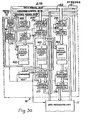
- Main memory control unit 61 is coupled to main memory address signal register 62, data in signal register 63, data out signal register 64, signal combining unit 66 and main memory storage cell array 65.
- Main memory control unit 61 receives control signals from the control signal bus 153 and, based on these signals, executes the manipulation of data signal groups stored in main memory storage cell array 65.
- Address signal register 62 can receive an address signal group from the address signal bus 152 and can apply signals to the main memory storage cell array 65 for activating a group of storage cell storing binary data signal group at a location determined by the address signal group.
- Main memory data in signal register 63 receives signals from the read data signal bus 153a and can apply these signals to main memory storage cell array 65, at a physical location determined by the contents of the address register 62, and to signal combining unit 66.
- Main memory storage cell array 65 can apply signals at an address determined by the contents of address register 62 to signal combining unit 66.
- the contents of switch 66 are applied to data out signal register 64 and to the write data signal bus 153b.
- Control signal input register 168a through control signal input register 168d store signals received from control signal bus 153.
- the control signal bus 153 is coupled to the control signal input registers through a control signal input selector of switch 191.
- an address signal input register 167a through address signal input register 167d associated with each cache memory sub-unit is an address signal input register 167a through address signal input register 167d.
- the address signals are received from address signal bus 152 transferred through address signal input selector or switch 192.
- the data signal bus is coupled to data signal input register 166a through data signal input reigster 166d through data signal input selector or switch 193.
- Control signal input switch 191, address signal input switch 192 and data signal input switch 193 are controlled by cache memory control unit 161 that determines, by the defined system bus access sequence to which cache memory sub-unit the signals applied to the switched are directed.
- the output register control signal output register 178a through control signal output register 178d are coupled to control signal output selector or switch 194. Under control of the cache memory control unit 161, the control signals, if any, are applied to the control signal bus during an appropriate time interval.
- the address signal output register 177a through address signal output register 177d are coupled through address signal output selector or switch 195 to the address signal bus.
- Data signal output selctor or switch 196 controls the distribution of data signals from data signal output register 176a through data signal output reigster 176d to the data signal bus 151.
- the control signal output switch 194, the address signal output switch 195 and data signal output switch are controlled by cache memory control unit 161.
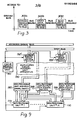
- system bus 15 is coupled to a main memory unit 19 and to a plurality of cache memory units 16 through 17.
- Each cache memory unit is coupled to at least one data processing unit.
- cache memory unit 16 is shown coupled to data processing unit lla, and to data processing unit llb.
- cache memory unit 17 is coupled to data processing unit 13a, data processing unit 13b and data processing unit 13c.
- Data processing unit address signal selector or switch 197 receives address signals from data processing unit 11 (lla) through data processing unit (llc), and applies the address signals to address signal input selector or switch 192'.
- Data processing unit output data selector or switch 198 receives data signals from data processing unit #1 (lla) through data processing unit (llc) and applies the data signals to data signal input selector or switch 193'.
- Data processing unit input data signal selector or switch 199 receives data signals from the cache memory data signal group memory unit and applies these data signals to data processing unit #l (lla) through data processing unit #n (llc). Data processing unit #l through data processing unit #n, data procedssing unit address signal switch 197, data processing unit out data signal switch 198 and data processing unit input data signal switch 199, address signal input switch 192' and data signal input switch 193'.
- the present invention provides an apparatus and method for a greatly enhanced transfer of data signal groups over the system bus.
- the increased performance of the system insures that, the availability of data signal groups from the main memory does not provide a limitation on the system performance.
- the system bus by means of the present invention, has become sufficiently efficient with respect to the transfer of information that the bus was shown to be unused for unacceptable periods of time. It was therefore found possible to vary the structure of the data processing system from one where a cache memory unit was associated with each data processing unit to a structure where a cache memory unit was able to provide temporary storage of data signal groups for a plurality of data processing systems.
- the system bus is coupled, in addition to the main memory, to a plurality of cache memory units, and each of the cache memory units, in turn, can be coupled to a plurality of data processing units.
- the cache memory unit is a signal storage unit for storing signal groups that have been requested by the data processing unit or have a relatively high probability of being requested by the data processing unit, e.g. in the two paths of a decision tree.
- the availability of signal groups is also enhanced by use of transfer of multiple data signal group during a signal operaiton, i.e. programs are typically written with successive instructions in successive storage locations. These data signal groups are more readily available to the associated data processing unit than are the data signal groups stored in the main memory.
- the cache memory unit can be of the type generally referred to as a "write-back" or "write-thru" cache memory unit.
- This type of cache memory unit is distinguished by the mode of operation in which the result of every associated data processing unit operation is returned to the cache memory unit.
- the cache memory unit illustrated in Figure 2a, and Figure 2b has another feature common to cache memory units.
- the address is divided into three parts.
- the first part (labelled x in Figure 2b) defines a physical location in the memory components of the cache memory unit.
- the least significant signal bits are typically omitted when the data bus can transfer a plurality of basic data signal groups.
- the data signal groups are comprised of signal groups usually referred to as words and the data signal groups are always transferred in groups of two words, the final data bit can be omitted in the address (for purposes relevant to the instant invention).
- the final two address signal bits can be omitted.
- the operation of the cache memory unit is thus complicated by the use of the two sub-groups of the address signal group. To determine if a data signal group is stored in the cache memory units, it is first necessary to determine if the associated address signal group is stored in the cache memory unit. An address signal group is therefore entered in address signal input register 167.
- the x-portion of the address signal group is applied to the addressing mechanism of y-address signal group memory unit 163.
- the contents of the location of y-address group memory unit 163 are applied to comparator 165 along with the y-address portion of the address signal group in address signal input reigster 167. If the two y-address signals groups are identical, then the associated data signal group is stored in data signal group memory unit 164.
- the apparatus of cache memory unit 16 is adopted so that when the data signal group is not stored in the cache memory unit, then by means of the cache memory control unit of the address signals are applied to the address signal bus, at the appropriate time, through the selector or switch apparatus.
- this operation is the operation in which a data signal group requested by a data processing unit must first be modified by a data signal group from the requesting data processing unit.
- the data signal group transferred over the system bus can be comprised of a plurality of sub-data signal groups, e.g. words.
- the data processing unit can be arranged to manipulate the data signal sub-groups and can wish to store a resulting data signal sub-group in a memory location not currently stored in the cache memory system.
- the data signal sub-group must then be sent to the main memory, replace the data signal sub-group in a data signal group of the main memory and place the resulting data signal group on the system bus for storage in the cache memory unit.
- the main memory unit 19 of Figure 6 is arranged to expedite the process by combining the input data signal group with the data signal group of the main memory unit address in the signal combining unit 66 without first storing the input data signal group in the main memory. With this apparatus available in the main memory, "the modify" main memory address operation is expedited.
- the most complex system bus access can be decomposed in an address operation, a write (to main memory unit) operation and a read (from the main memory unit) operation.
- each operation is provided with dedicated system sub-buses to perform the data transfer of the operation.
- each sub-operation of an operation can be separated from the other sub-operations as shown in Figure 3 and Figure 5a.
- the access to the system bus can be multiplexed, i.e. each data processing unit having a defined periodic access to the system bus as shown in Figure 4. It has been found that further efficiencies in data signal group transfer can be accomplished by dividing the cache memory unit into a plurality of cache memory sub-units, each cache memory sub-unit for storing data signal groups related to a predefined portion of access signal group space. In the preferred embodiment, the cache memory unit is divided into four cache memory sub-units. Each cache memory sub-unit is identified with an address bit, providing a further simplification with respect to addressing. A further advantage of the use of the plurality of cache memory sub-units can be increased availability of the cache memory unit when a plurality of data processing units are coupled thereto.
- Timing signals defining time intervals for each cache memory unit can be transferred to the cache memory control unit by the control signal bus.
- the techniques for improving the system bus utilization provided the result that, instead of each data processing unit having a cache memory unit associated therewith, the cache memory unit can have a plurality of data processing units associated therewith. This structure provides increased data processing system efficiency.
- a switching mechanism shown symbolically in Figure 7 and Figure 9 must be provided to direct signal groups to the appropriate destination.
- a signal group can be applied to a plurality of input registers, but an appropriate strobe signal will store (or latch) the signal group only in the appropriate register.
- the timing of the application of a signal group to an output reigster can determine the destination.
- the switching or data-directing procedures can be a matter of design choice.
- a bus arbiter can be used to control access to the system bus.
- the bus artiber will maintain the same constraints as the dedicated access procedure, e.g. a cache memory unit cannot access the system bus (even different portions of the system bus) during a single time interval.
- the bus arbiter can provide additional refinements, such as priority procedures, at the expense of increased logic and communication apparatus.
- the bus arbiter can be a portion of the cache memory control unit or can be a separate apparatus supplying signals to said cache memory control unit.
Landscapes
- Engineering & Computer Science (AREA)
- Theoretical Computer Science (AREA)
- Physics & Mathematics (AREA)
- General Engineering & Computer Science (AREA)
- General Physics & Mathematics (AREA)
- Memory System Of A Hierarchy Structure (AREA)
- Multi Processors (AREA)
- Information Transfer Systems (AREA)
Applications Claiming Priority (2)
| Application Number | Priority Date | Filing Date | Title |
|---|---|---|---|
| US06/698,399 US4941088A (en) | 1985-02-05 | 1985-02-05 | Split bus multiprocessing system with data transfer between main memory and caches using interleaving of sub-operations on sub-busses |
| US698399 | 1991-05-10 |
Publications (2)
| Publication Number | Publication Date |
|---|---|
| EP0192366A2 true EP0192366A2 (fr) | 1986-08-27 |
| EP0192366A3 EP0192366A3 (fr) | 1988-10-05 |
Family
ID=24805076
Family Applications (1)
| Application Number | Title | Priority Date | Filing Date |
|---|---|---|---|
| EP86300658A Withdrawn EP0192366A3 (fr) | 1985-02-05 | 1986-01-31 | Appareil et procédé d'amélioration de performances de système-bus dans un système de traitement de données |
Country Status (4)
| Country | Link |
|---|---|
| US (1) | US4941088A (fr) |
| EP (1) | EP0192366A3 (fr) |
| JP (1) | JPS61233858A (fr) |
| AU (1) | AU5297386A (fr) |
Cited By (5)
| Publication number | Priority date | Publication date | Assignee | Title |
|---|---|---|---|---|
| FR2632096A1 (fr) * | 1988-05-26 | 1989-12-01 | Ibm | Systeme de microcalculateur a bus multiple avec arbitrage d'acces aux bus |
| EP0448743A1 (fr) * | 1990-03-26 | 1991-10-02 | Siemens Nixdorf Informationssysteme Aktiengesellschaft | Système multiprocesseur avec un bus pour le couplage de plusieurs unités de traitement avec leurs antémémoires privées et d'une mémoire de travail commune |
| EP0397302A3 (fr) * | 1989-05-12 | 1991-12-04 | Flavors Technology, Inc., | Bus synchrone |
| GB2214670B (en) * | 1988-01-21 | 1992-07-15 | Mitsubishi Electric Corp | Cache system |
| US5289585A (en) * | 1990-03-26 | 1994-02-22 | Siemens Nixdorf Informationssysteme Ag | Multiprocessor system having a system bus for the coupling of several processing units with appertaining private cache memories and a common main memory |
Families Citing this family (12)
| Publication number | Priority date | Publication date | Assignee | Title |
|---|---|---|---|---|
| DE3788721T2 (de) * | 1986-10-17 | 1994-06-09 | Fujitsu Ltd | Datenübertragungssystem mit übertragunsdiskriminierungsschaltung. |
| JP3411300B2 (ja) | 1992-02-18 | 2003-05-26 | 株式会社日立製作所 | 情報処理装置 |
| US5581734A (en) * | 1993-08-02 | 1996-12-03 | International Business Machines Corporation | Multiprocessor system with shared cache and data input/output circuitry for transferring data amount greater than system bus capacity |
| US5457795A (en) * | 1994-06-01 | 1995-10-10 | Willman; Todd J. | Method and apparatus for sharing and transferring data between software programs |
| US5826045A (en) * | 1995-12-11 | 1998-10-20 | Ncr Corporation | Arbitration parking apparatus and method for a split transaction bus in a multiprocessor computer system |
| JPH1055674A (ja) * | 1996-08-09 | 1998-02-24 | Nec Corp | 半導体記憶装置 |
| US6560674B1 (en) * | 1998-10-14 | 2003-05-06 | Hitachi, Ltd. | Data cache system |
| JP3457611B2 (ja) * | 2000-02-16 | 2003-10-20 | 日本電気株式会社 | 半導体記憶装置 |
| JP4306997B2 (ja) * | 2000-05-12 | 2009-08-05 | 富士通株式会社 | データ制御装置及びatm制御装置 |
| US20090228612A1 (en) * | 2008-03-06 | 2009-09-10 | Barinder Singh Rai | Flexible Bus Interface and Method for Operating the Same |
| CN102574053A (zh) | 2009-08-04 | 2012-07-11 | 二氧化碳处理公司 | 使用碳酸盐和生物催化剂捕获co2的制剂和方法 |
| WO2020226903A1 (fr) * | 2019-05-07 | 2020-11-12 | MemryX Inc. | Architecture d'unité de traitement de mémoire |
Family Cites Families (11)
| Publication number | Priority date | Publication date | Assignee | Title |
|---|---|---|---|---|
| US4084234A (en) * | 1977-02-17 | 1978-04-11 | Honeywell Information Systems Inc. | Cache write capacity |
| US4141067A (en) * | 1977-06-13 | 1979-02-20 | General Automation | Multiprocessor system with cache memory |
| US4449183A (en) * | 1979-07-09 | 1984-05-15 | Digital Equipment Corporation | Arbitration scheme for a multiported shared functional device for use in multiprocessing systems |
| FR2465281A1 (fr) * | 1979-09-12 | 1981-03-20 | Telediffusion Fse | Dispositif de transmission numerique et d'affichage de graphismes et/ou de caracteres sur un ecran |
| US4392200A (en) * | 1980-01-28 | 1983-07-05 | Digital Equipment Corporation | Cached multiprocessor system with pipeline timing |
| US4323967A (en) * | 1980-04-15 | 1982-04-06 | Honeywell Information Systems Inc. | Local bus interface for controlling information transfers between units in a central subsystem |
| US4425615A (en) * | 1980-11-14 | 1984-01-10 | Sperry Corporation | Hierarchical memory system having cache/disk subsystem with command queues for plural disks |
| US4445172A (en) * | 1980-12-31 | 1984-04-24 | Honeywell Information Systems Inc. | Data steering logic for the output of a cache memory having an odd/even bank structure |
| US4622631B1 (en) * | 1983-12-30 | 1996-04-09 | Recognition Int Inc | Data processing system having a data coherence solution |
| US4695943A (en) * | 1984-09-27 | 1987-09-22 | Honeywell Information Systems Inc. | Multiprocessor shared pipeline cache memory with split cycle and concurrent utilization |
| US4604743A (en) * | 1984-11-21 | 1986-08-05 | North American Philips Corporation | Bus structure for an image processor |
-
1985
- 1985-02-05 US US06/698,399 patent/US4941088A/en not_active Expired - Fee Related
-
1986
- 1986-01-31 EP EP86300658A patent/EP0192366A3/fr not_active Withdrawn
- 1986-02-04 AU AU52973/86A patent/AU5297386A/en not_active Abandoned
- 1986-02-05 JP JP61022198A patent/JPS61233858A/ja active Pending
Cited By (8)
| Publication number | Priority date | Publication date | Assignee | Title |
|---|---|---|---|---|
| GB2214670B (en) * | 1988-01-21 | 1992-07-15 | Mitsubishi Electric Corp | Cache system |
| FR2632096A1 (fr) * | 1988-05-26 | 1989-12-01 | Ibm | Systeme de microcalculateur a bus multiple avec arbitrage d'acces aux bus |
| EP0343770A3 (en) * | 1988-05-26 | 1990-11-22 | International Business Machines Corporation | Multi-bus microcomputer system with bus arbitration |
| BE1002405A4 (fr) * | 1988-05-26 | 1991-01-29 | Ibm | Systeme de microcalculateur a bus multiple avec arbitrage d'acces aux bus. |
| US5129090A (en) * | 1988-05-26 | 1992-07-07 | Ibm Corporation | System bus preempt for 80386 when running in an 80386/82385 microcomputer system with arbitration |
| EP0397302A3 (fr) * | 1989-05-12 | 1991-12-04 | Flavors Technology, Inc., | Bus synchrone |
| EP0448743A1 (fr) * | 1990-03-26 | 1991-10-02 | Siemens Nixdorf Informationssysteme Aktiengesellschaft | Système multiprocesseur avec un bus pour le couplage de plusieurs unités de traitement avec leurs antémémoires privées et d'une mémoire de travail commune |
| US5289585A (en) * | 1990-03-26 | 1994-02-22 | Siemens Nixdorf Informationssysteme Ag | Multiprocessor system having a system bus for the coupling of several processing units with appertaining private cache memories and a common main memory |
Also Published As
| Publication number | Publication date |
|---|---|
| JPS61233858A (ja) | 1986-10-18 |
| EP0192366A3 (fr) | 1988-10-05 |
| AU5297386A (en) | 1986-08-14 |
| US4941088A (en) | 1990-07-10 |
Similar Documents
| Publication | Publication Date | Title |
|---|---|---|
| EP0192366A2 (fr) | Appareil et procédé d'amélioration de performances de système-bus dans un système de traitement de données | |
| US5434970A (en) | System for distributed multiprocessor communication | |
| EP1345125B1 (fr) | Système DRAM avec dispositif de prévention de conflit de bancs | |
| US6505287B2 (en) | Virtual channel memory access controlling circuit | |
| US5752256A (en) | Disk array apparatus and method for dividing and reading/writing partial data across a plurality of drive groups utilizing parallel processing | |
| US7660951B2 (en) | Atomic read/write support in a multi-module memory configuration | |
| US3931613A (en) | Data processing system | |
| US5898882A (en) | Method and system for enhanced instruction dispatch in a superscalar processor system utilizing independently accessed intermediate storage | |
| JPH04348451A (ja) | 並列計算機 | |
| RU2042193C1 (ru) | Вычислительная система | |
| US5526487A (en) | System for multiprocessor communication | |
| US6034965A (en) | Multi-stream associative memory architecture for computer telephony | |
| JPH08235143A (ja) | クラスタ構成の並列計算機 | |
| EP0081358B1 (fr) | Système de traitement de données fournissant un transfert de données entre modules | |
| JPH03189843A (ja) | データ処理システムおよび方法 | |
| US5923891A (en) | System for minimizing disk access using the computer maximum seek time between two furthest apart addresses to control the wait period of the processing element | |
| US5506980A (en) | Method and apparatus for parallel processing of a large data array utilizing a shared auxiliary memory | |
| JP2598441B2 (ja) | ベクトルデータ処理装置 | |
| RU2263951C2 (ru) | Способ обработки цифровых данных в запоминающем устройстве и запоминающее устройство для осуществления способа | |
| US6944698B2 (en) | Method and apparatus for providing bus arbitrations in a data processing system | |
| Chaudhry et al. | Cache interleaving in multiprocessor systems | |
| JPS61118847A (ja) | メモリの同時アクセス制御方式 | |
| JP2540844B2 (ja) | デ−タ転送制御方法 | |
| JPH0525341B2 (fr) | ||
| JPS60169946A (ja) | タスク制御方式 |
Legal Events
| Date | Code | Title | Description |
|---|---|---|---|
| PUAI | Public reference made under article 153(3) epc to a published international application that has entered the european phase |
Free format text: ORIGINAL CODE: 0009012 |
|
| AK | Designated contracting states |
Kind code of ref document: A2 Designated state(s): AT BE CH DE FR GB IT LI LU NL SE |
|
| PUAL | Search report despatched |
Free format text: ORIGINAL CODE: 0009013 |
|
| AK | Designated contracting states |
Kind code of ref document: A3 Designated state(s): AT BE CH DE FR GB IT LI LU NL SE |
|
| STAA | Information on the status of an ep patent application or granted ep patent |
Free format text: STATUS: THE APPLICATION IS DEEMED TO BE WITHDRAWN |
|
| 18D | Application deemed to be withdrawn |
Effective date: 19890406 |
|
| RIN1 | Information on inventor provided before grant (corrected) |
Inventor name: SHAFFER, STEPHEN JAY Inventor name: STRECKER, WILLIAM D. Inventor name: WARREN, RICHARD ALAN Inventor name: EGGERS, THOMAS W. |