EP0193117A2 - Procédé pour la fabrication d'un dispositif semi-conducteur - Google Patents
Procédé pour la fabrication d'un dispositif semi-conducteur Download PDFInfo
- Publication number
- EP0193117A2 EP0193117A2 EP86102226A EP86102226A EP0193117A2 EP 0193117 A2 EP0193117 A2 EP 0193117A2 EP 86102226 A EP86102226 A EP 86102226A EP 86102226 A EP86102226 A EP 86102226A EP 0193117 A2 EP0193117 A2 EP 0193117A2
- Authority
- EP
- European Patent Office
- Prior art keywords
- silicon layer
- ion
- polycrystalline silicon
- layer
- amorphous silicon
- Prior art date
- Legal status (The legal status is an assumption and is not a legal conclusion. Google has not performed a legal analysis and makes no representation as to the accuracy of the status listed.)
- Granted
Links
Images

Classifications
-
- H—ELECTRICITY
- H10—SEMICONDUCTOR DEVICES; ELECTRIC SOLID-STATE DEVICES NOT OTHERWISE PROVIDED FOR
- H10D—INORGANIC ELECTRIC SEMICONDUCTOR DEVICES
- H10D30/00—Field-effect transistors [FET]
- H10D30/01—Manufacture or treatment
- H10D30/021—Manufacture or treatment of FETs having insulated gates [IGFET]
- H10D30/0223—Manufacture or treatment of FETs having insulated gates [IGFET] having source and drain regions or source and drain extensions self-aligned to sides of the gate
- H10D30/0227—Manufacture or treatment of FETs having insulated gates [IGFET] having source and drain regions or source and drain extensions self-aligned to sides of the gate having both lightly-doped source and drain extensions and source and drain regions self-aligned to the sides of the gate, e.g. lightly-doped drain [LDD] MOSFET or double-diffused drain [DDD] MOSFET
-
- H—ELECTRICITY
- H10—SEMICONDUCTOR DEVICES; ELECTRIC SOLID-STATE DEVICES NOT OTHERWISE PROVIDED FOR
- H10D—INORGANIC ELECTRIC SEMICONDUCTOR DEVICES
- H10D30/00—Field-effect transistors [FET]
- H10D30/60—Insulated-gate field-effect transistors [IGFET]
-
- H—ELECTRICITY
- H10—SEMICONDUCTOR DEVICES; ELECTRIC SOLID-STATE DEVICES NOT OTHERWISE PROVIDED FOR
- H10D—INORGANIC ELECTRIC SEMICONDUCTOR DEVICES
- H10D62/00—Semiconductor bodies, or regions thereof, of devices having potential barriers
- H10D62/10—Shapes, relative sizes or dispositions of the regions of the semiconductor bodies; Shapes of the semiconductor bodies
- H10D62/17—Semiconductor regions connected to electrodes not carrying current to be rectified, amplified or switched, e.g. channel regions
- H10D62/351—Substrate regions of field-effect devices
- H10D62/357—Substrate regions of field-effect devices of FETs
- H10D62/364—Substrate regions of field-effect devices of FETs of IGFETs
- H10D62/371—Inactive supplementary semiconductor regions, e.g. for preventing punch-through, improving capacity effect or leakage current
-
- H—ELECTRICITY
- H10—SEMICONDUCTOR DEVICES; ELECTRIC SOLID-STATE DEVICES NOT OTHERWISE PROVIDED FOR
- H10P—GENERIC PROCESSES OR APPARATUS FOR THE MANUFACTURE OR TREATMENT OF DEVICES COVERED BY CLASS H10
- H10P32/00—Diffusion of dopants within, into or out of wafers, substrates or parts of devices
- H10P32/30—Diffusion for doping of conductive or resistive layers
- H10P32/302—Doping polycrystalline silicon or amorphous silicon layers
-
- H—ELECTRICITY
- H10—SEMICONDUCTOR DEVICES; ELECTRIC SOLID-STATE DEVICES NOT OTHERWISE PROVIDED FOR
- H10P—GENERIC PROCESSES OR APPARATUS FOR THE MANUFACTURE OR TREATMENT OF DEVICES COVERED BY CLASS H10
- H10P76/00—Manufacture or treatment of masks on semiconductor bodies, e.g. by lithography or photolithography
- H10P76/40—Manufacture or treatment of masks on semiconductor bodies, e.g. by lithography or photolithography of masks comprising inorganic materials
- H10P76/403—Manufacture or treatment of masks on semiconductor bodies, e.g. by lithography or photolithography of masks comprising inorganic materials for lift-off processes
-
- H—ELECTRICITY
- H10—SEMICONDUCTOR DEVICES; ELECTRIC SOLID-STATE DEVICES NOT OTHERWISE PROVIDED FOR
- H10P—GENERIC PROCESSES OR APPARATUS FOR THE MANUFACTURE OR TREATMENT OF DEVICES COVERED BY CLASS H10
- H10P76/00—Manufacture or treatment of masks on semiconductor bodies, e.g. by lithography or photolithography
- H10P76/40—Manufacture or treatment of masks on semiconductor bodies, e.g. by lithography or photolithography of masks comprising inorganic materials
- H10P76/408—Manufacture or treatment of masks on semiconductor bodies, e.g. by lithography or photolithography of masks comprising inorganic materials characterised by their sizes, orientations, dispositions, behaviours or shapes
- H10P76/4085—Manufacture or treatment of masks on semiconductor bodies, e.g. by lithography or photolithography of masks comprising inorganic materials characterised by their sizes, orientations, dispositions, behaviours or shapes characterised by the processes involved to create the masks
-
- Y—GENERAL TAGGING OF NEW TECHNOLOGICAL DEVELOPMENTS; GENERAL TAGGING OF CROSS-SECTIONAL TECHNOLOGIES SPANNING OVER SEVERAL SECTIONS OF THE IPC; TECHNICAL SUBJECTS COVERED BY FORMER USPC CROSS-REFERENCE ART COLLECTIONS [XRACs] AND DIGESTS
- Y10—TECHNICAL SUBJECTS COVERED BY FORMER USPC
- Y10S—TECHNICAL SUBJECTS COVERED BY FORMER USPC CROSS-REFERENCE ART COLLECTIONS [XRACs] AND DIGESTS
- Y10S148/00—Metal treatment
- Y10S148/061—Gettering-armorphous layers
-
- Y—GENERAL TAGGING OF NEW TECHNOLOGICAL DEVELOPMENTS; GENERAL TAGGING OF CROSS-SECTIONAL TECHNOLOGIES SPANNING OVER SEVERAL SECTIONS OF THE IPC; TECHNICAL SUBJECTS COVERED BY FORMER USPC CROSS-REFERENCE ART COLLECTIONS [XRACs] AND DIGESTS
- Y10—TECHNICAL SUBJECTS COVERED BY FORMER USPC
- Y10S—TECHNICAL SUBJECTS COVERED BY FORMER USPC CROSS-REFERENCE ART COLLECTIONS [XRACs] AND DIGESTS
- Y10S148/00—Metal treatment
- Y10S148/082—Ion implantation FETs/COMs
Definitions
- the present invention relates to a method of manufacturing a semiconductor device, and more particularly, to a method of manufacturing an MOS type transistor.
- Element isolation region 2 is formed on the surface of p-type semiconductor substrate 1.
- Gate electrode 4 of polycrystalline silicon, is then formed on substrate 1 through gate oxide film 3.
- Shallow n -type regions 5a and 5b are formed by ion-implanting arsenic in substrate 1, using gate electrode 4 as a mask. Boron is then ion-implanted in substrate 1 at an acceleration voltage of 80 kV and a dose of 3 x 10 12 /cm 2 to form p + -type regions 6a and 6b (Fig. lA).
- CVD-Si0 2 layer 7 is deposited over the entire surface of the resultant structure. Layer 7 is then removed using reactive ion etching (RIE) so that it remains on only the side walls of gate electrode 4 and gate oxide film 3.
- RIE reactive ion etching
- N +- type regions 8a and 8b are then formed by ion-implanting phosphorus in substrate 1, using remaining S i 02 layer 7 and gate electrode 4 as masks.
- Source region 9 consists of regions 5a and 8a
- drain region 10 consists of regions 5b and 8b.
- P +- type regions, so-called p-pocket regions lla and llb, are then formed beneath regions 5a and 5b.
- Protective film 12 is formed over the entire resultant structure.
- Contact holes 13 are then formed by selectively removing portions of protective film 12 corresponding to regions 8a and 8b. Finally, At electrodes 14 are formed in contact holes 13, thus forming an MOS transistor having an LDD (lightly-doped drain) structure (Fig. lB).
- LDD lightly-doped drain
- a method of manufacturing a semiconductor device comprising the steps of forming an insulating film on a semiconductor substrate, forming a polycrystalline silicon layer on the insulating film, converting either all of the polycrystalline silicon layer or a portion of the polycrystalline silicon layer, whose thickness is predetermined, into an amorphous silicon layer, patterning the polycrystalline silicon layer, either all of which or a portion of which, whose thickness is predetermined, has been converted into an amorphous silicon layer, and ion-implanting an impurity in the semiconductor substrate using the patterned layer as a mask.
- the method of the present invention it is possible to convert a polycrystalline silicon layer into an amorphous silicon layer by ion-implanting an impurity in the polycrystalline silicon layer.
- an impurity an atom which has a large atomic radius and which can therefore easily convert polycrystalline silicon to amorphous silicon is preferable.
- An n-type impurity is preferable, because with p-type ions, the resistance of amorphous silicon increases undesirably.
- Preferable atoms are silicon, fluorine, phosphorus, arsenic, and argon atoms.
- the acceleration voltage and ion dose for ion implantation need only be sufficient to convert at least a portion of the polycrstalline silicon layer, whose thickness is perdetermined, to an amorphous silicon layer.
- the method of the present invention can be applied not only to the manufacture of a MOS transistor, but also to the formation of an electrode of a capacitor formed together on a single substrate with a device requiring ion implantation. Impurity penetration can, in this application, be prevented in the same manner as described above.
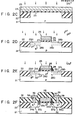
- Element isolation region 22 was first formed on the surface of p-type (100) silicon substrate 21 (outside the element region thereof) by selective oxidation (Fig. 2A).
- Oxide film 23 having a thickness of 250 A was then formed on the entire surface of substrate 21 0 in an oxygen atmosphere.
- Undoped, 4,000 A thick polysilicon layer 24 was formed.
- Phosphorus was then diffused into layer 24 using the pOCl 3 diffusion method (Fig. 2B), and silicon was ion-implanted into the entire surface of layer 24 at an acceleration voltage of 180 kV and a dose of 2 x 10 15 /cm 2 .
- the region ⁇ from the surface of layer 24 to a depth of about 2,500 A thereof was converted to amorphous silicon layer 25 (Fig.
- Layer 25, layer 24, and oxide film 23 were then properly etched using photolithography, RIE, or a similar method, and gate electrode 26 and gate oxide film 27 were formed.
- Boron-doped layers 28a and 28b were formed by ion-implanting boron (for p-pocket formation) in substrate 21 at an acceleration voltage of 80 kV and a dose of 3 x 10 12 /cm 2 .
- Phosphorus-doped layers 29a and 29b were then formed by ion-implanting phosphorus (for n - -type region formation) at an acceleration voltage of 35 k V and a dose of 2 x 10 13 / cm 2 .
- CVD-SiO 2 film 30 was deposited to a thick- ness of 3,000 A over the entire surface of the resultant structure. Etching was performed using an RIE technique, so that portions of Si0 2 film 30 were left on only the side walls of gate electrode 26 and gate oxide film 27.
- Arsenic-doped layers 31a and 31b were then formed by ion-implanting arsenic (for the formation of an n +- type region) at an acceleration voltage of 40 kV and a dose of 5 x 10 15 /cm 2 , using film 30 and electrode 26 as a mask (Fig. 2E).
- PSG (phosphosilicate glass) 0 film 32 was deposited to a thickness of 5,000 A over the entire surface of the structure as a protective film.
- Annealing was then performed in a nitrogen atmosphere at a temperature of 900°C for 20 minutes in order to electrically activate the ion-implanted impurities. This resulted in the formation of source region 35, consisting of regions 33a and region 34a; drain region 36, consisting of regions 33b and 34b, and p-pockets 37a and 37b. At the same time, the upper portion of the amorphous silicon layer of gate electrode 26 was converted into a polycrystalline silicon layer. The surface resistance of gate electrode 26 did not increase. Contact holes 38 were then formed by selectively removing portions of PSG film 32 corresponding to regions 34a and 34b. Aluminum was deposited to a thickness of about 1.0 pm over the entire surface, and patterned to obtain At electrode 39, resulting in an n-channel MOS transistor having an LDD/p-pocket structure (Fig. 2F).
- undoped polycrystalline silicon layer 24 was formed on silicon substrate 21 through oxide film 23. Phosphorus was then diffused in substrate 21 using a POCl 3 technique, and amorphous silicon layer 25 was formed by ion-implanting silicon in the upper portion of layer 24.
- amorphous silicon layer 25 was formed by ion-implanting silicon in the upper portion of layer 24.
- the penetration of boron ions through gate electrode 26 and gate oxide film 27 into substrate 21 during the ion implantation of boron (for p-pocket formation) can be prevented.
- the boron ions are stopped at the polycrystalline silicon layer or the amorphous silicon layer of gate electrode 26, thus preventing the channeling phenomenon and guaranteeing a constant threshold voltage.
- phosphorus was used as an impurity to convert a polycrystalline silicon layer into an n-conductivity type layer, but boron or the like can also be used to convert the layer into a p-conductivity type layer.
- the present invention was applied to the manufacture of an n-channel MOS transistor having an LDD/p-pocket structure.
- the present invention is not limited to this. It is equally effective in the prevention of ion penetration through the gate electrode and the like during ion implantation of boron for forming p-channel source and drain regions in a CMOS IC, in which n- and p-channel transistors are formed together on the same substrate.
Landscapes
- Insulated Gate Type Field-Effect Transistor (AREA)
- Metal-Oxide And Bipolar Metal-Oxide Semiconductor Integrated Circuits (AREA)
Applications Claiming Priority (2)
| Application Number | Priority Date | Filing Date | Title |
|---|---|---|---|
| JP30508/85 | 1985-02-20 | ||
| JP60030508A JPS61191070A (ja) | 1985-02-20 | 1985-02-20 | 半導体装置の製造方法 |
Publications (3)
| Publication Number | Publication Date |
|---|---|
| EP0193117A2 true EP0193117A2 (fr) | 1986-09-03 |
| EP0193117A3 EP0193117A3 (en) | 1989-05-31 |
| EP0193117B1 EP0193117B1 (fr) | 1992-07-15 |
Family
ID=12305752
Family Applications (1)
| Application Number | Title | Priority Date | Filing Date |
|---|---|---|---|
| EP86102226A Expired - Lifetime EP0193117B1 (fr) | 1985-02-20 | 1986-02-20 | Procédé pour la fabrication d'un dispositif semi-conducteur |
Country Status (4)
| Country | Link |
|---|---|
| US (1) | US4697333A (fr) |
| EP (1) | EP0193117B1 (fr) |
| JP (1) | JPS61191070A (fr) |
| DE (1) | DE3685970T2 (fr) |
Cited By (9)
| Publication number | Priority date | Publication date | Assignee | Title |
|---|---|---|---|---|
| GB2167899A (en) * | 1984-11-15 | 1986-06-04 | Sony Corp | Method of manufacturing thin film transistors |
| EP0465045A3 (en) * | 1990-06-26 | 1992-05-20 | American Telephone And Telegraph Company | Method of field effect transistor fabrication for integrated circuits |
| EP0507567A3 (en) * | 1991-04-01 | 1993-04-21 | Sgs-Thomson Microelectronics, Inc. | Field effect transistor structure and method of fabrication |
| EP0588032A3 (en) * | 1992-08-19 | 1996-01-31 | St Microelectronics Srl | Process for forming implanted regions with lowered channeling risk on semiconductors |
| EP0717448A1 (fr) * | 1994-12-16 | 1996-06-19 | Sun Microsystems, Inc. | Dispositif MOS à faible puissance asymétrique |
| EP0534530A3 (en) * | 1991-09-23 | 1996-08-28 | Koninkl Philips Electronics Nv | Method of manufacturing a device whereby a substance is implanted into a body |
| EP0774785A3 (fr) * | 1995-11-20 | 1997-07-16 | At & T Corp | Dispositifs de protection électrostatique pour protéger un circuit intégré semi-conducteur |
| US5650340A (en) * | 1994-08-18 | 1997-07-22 | Sun Microsystems, Inc. | Method of making asymmetric low power MOS devices |
| WO2004107450A1 (fr) * | 2003-05-30 | 2004-12-09 | Fujitsu Limited | Semi-conducteur et son procede de fabrication |
Families Citing this family (52)
| Publication number | Priority date | Publication date | Assignee | Title |
|---|---|---|---|---|
| JPH0616556B2 (ja) * | 1987-04-14 | 1994-03-02 | 株式会社東芝 | 半導体装置 |
| US4851746A (en) * | 1987-04-15 | 1989-07-25 | Republic Industries, Inc. | Sensing apparatus for automatic door |
| AU599223B2 (en) * | 1987-04-15 | 1990-07-12 | Semiconductor Energy Laboratory Co. Ltd. | Superconducting ceramic pattern and its manufacturing method |
| US4818711A (en) * | 1987-08-28 | 1989-04-04 | Intel Corporation | High quality oxide on an ion implanted polysilicon surface |
| US5017509A (en) * | 1988-07-19 | 1991-05-21 | Regents Of The University Of California | Stand-off transmission lines and method for making same |
| JPH0770727B2 (ja) * | 1989-06-16 | 1995-07-31 | 日本電装株式会社 | Misトランジスタ及び相補形misトランジスタの製造方法 |
| US5170232A (en) * | 1989-08-24 | 1992-12-08 | Nec Corporation | MOS field-effect transistor with sidewall spacers |
| US5043292A (en) * | 1990-05-31 | 1991-08-27 | National Semiconductor Corporation | Self-aligned masking for ultra-high energy implants with application to localized buried implants and insolation structures |
| JPH04241466A (ja) * | 1991-01-16 | 1992-08-28 | Casio Comput Co Ltd | 電界効果型トランジスタ |
| US5187117A (en) * | 1991-03-04 | 1993-02-16 | Ixys Corporation | Single diffusion process for fabricating semiconductor devices |
| JPH05198795A (ja) * | 1991-08-21 | 1993-08-06 | Ricoh Co Ltd | MIS型半導体素子用PolySiゲート電極 |
| US5418398A (en) * | 1992-05-29 | 1995-05-23 | Sgs-Thomson Microelectronics, Inc. | Conductive structures in integrated circuits |
| US5563093A (en) * | 1993-01-28 | 1996-10-08 | Kawasaki Steel Corporation | Method of manufacturing fet semiconductor devices with polysilicon gate having large grain sizes |
| US5350698A (en) * | 1993-05-03 | 1994-09-27 | United Microelectronics Corporation | Multilayer polysilicon gate self-align process for VLSI CMOS device |
| US5371396A (en) * | 1993-07-02 | 1994-12-06 | Thunderbird Technologies, Inc. | Field effect transistor having polycrystalline silicon gate junction |
| US6498080B1 (en) * | 1993-11-05 | 2002-12-24 | Agere Systems Guardian Corp. | Transistor fabrication method |
| US5451532A (en) * | 1994-03-15 | 1995-09-19 | National Semiconductor Corp. | Process for making self-aligned polysilicon base contact in a bipolar junction transistor |
| US5397722A (en) * | 1994-03-15 | 1995-03-14 | National Semiconductor Corporation | Process for making self-aligned source/drain polysilicon or polysilicide contacts in field effect transistors |
| US5641708A (en) * | 1994-06-07 | 1997-06-24 | Sgs-Thomson Microelectronics, Inc. | Method for fabricating conductive structures in integrated circuits |
| US5773309A (en) * | 1994-10-14 | 1998-06-30 | The Regents Of The University Of California | Method for producing silicon thin-film transistors with enhanced forward current drive |
| US5516711A (en) * | 1994-12-16 | 1996-05-14 | Mosel Vitelic, Inc. | Method for forming LDD CMOS with oblique implantation |
| KR970701932A (ko) * | 1995-01-17 | 1997-04-12 | 클라크 3세 존엠. | 고전압 nmos 장치의 개선된 수행을 위한 연장된 드레인 영역에 인과 비소의 공통 주입(co-implantation of arsenic and phosphorus in extended drain region for improved performance of high voltage nmos device) |
| US5652156A (en) * | 1995-04-10 | 1997-07-29 | Taiwan Semiconductor Manufacturing Company Ltd. | Layered polysilicon deposition method |
| US5504024A (en) * | 1995-07-14 | 1996-04-02 | United Microelectronics Corp. | Method for fabricating MOS transistors |
| US6703672B1 (en) * | 1995-09-29 | 2004-03-09 | Intel Corporation | Polysilicon/amorphous silicon composite gate electrode |
| US20020197838A1 (en) * | 1996-01-16 | 2002-12-26 | Sailesh Chittipeddi | Transistor fabrication method |
| US5665611A (en) * | 1996-01-31 | 1997-09-09 | Micron Technology, Inc. | Method of forming a thin film transistor using fluorine passivation |
| US6346439B1 (en) | 1996-07-09 | 2002-02-12 | Micron Technology, Inc. | Semiconductor transistor devices and methods for forming semiconductor transistor devices |
| JP3413823B2 (ja) * | 1996-03-07 | 2003-06-09 | 日本電気株式会社 | 半導体装置及びその製造方法 |
| US5686324A (en) * | 1996-03-28 | 1997-11-11 | Mosel Vitelic, Inc. | Process for forming LDD CMOS using large-tilt-angle ion implantation |
| US5827747A (en) * | 1996-03-28 | 1998-10-27 | Mosel Vitelic, Inc. | Method for forming LDD CMOS using double spacers and large-tilt-angle ion implantation |
| AUPO281896A0 (en) * | 1996-10-04 | 1996-10-31 | Unisearch Limited | Reactive ion etching of silica structures for integrated optics applications |
| JP3022374B2 (ja) * | 1997-02-03 | 2000-03-21 | 日本電気株式会社 | 半導体装置の製造方法 |
| US6017808A (en) * | 1997-10-24 | 2000-01-25 | Lsi Logic Corporation | Nitrogen implanted polysilicon gate for MOSFET gate oxide hardening |
| TW399235B (en) * | 1998-12-04 | 2000-07-21 | United Microelectronics Corp | Selective semi-sphere silicon grain manufacturing method |
| US6069061A (en) * | 1999-02-08 | 2000-05-30 | United Microelectronics Corp. | Method for forming polysilicon gate |
| US6743680B1 (en) | 2000-06-22 | 2004-06-01 | Advanced Micro Devices, Inc. | Process for manufacturing transistors having silicon/germanium channel regions |
| US6461945B1 (en) | 2000-06-22 | 2002-10-08 | Advanced Micro Devices, Inc. | Solid phase epitaxy process for manufacturing transistors having silicon/germanium channel regions |
| US6630386B1 (en) | 2000-07-18 | 2003-10-07 | Advanced Micro Devices, Inc | CMOS manufacturing process with self-amorphized source/drain junctions and extensions |
| US6521502B1 (en) | 2000-08-07 | 2003-02-18 | Advanced Micro Devices, Inc. | Solid phase epitaxy activation process for source/drain junction extensions and halo regions |
| US6472282B1 (en) * | 2000-08-15 | 2002-10-29 | Advanced Micro Devices, Inc. | Self-amorphized regions for transistors |
| US6475869B1 (en) | 2001-02-26 | 2002-11-05 | Advanced Micro Devices, Inc. | Method of forming a double gate transistor having an epitaxial silicon/germanium channel region |
| US20040201067A1 (en) * | 2002-07-08 | 2004-10-14 | Toppoly Optoelectronics Corp. | LLD structure of thin film transistor |
| TW544941B (en) * | 2002-07-08 | 2003-08-01 | Toppoly Optoelectronics Corp | Manufacturing process and structure of thin film transistor |
| US6605514B1 (en) | 2002-07-31 | 2003-08-12 | Advanced Micro Devices, Inc. | Planar finFET patterning using amorphous carbon |
| US20040201068A1 (en) * | 2002-10-02 | 2004-10-14 | Toppoly Optoelectronics Corp. | Process for producing thin film transistor |
| JP4308625B2 (ja) * | 2003-11-07 | 2009-08-05 | パナソニック株式会社 | メモリ混載半導体装置及びその製造方法 |
| JP2007165401A (ja) * | 2005-12-09 | 2007-06-28 | Nec Electronics Corp | 半導体装置および半導体装置の製造方法 |
| WO2008078363A1 (fr) * | 2006-12-22 | 2008-07-03 | Renesas Technology Corp. | Dispositif à semi-conducteurs et son procédé de production |
| KR102223678B1 (ko) * | 2014-07-25 | 2021-03-08 | 삼성디스플레이 주식회사 | 표시장치용 백플레인 및 그 제조 방법 |
| CN105336781A (zh) * | 2014-08-07 | 2016-02-17 | 中芯国际集成电路制造(上海)有限公司 | 源漏结构及其制造方法 |
| CN111129156A (zh) * | 2019-12-27 | 2020-05-08 | 华虹半导体(无锡)有限公司 | Nmos器件的制作方法及以其制作的半导体器件 |
Family Cites Families (9)
| Publication number | Priority date | Publication date | Assignee | Title |
|---|---|---|---|---|
| DE2837800A1 (de) * | 1978-08-30 | 1980-03-13 | Philips Patentverwaltung | Verfahren zum herstellen von halbleiterbauelementen |
| US4442589A (en) * | 1981-03-05 | 1984-04-17 | International Business Machines Corporation | Method for manufacturing field effect transistors |
| US4599118A (en) * | 1981-12-30 | 1986-07-08 | Mostek Corporation | Method of making MOSFET by multiple implantations followed by a diffusion step |
| JPS59920A (ja) * | 1982-06-23 | 1984-01-06 | Fujitsu Ltd | 半導体装置の製造方法 |
| US4472210A (en) * | 1983-01-07 | 1984-09-18 | Rca Corporation | Method of making a semiconductor device to improve conductivity of amorphous silicon films |
| JPS59138379A (ja) * | 1983-01-27 | 1984-08-08 | Toshiba Corp | 半導体装置の製造方法 |
| US4597824A (en) * | 1983-11-11 | 1986-07-01 | Kabushiki Kaisha Toshiba | Method of producing semiconductor device |
| US4555842A (en) * | 1984-03-19 | 1985-12-03 | At&T Bell Laboratories | Method of fabricating VLSI CMOS devices having complementary threshold voltages |
| US4584026A (en) * | 1984-07-25 | 1986-04-22 | Rca Corporation | Ion-implantation of phosphorus, arsenic or boron by pre-amorphizing with fluorine ions |
-
1985
- 1985-02-20 JP JP60030508A patent/JPS61191070A/ja active Granted
-
1986
- 1986-02-19 US US06/830,831 patent/US4697333A/en not_active Expired - Lifetime
- 1986-02-20 EP EP86102226A patent/EP0193117B1/fr not_active Expired - Lifetime
- 1986-02-20 DE DE8686102226T patent/DE3685970T2/de not_active Expired - Fee Related
Cited By (10)
| Publication number | Priority date | Publication date | Assignee | Title |
|---|---|---|---|---|
| GB2167899A (en) * | 1984-11-15 | 1986-06-04 | Sony Corp | Method of manufacturing thin film transistors |
| EP0465045A3 (en) * | 1990-06-26 | 1992-05-20 | American Telephone And Telegraph Company | Method of field effect transistor fabrication for integrated circuits |
| EP0507567A3 (en) * | 1991-04-01 | 1993-04-21 | Sgs-Thomson Microelectronics, Inc. | Field effect transistor structure and method of fabrication |
| EP0534530A3 (en) * | 1991-09-23 | 1996-08-28 | Koninkl Philips Electronics Nv | Method of manufacturing a device whereby a substance is implanted into a body |
| EP0588032A3 (en) * | 1992-08-19 | 1996-01-31 | St Microelectronics Srl | Process for forming implanted regions with lowered channeling risk on semiconductors |
| US5650340A (en) * | 1994-08-18 | 1997-07-22 | Sun Microsystems, Inc. | Method of making asymmetric low power MOS devices |
| US5780912A (en) * | 1994-08-18 | 1998-07-14 | Sun Microsystems, Inc. | Asymmetric low power MOS devices |
| EP0717448A1 (fr) * | 1994-12-16 | 1996-06-19 | Sun Microsystems, Inc. | Dispositif MOS à faible puissance asymétrique |
| EP0774785A3 (fr) * | 1995-11-20 | 1997-07-16 | At & T Corp | Dispositifs de protection électrostatique pour protéger un circuit intégré semi-conducteur |
| WO2004107450A1 (fr) * | 2003-05-30 | 2004-12-09 | Fujitsu Limited | Semi-conducteur et son procede de fabrication |
Also Published As
| Publication number | Publication date |
|---|---|
| JPH0426542B2 (fr) | 1992-05-07 |
| EP0193117A3 (en) | 1989-05-31 |
| JPS61191070A (ja) | 1986-08-25 |
| US4697333A (en) | 1987-10-06 |
| DE3685970D1 (de) | 1992-08-20 |
| EP0193117B1 (fr) | 1992-07-15 |
| DE3685970T2 (de) | 1993-01-14 |
Similar Documents
| Publication | Publication Date | Title |
|---|---|---|
| US4697333A (en) | Method of manufacturing a semiconductor device using amorphous silicon as a mask | |
| US4642878A (en) | Method of making MOS device by sequentially depositing an oxidizable layer and a masking second layer over gated device regions | |
| US5047358A (en) | Process for forming high and low voltage CMOS transistors on a single integrated circuit chip | |
| US5693974A (en) | Elevated source/drain with solid phase diffused source/drain extension for deep sub-micron MOSFETS | |
| US5372957A (en) | Multiple tilted angle ion implantation MOSFET method | |
| US4717683A (en) | CMOS process | |
| EP0258396B1 (fr) | Procede de fabrication de dispositifs mos empiles | |
| KR0130549B1 (ko) | Cmos 장치의 제조방법 | |
| US5472888A (en) | Depletion mode power MOSFET with refractory gate and method of making same | |
| US4891326A (en) | Semiconductor device and a process for manufacturing the same | |
| US5994179A (en) | Method of fabricating a MOSFET featuring an effective suppression of reverse short-channel effect | |
| JPH0628296B2 (ja) | 半導体装置の製造方法 | |
| US5028552A (en) | Method of manufacturing insulated-gate type field effect transistor | |
| US5225357A (en) | Low P+ contact resistance formation by double implant | |
| US5185279A (en) | Method of manufacturing insulated-gate type field effect transistor | |
| EP0187260A2 (fr) | Procédé pour fabriquer un dispositif à circuit intégré semi-conducteur comprenant des MISFETs | |
| KR930005508B1 (ko) | 반도체장치 및 그 제조방법 | |
| US5780347A (en) | Method of forming polysilicon local interconnects | |
| JP3206419B2 (ja) | 半導体装置の製造方法 | |
| JPH098135A (ja) | 半導体装置の製造方法 | |
| JPH05206454A (ja) | Mis型半導体装置の製造方法 | |
| US5869372A (en) | Method of manufacturing a power semiconductor device | |
| JP2968548B2 (ja) | 半導体装置及びその製造方法 | |
| JP2845934B2 (ja) | 半導体集積回路装置の製造方法 | |
| JP2830267B2 (ja) | 半導体装置の製造方法 |
Legal Events
| Date | Code | Title | Description |
|---|---|---|---|
| PUAI | Public reference made under article 153(3) epc to a published international application that has entered the european phase |
Free format text: ORIGINAL CODE: 0009012 |
|
| 17P | Request for examination filed |
Effective date: 19860220 |
|
| AK | Designated contracting states |
Kind code of ref document: A2 Designated state(s): DE FR GB |
|
| PUAL | Search report despatched |
Free format text: ORIGINAL CODE: 0009013 |
|
| AK | Designated contracting states |
Kind code of ref document: A3 Designated state(s): DE FR GB |
|
| RHK1 | Main classification (correction) |
Ipc: H01L 21/31 |
|
| 17Q | First examination report despatched |
Effective date: 19910131 |
|
| GRAA | (expected) grant |
Free format text: ORIGINAL CODE: 0009210 |
|
| AK | Designated contracting states |
Kind code of ref document: B1 Designated state(s): DE FR GB |
|
| REF | Corresponds to: |
Ref document number: 3685970 Country of ref document: DE Date of ref document: 19920820 |
|
| ET | Fr: translation filed | ||
| PLBE | No opposition filed within time limit |
Free format text: ORIGINAL CODE: 0009261 |
|
| STAA | Information on the status of an ep patent application or granted ep patent |
Free format text: STATUS: NO OPPOSITION FILED WITHIN TIME LIMIT |
|
| 26N | No opposition filed | ||
| PGFP | Annual fee paid to national office [announced via postgrant information from national office to epo] |
Ref country code: GB Payment date: 19970211 Year of fee payment: 12 |
|
| PGFP | Annual fee paid to national office [announced via postgrant information from national office to epo] |
Ref country code: DE Payment date: 19970228 Year of fee payment: 12 |
|
| PG25 | Lapsed in a contracting state [announced via postgrant information from national office to epo] |
Ref country code: GB Free format text: LAPSE BECAUSE OF NON-PAYMENT OF DUE FEES Effective date: 19980220 |
|
| GBPC | Gb: european patent ceased through non-payment of renewal fee |
Effective date: 19980220 |
|
| PG25 | Lapsed in a contracting state [announced via postgrant information from national office to epo] |
Ref country code: DE Free format text: LAPSE BECAUSE OF NON-PAYMENT OF DUE FEES Effective date: 19981103 |
|
| REG | Reference to a national code |
Ref country code: FR Ref legal event code: D6 |
|
| PGFP | Annual fee paid to national office [announced via postgrant information from national office to epo] |
Ref country code: FR Payment date: 20050208 Year of fee payment: 20 |