EP0193396A2 - Optisches Signalübertragungssystem mit Pulsfrequenzmodulations-Modem - Google Patents
Optisches Signalübertragungssystem mit Pulsfrequenzmodulations-Modem Download PDFInfo
- Publication number
- EP0193396A2 EP0193396A2 EP86301381A EP86301381A EP0193396A2 EP 0193396 A2 EP0193396 A2 EP 0193396A2 EP 86301381 A EP86301381 A EP 86301381A EP 86301381 A EP86301381 A EP 86301381A EP 0193396 A2 EP0193396 A2 EP 0193396A2
- Authority
- EP
- European Patent Office
- Prior art keywords
- signal
- frequency
- modulated
- pulsed
- pulse
- Prior art date
- Legal status (The legal status is an assumption and is not a legal conclusion. Google has not performed a legal analysis and makes no representation as to the accuracy of the status listed.)
- Granted
Links
Images


Classifications
-
- H—ELECTRICITY
- H04—ELECTRIC COMMUNICATION TECHNIQUE
- H04B—TRANSMISSION
- H04B10/00—Transmission systems employing electromagnetic waves other than radio-waves, e.g. infrared, visible or ultraviolet light, or employing corpuscular radiation, e.g. quantum communication
- H04B10/50—Transmitters
- H04B10/516—Details of coding or modulation
- H04B10/524—Pulse modulation
-
- H—ELECTRICITY
- H04—ELECTRIC COMMUNICATION TECHNIQUE
- H04B—TRANSMISSION
- H04B14/00—Transmission systems not characterised by the medium used for transmission
- H04B14/02—Transmission systems not characterised by the medium used for transmission characterised by the use of pulse modulation
- H04B14/026—Transmission systems not characterised by the medium used for transmission characterised by the use of pulse modulation using pulse time characteristics modulation, e.g. width, position, interval
Definitions
- the present invention generally relates to an optical signal transmission system, and more particularly to an optical signal transmission system employing a novel circuit in a pulsed frequency modulation system.
- a light source In short-haul television transmission for subscribing systems and cable television systems (referred to as "CATVs"), a light source is directly intensity-modulated in response to an input signal in order to easily transmit analog information such as an image (picture) or speech through an optical signal transmission line such as optical fiber cables.
- analog information such as an image (picture) or speech
- optical signal transmission line such as optical fiber cables.
- modulation distortion occurs due to poor linearity of the light source itself, resulting in a degradation of transmission quality.
- An analog signal is pre"modulated by an electronic circuit into a pulse signal. Light from the light source is then intensity-modulated in response to this pulse modulated signal.
- Such modulation systems have been proposed in the form of PWM (pulse width modulation system), PDM (pulse duration modulation system), PFM (pulse frequency modulation system) and pulsed frequency modulation system.
- PWM pulse width modulation system
- PDM pulse duration modulation system
- PFM pulse frequency modulation system
- pulsed FM system is preferred for increasing utilization efficiency of the transmission frequency band.
- This system has many advantages in that multiple transmission can be easily performed, S/N (signal-to-noise) ratio is improved, and offset DC components can be eliminated by AC coupling means in the reception side.
- the FM- modulated analog signal is processed in a predetermined way to obtain a pulsed FM signal.
- This pulsed FM system differs from the PFM (pulse frequency modulation system) in that pulse width as well as pulse frequency are changed in response to the level of the analog signal to be transmitted.
- PFM pulse frequency modulation system
- a modulator capable of a large frequency shift must be employed in order to obtain a pulsed FM signal, it is conventionally difficult to easily produce such a modulator.
- a voltage-controlled multivibrator (VCM) may be considered as one means for obtaining a pulsed FM signal.
- the voltage-controlled multivibrator when input voltage is set relatively low, the voltage-controlled multivibrator is subjected to a degradation of linearity in voltage-frequency characteristics due to the nonlinearity of the transistors constituting this multivibrator. As a result, modulation distortion occurs and the modulation factor (Af/f0) is in sufficiently high. Since it is also difficult to regulate the voltage-frequency and capacitance characteristics in this case, the number of components must be necessarily increased. Accordingly, indispensable requirements, i.e., simplification of transmission systems, to subscribing systems and CATVs cannot be satisfied.
- the pulsed FM signal does not include baseband signal components, it precludes the use of a simple demodulator in the reception side.
- basic spectral components of the pulsed FM signal are extracted by a band-pass filter and are demodulated by an analog signal processing method.
- This type of analog signal processing is normally employed by normal FM radio receivers as such a modulation system using a phase locked loop (PLL).
- PLL phase locked loop
- noises e.g., sinusoidal noises
- a pulse phase or position of a pulse having a predetermined width is changed in proportion to a differential of applied correlated noises as a function of time.
- a change in pulse position results in variations in output from a low-pass filter.
- the time-correlated noises mixed in the receiver unit are known as modal noises when a laser diode is used as a light source in the receiver unit and a multi-mode type fiber is used.
- Another object of the present invention is to provide an optical signal transmission system which highly improves modulation distortions.
- a still further object of the present invention is to provide an optical signal transmission system which produces a high quality pulsed FM signal with a simple ciruit arrangement.
- optical signal transmission system comprising:
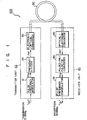
- Optical signal transmission system 100 mainly includes a transmitter unit 40, an optical fiber cable 50 and a receiver unit 60.
- Transmitter unit 40 is optically coupled via optical fiber cable 50 to receiver unit 60.
- Transmitter unit 40 includes a pulse frequency modulator (PFM modulator) 10 for PFM-modulating a transmission signal "St" as an input signal, a frequency divider 20 for frequency-dividing a PFM-modulated signal “Ptp” from modulator 10 at a predetermined frequency division ratio, and an electronic/optical converter 30 for converting a pulsed frequency modulated signal "Ptf” from divider 20 to an optical pulse signal, thereby transmitting the resultant transmission signal to optical fiber cable 50.
- PFM modulator pulse frequency modulator
- Receiver unit 60 coupled to transmitter unit 40 through optical fiber cable 50 includes an optical/electronic converter 90 for converting a received optical pulse signal (corresponding to the above transmission signal) to an electrical signal in order to obtain a rectangular pulse signal, a pulsed FM/pulse FM converter 80 for converting the pulsed FM signal "Prf” to a pulse frequency modulated signal, and a pulse frequency demodulator 70 for demodulating the resultant PFM signal as an original transmission signal or reception signal "Sr".
- an optical/electronic converter 90 for converting a received optical pulse signal (corresponding to the above transmission signal) to an electrical signal in order to obtain a rectangular pulse signal
- a pulsed FM/pulse FM converter 80 for converting the pulsed FM signal "Prf” to a pulse frequency modulated signal
- a pulse frequency demodulator 70 for demodulating the resultant PFM signal as an original transmission signal or reception signal "Sr".
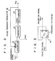
- pulse frequency modulator 10 as shown in Fig. 2 and frequency divider 20 as shown in Fig. 3 in combination with a waveform chart as shown in Fig. 4, production of pulsed FM signals, according to the invention, will be described in detail.
- a circuit arrangement of modulator 10 is shown in Fig. 2.
- Analog signals such as video and audio, and data signals are supplied, as transmission signal " S t" (Fig. 4), as discrete signals, or as a frequency-divided multiplexed signal, to integrator 12.
- Integrator 12 generates a sawtooth wave with a ramp corresponding to a voltage level of the input signal. In this case, the time required for charging an internal capacitor (not shown in detail) in integrator 12 to a predetermined level is proportional to the input voltage.
- An output signal from integrator 12 is compared in comparator 14 with reference voltage Vref., The time required for inverting the output voltage from comparator 14 to "1" level is proportional to the level of the input signal.
- a binary signal from comparator 14 is processed in mono-multivibrator 15 to have a predetermined pulse width, thus producing the pulse FM signal "Ptp” shown in Fig. 4. It can be seen that the pulse frequency of the pulse FM signal “Ptp” is changed, but its pulse width remains constant.
- the pulse FM signal "Ptp” is fed,back to integrator 12, functioning as a reset signal thereto.
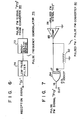
- Divider 20 includes, for example, D-type flip-flop 22, as shown in Fig. 3.
- the pulse FM signal "Ptp" from modulator 10 is supplied to the clock terminal CK of flip-flop 22.
- Data terminal D of flip-flop 22 is interconnected to output terminal Q. Therefore, the output from frequency divider 20 is derived as the pulsed FM signal "Ptf" at output terminal Q of flip-flop 22 (see Fig. 4).
- a frequency division ratio of divider 20 is set to be 1/2.
- the transmission signal "St" obtained by properly processing video or audio signals is first pulse FM modulated, and the resultant pulse FM signal “Ptp” is frequency-divided to produce a high-quality pulsed FM signal "Ptf".
- the pulsed FM signal "Ptf" is easily produced in the simple circuit arrangement described above.
- the resultant pulsed FM signal "Ptf” is then converted by electronic/optical converter 30 into an optical signal (not shown, but analogous to the pulsed FM signal "Ptf”).
- the optical signal is subsequently transmitted to receiver unit 60 through optical fiber cable 50.
- the optical pulsed FM signal transmitted through optical fiber cable 50 undergoes considerable transmission distortions and adverse effects from noises.
- the transmitted optical signal is received by receiver unit 60 and converted by optical/electronic converter 90 to a pulsed FM signal "Prf".
- the pulsed FM signal "Prf” is supplied to pulsed FM/pulse FM converter 80 (shown in Fig. 5).
- the received pulsed FM signal "Prf” and a delayed pulsed FM signal "Drf" (shown in Fig. 6), obtained by delaying the pulsed FM signal "Prf” in a delay circuit 82 for a predetermined time Td, are compared in an exclusive OR circuit 84.
- An output from exclusive OR circuit 84 serves as a pulse FM signal "Prp" with the pulse width shown in Fig. 4, that is, as the converted pulsed FM signal.
- the pulse FM signal "Prp” is demodulated in pulse frequency demodulator 79.
- Demodulator 79 includes a mono-multivibrator 72 and a low-pass filter 74, as shown in Fig. 6.
- the pulse FM signal "Prp” from converter 80 is subjected by mono-multivibrator 72 to pulse width regulation. Only the baseband components of the pulse FM signal with a predetermined pulse width are extracted by low-pass filter 74, thus obtaining original transmission signal or reception signal "Sr".
- the pulse frequency modulated signal is obtained before production of the pulsed FM signal.
- the pulse FM signal can be demodulated under the improved linearity by integrator 12 and comparator 14.
- integrator 12 when a time constant of integrator 12 is set arbitrarily, a variable frequency width is easily increased. Therefore, the pulsed FM signal produced by the system of this embodiment is a signal with the improved linearity and a high degree of demodulation.
- only a frequency divider is used to derive the pulsed FM signal from the pulse FM signal, thus avoiding complex circuitry.
- the received pulsed frequency modulated signal is not demodulated directly but demodulated after the reception signal is converted into the pulse FM signal. Since the baseband components excluded from the pulsed FM signal are included in the pulse FM signal, the baseband components can be filtered through the low-pass filter to achieve demodulation. Therefore, the circuit arrangement can be further simplified by employing such a demodulation manner.
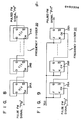
- a comparator 85 is arranged between optical/electronic converter 90 and converter 80. As seen from Fig. 7, since its arrangement and operation are well known, a detailed description thereof will be omitted.
- Model ECL F100107 available from Fairchild Inc. is employed as exclusive OR circuit 84, and its typical pin numbers 16, 17 and 18 are shown in Fig. 7.
- Frequency divider 20 shown in Fig. 3 is single stage D-type flip-flop 22.
- the number of frequency division stages may be determined arbitrarily.
- n D-type flip-flops 24A, 24B,... 24n can be arranged to frequency-divide the pulse FM signal "Ptp" at a ratio of l/(n+l).
- frequency divider 20 may be constituted by n J-K flip-flops 26A, 26B,... 26n.
- one-stage J-K flip-flop 28 shown in Fig. 10 may be used in place of one-stage D-type flip-flop 22 of Fig. 3.
- model ECL F100131 available from Fairchild Inc. is used as frequency divider 20, as shown in Fig. 11.
- Typical pin numbers 13 to 16 are written in the same manner as in Fig. 7.
- the frequency division ratio of frequency divider 20 can be set arbitrarily.
- a frequency division ratio of 1/2 i.e., a one-stage flip-flop
- the center frequency and frequency deviation of the input pulse FM signal is known to be improved as compared with other frequency dividers, e.g., 1/4 and 1/8 dividers.
- the pulse frequency modulator has a wider variable frequency range and improved linearity within this variable range, and is substantially free from modulation distortion.
- a pulse FM signal with a high degree of modulation can be obtained.
- the pulsed FM signal can be obtained by simply frequency-dividing the pulse FM signal into a predetermined number of stages, the resultant pulsed FM signal has high quality.
- the pulse frequency modulator and the frequency divider can be constituted by very simple circuits, which eliminates the need of a complicated transmitter unit configuration.
- the pulsed FM signal is first converted to the pulse FM signal by the receiver unit, demodulation can be performed simply by filtering the baseband components included in the pulse FM signal through the low-pass filter. Therefore, the arrangement of the receiver unit can also be simplified.
- the transmitter and receiver units are simplified, and high-quality pulsed FM signals with high frequency band-utilization efficiency can be transmitted.
- the pulsed FM signal is converted by the delay detection circuit (including the delay and exclusive OR circuits) into the pulse FM signal.
- the pulse train of the pulse FM signal is alternately generated as a pair at the leading and trailing edge portions of the pulsed FM signal.
- noises e.g., sinusoidal noises
- the pair of pulse FM pulses are shifted in opposite directions, and the influence of the noises does not appear at the output of the low-pass filter.
- the baseband components do not influence the demodulated output.
Landscapes
- Engineering & Computer Science (AREA)
- Computer Networks & Wireless Communication (AREA)
- Signal Processing (AREA)
- Physics & Mathematics (AREA)
- Electromagnetism (AREA)
- Optical Communication System (AREA)
- Digital Transmission Methods That Use Modulated Carrier Waves (AREA)
Applications Claiming Priority (2)
| Application Number | Priority Date | Filing Date | Title |
|---|---|---|---|
| JP39298/85 | 1985-02-28 | ||
| JP60039298A JPS61198935A (ja) | 1985-02-28 | 1985-02-28 | 光伝送方式 |
Publications (3)
| Publication Number | Publication Date |
|---|---|
| EP0193396A2 true EP0193396A2 (de) | 1986-09-03 |
| EP0193396A3 EP0193396A3 (en) | 1988-12-14 |
| EP0193396B1 EP0193396B1 (de) | 1992-07-08 |
Family
ID=12549223
Family Applications (1)
| Application Number | Title | Priority Date | Filing Date |
|---|---|---|---|
| EP86301381A Expired - Lifetime EP0193396B1 (de) | 1985-02-28 | 1986-02-26 | Optisches Signalübertragungssystem mit Pulsfrequenzmodulations-Modem |
Country Status (5)
| Country | Link |
|---|---|
| US (1) | US4928318A (de) |
| EP (1) | EP0193396B1 (de) |
| JP (1) | JPS61198935A (de) |
| CA (1) | CA1238687A (de) |
| DE (1) | DE3685890T2 (de) |
Cited By (1)
| Publication number | Priority date | Publication date | Assignee | Title |
|---|---|---|---|---|
| FR2733651A1 (fr) * | 1995-04-26 | 1996-10-31 | Sextant Avionique | Procede et dispositif pour la transmission de signaux analogiques au moyen d'un systeme de transmission utilisant des lignes de transmission optique |
Families Citing this family (14)
| Publication number | Priority date | Publication date | Assignee | Title |
|---|---|---|---|---|
| JP2751162B2 (ja) * | 1987-09-11 | 1998-05-18 | 日本電気株式会社 | 光伝送方式 |
| JPS6486727A (en) * | 1987-09-29 | 1989-03-31 | Omron Tateisi Electronics Co | Optical analog transmission module |
| JPH0276486A (ja) * | 1988-09-13 | 1990-03-15 | Pioneer Electron Corp | 映像信号の光伝送システム |
| US5132957A (en) * | 1988-11-07 | 1992-07-21 | Teac Corporation | Information signal recording and reproducing system capable of recording an information signal on a medium having a limited recording band width |
| DE69019846T2 (de) * | 1989-03-09 | 1995-12-07 | Canon Kk | Optisches Übertragungssystem. |
| DE59008497D1 (de) * | 1989-04-20 | 1995-03-30 | Siemens Ag | Übertragungsstrecke. |
| KR920014231A (ko) * | 1990-12-31 | 1992-07-30 | 이헌조 | 무선헤드폰 송 수신회로 |
| US5586145A (en) * | 1993-01-11 | 1996-12-17 | Morgan; Harry C. | Transmission of electronic information by pulse position modulation utilizing low average power |
| DE69636981T2 (de) * | 1995-11-29 | 2007-12-06 | Koninklijke Philips Electronics N.V. | Übertragungssystem für ein nichtlineares übertragungsmedium |
| US5737140A (en) * | 1996-06-07 | 1998-04-07 | Eastman Kodak Company | Simple pulse position modulation channel/decoder |
| WO1998028847A1 (en) * | 1996-12-23 | 1998-07-02 | Dsc Communications A/S | A method and a circuit for the transfer of data information |
| DE19737482A1 (de) * | 1997-08-28 | 1999-03-04 | Alsthom Cge Alcatel | Verfahren zur optischen Übertragung über ein Lichtwellenleiternetz, sowie optisches Übertragungsnetz |
| US6735398B1 (en) * | 2000-03-15 | 2004-05-11 | Hughes Electronics Corporation | Generating methods for single and multi-channel wideband optical analog pulse positioned waveforms |
| PL3500865T3 (pl) * | 2016-08-22 | 2024-04-29 | The University Of Sydney | Optyczny analizator widma rf |
Family Cites Families (3)
| Publication number | Priority date | Publication date | Assignee | Title |
|---|---|---|---|---|
| US4399564A (en) * | 1980-02-19 | 1983-08-16 | The United States Of America As Represented By The Secretary Of The Navy | Fiber optic system for transmission of video signals by pulse-frequency-modulation |
| FR2485294A1 (fr) * | 1980-06-23 | 1981-12-24 | Trt Telecom Radio Electr | Demodulateur de frequence utilisant un circuit a retard variable avec la frequence recue |
| JPS60170359A (ja) * | 1984-02-14 | 1985-09-03 | Meidensha Electric Mfg Co Ltd | V/f変換デ−タ伝送装置 |
-
1985
- 1985-02-28 JP JP60039298A patent/JPS61198935A/ja active Pending
-
1986
- 1986-02-24 CA CA000502556A patent/CA1238687A/en not_active Expired
- 1986-02-26 EP EP86301381A patent/EP0193396B1/de not_active Expired - Lifetime
- 1986-02-26 DE DE8686301381T patent/DE3685890T2/de not_active Expired - Fee Related
-
1987
- 1987-12-22 US US07/136,534 patent/US4928318A/en not_active Expired - Fee Related
Cited By (2)
| Publication number | Priority date | Publication date | Assignee | Title |
|---|---|---|---|---|
| FR2733651A1 (fr) * | 1995-04-26 | 1996-10-31 | Sextant Avionique | Procede et dispositif pour la transmission de signaux analogiques au moyen d'un systeme de transmission utilisant des lignes de transmission optique |
| WO1996034465A1 (fr) * | 1995-04-26 | 1996-10-31 | Sextant Avionique | Procede et dispositif pour la transmission de signaux analogiques au moyen d'un systeme de transmission utilisant des lignes de transmission optique |
Also Published As
| Publication number | Publication date |
|---|---|
| CA1238687A (en) | 1988-06-28 |
| EP0193396B1 (de) | 1992-07-08 |
| JPS61198935A (ja) | 1986-09-03 |
| DE3685890T2 (de) | 1993-02-18 |
| EP0193396A3 (en) | 1988-12-14 |
| DE3685890D1 (de) | 1992-08-13 |
| US4928318A (en) | 1990-05-22 |
Similar Documents
| Publication | Publication Date | Title |
|---|---|---|
| EP0193396B1 (de) | Optisches Signalübertragungssystem mit Pulsfrequenzmodulations-Modem | |
| US4893341A (en) | Digital receiver operating at sub-nyquist sampling rate | |
| JPH07154287A (ja) | 直接変換受信機 | |
| JPS6310823A (ja) | 位相ロックル−プ・システム | |
| US4907092A (en) | Modulating/demodulating circuit for multiplex recording/playback of data in a magnetic recording/playback system | |
| US4639911A (en) | Head-end and receiver for a signal distribution system | |
| DK168846B1 (da) | Fremgangsmåde ved og apparat til signalregistrering, registreringsbærer med et i overensstemmelse hermed registreret signal, samt apparat til signalgengivelse | |
| US4475217A (en) | Receiver for phase-shift modulated carrier signals | |
| US3594509A (en) | Delta modulator apparatus | |
| US4744094A (en) | BPSK demodulator with D type flip/flop | |
| GB2031693A (en) | Timing signal extraction system | |
| CA1066782A (en) | Receiver for synchronous signals with double phase-locked loop | |
| US4622683A (en) | Fast acquisition ringing filter MSK demodulator | |
| US4780893A (en) | Bit synchronizer | |
| US5020079A (en) | Apparatus for generating a minimum-shift-keying signal | |
| US3863264A (en) | Sequential color and memory decoder | |
| US5850161A (en) | Digital FM demodulator using pulse generators | |
| US4479099A (en) | Multiple phase modulator for N sets of digital data | |
| US4547751A (en) | System for frequency modulation | |
| US4660097A (en) | Color video system with digital audio pulse width modulation | |
| EP0534180B1 (de) | Demodulatorschaltung für MSK-Signale | |
| HK3594A (en) | Compatible increase of the definition in a colour television system | |
| JP2803721B2 (ja) | ビットレートフリー光受信器 | |
| US3949417A (en) | Sequential color and memory decoder | |
| JP2529375B2 (ja) | パルス多重伝送方式における復調回路 |
Legal Events
| Date | Code | Title | Description |
|---|---|---|---|
| PUAI | Public reference made under article 153(3) epc to a published international application that has entered the european phase |
Free format text: ORIGINAL CODE: 0009012 |
|
| AK | Designated contracting states |
Kind code of ref document: A2 Designated state(s): DE FR GB |
|
| 17P | Request for examination filed |
Effective date: 19861010 |
|
| PUAL | Search report despatched |
Free format text: ORIGINAL CODE: 0009013 |
|
| AK | Designated contracting states |
Kind code of ref document: A3 Designated state(s): DE FR GB |
|
| 17Q | First examination report despatched |
Effective date: 19910116 |
|
| GRAA | (expected) grant |
Free format text: ORIGINAL CODE: 0009210 |
|
| AK | Designated contracting states |
Kind code of ref document: B1 Designated state(s): DE FR GB |
|
| REF | Corresponds to: |
Ref document number: 3685890 Country of ref document: DE Date of ref document: 19920813 |
|
| ET | Fr: translation filed | ||
| PLBE | No opposition filed within time limit |
Free format text: ORIGINAL CODE: 0009261 |
|
| 26N | No opposition filed | ||
| REG | Reference to a national code |
Ref country code: GB Ref legal event code: 746 Effective date: 19981007 |
|
| REG | Reference to a national code |
Ref country code: FR Ref legal event code: D6 |
|
| PGFP | Annual fee paid to national office [announced via postgrant information from national office to epo] |
Ref country code: DE Payment date: 19991231 Year of fee payment: 15 |
|
| PGFP | Annual fee paid to national office [announced via postgrant information from national office to epo] |
Ref country code: FR Payment date: 20000210 Year of fee payment: 15 |
|
| PGFP | Annual fee paid to national office [announced via postgrant information from national office to epo] |
Ref country code: GB Payment date: 20000223 Year of fee payment: 15 |
|
| PG25 | Lapsed in a contracting state [announced via postgrant information from national office to epo] |
Ref country code: GB Free format text: LAPSE BECAUSE OF NON-PAYMENT OF DUE FEES Effective date: 20010226 |
|
| GBPC | Gb: european patent ceased through non-payment of renewal fee |
Effective date: 20010226 |
|
| PG25 | Lapsed in a contracting state [announced via postgrant information from national office to epo] |
Ref country code: FR Free format text: LAPSE BECAUSE OF NON-PAYMENT OF DUE FEES Effective date: 20011031 |
|
| REG | Reference to a national code |
Ref country code: FR Ref legal event code: ST |
|
| PG25 | Lapsed in a contracting state [announced via postgrant information from national office to epo] |
Ref country code: DE Free format text: LAPSE BECAUSE OF NON-PAYMENT OF DUE FEES Effective date: 20011201 |