EP0194939A2 - Dispositif de mémoire semi-conducteur - Google Patents
Dispositif de mémoire semi-conducteur Download PDFInfo
- Publication number
- EP0194939A2 EP0194939A2 EP86400504A EP86400504A EP0194939A2 EP 0194939 A2 EP0194939 A2 EP 0194939A2 EP 86400504 A EP86400504 A EP 86400504A EP 86400504 A EP86400504 A EP 86400504A EP 0194939 A2 EP0194939 A2 EP 0194939A2
- Authority
- EP
- European Patent Office
- Prior art keywords
- output
- output buffer
- buffer stages
- data
- memory device
- Prior art date
- Legal status (The legal status is an assumption and is not a legal conclusion. Google has not performed a legal analysis and makes no representation as to the accuracy of the status listed.)
- Granted
Links
Images


Classifications
-
- G—PHYSICS
- G11—INFORMATION STORAGE
- G11C—STATIC STORES
- G11C11/00—Digital stores characterised by the use of particular electric or magnetic storage elements; Storage elements therefor
- G11C11/21—Digital stores characterised by the use of particular electric or magnetic storage elements; Storage elements therefor using electric elements
- G11C11/34—Digital stores characterised by the use of particular electric or magnetic storage elements; Storage elements therefor using electric elements using semiconductor devices
-
- G—PHYSICS
- G11—INFORMATION STORAGE
- G11C—STATIC STORES
- G11C7/00—Arrangements for writing information into, or reading information out from, a digital store
- G11C7/10—Input/output [I/O] data interface arrangements, e.g. I/O data control circuits, I/O data buffers
- G11C7/1051—Data output circuits, e.g. read-out amplifiers, data output buffers, data output registers, data output level conversion circuits
- G11C7/1057—Data output buffers, e.g. comprising level conversion circuits, circuits for adapting load
-
- G—PHYSICS
- G11—INFORMATION STORAGE
- G11C—STATIC STORES
- G11C7/00—Arrangements for writing information into, or reading information out from, a digital store
- G11C7/10—Input/output [I/O] data interface arrangements, e.g. I/O data control circuits, I/O data buffers
- G11C7/1051—Data output circuits, e.g. read-out amplifiers, data output buffers, data output registers, data output level conversion circuits
- G11C7/106—Data output latches
-
- G—PHYSICS
- G11—INFORMATION STORAGE
- G11C—STATIC STORES
- G11C7/00—Arrangements for writing information into, or reading information out from, a digital store
- G11C7/22—Read-write [R-W] timing or clocking circuits; Read-write [R-W] control signal generators or management
Definitions
- the present invention relates to a semiconductor memory device. More particularly, it relates to a semiconductor memory device having a multi-bit constitution, in which the output buffer stages are driven by each sequential output of the delay control means and a sequential time-delayed signals are output by the output buffer stage to prevent a rush current from flowing at the beginning of the data output and to eliminate a malfunction in a memory device and associated circuits thereof.
- a semiconductor memory device such as a dynamic RAM having multi-bit output stages constituted by, e:g., 16 K x 4 bits or 8 K x 8 bits
- a large current flows through a line from the positive side power source line to the output terminal or through a line from the output terminal to the ground side power source line during the period in which the output is changed from a low level to a high level, or vice versa.
- This excessive transient current is likely to cause a fluctuation of the potential at the positive side power source line or at the ground side source line. The fluctuation is due to insufficient capacity of the power source and parasitic resistance of the power source line, and thus causes a malfunction in the semiconductor memory device itself or in its associated circuits.
- the fluctuation of the potential along the ground side power source line is undesirable to avoid malfunctions because this line is usually used as a reference potential line which determines the logic levels of signals.
- This problem is serious in memory devices of multi-bit type which generates plural output data signals at a time in response to address signals for one address.
- the output buffers contained in the device for generating the data outputs should have sufficient ability of driving external lines for fast read-out operation, resulting in undesirable amount of potential fluctuation along the power source lines particularly when all the data outputs at a time have the same polarity.
- An object of the present invention is to provide a semiconductor memory device including a plurality of output buffer stages to reduce malfunctions of the memory circuit and associated circuits thereof, by eliminating the multiplication of the transient current by those output stages which would otherwise cause a significant rise in the potential level of the power source line.
- a semiconductor memory device of multi-bit type which produce plural output signals corresponding to readout data from one address at a time, including memory means for storing data; a plurality of output buffer stages for producing the output signals, the operation of the output buffer stages being based upon-at least a timing signal; and means for operating the output buffer stages with predetermined time differences.
- the output signals having predetermined time differences are delivered from the output buffer stages.
- Figure 1 is a schematic block diagram of a semiconductor memory device according to an embodiment of the present invention.
- 111 denotes a flip-flop circuit
- 121 an output stage in the form of an inverter.
- BOT(l), BOT(2), ... BOT(n) denote output buffer circuits.
- 131 denotes an output switching circuit, 141 an inverter, 151 a delay circuit, 161 an inverter and 171 a NOR gate.
- 181 denotes a data output terminal.
- Ql, Q2, Q5, Q6 and Q8, Q9 are pairs of transistors each constituting an inverter, respectively;
- Q3 is an output switching transistor;
- Q4 a charge discharging switching transistor;
- Q7 a transistor forming a delay circuit;
- Q10, Qll, Q12, and Q13 are transistors forming a NOR gate.
- CT is a MOS type capacitor forming a delay circuit, and D(OUT)1 to D(OUT)n are data output terminals for each output buffer BOT(l) to BOT(n).
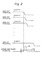
- Figure 2 is a diagram showing the transition of the potential level of data output in the data output terminals D(OUT)1 to D(OUT)n and the potential level of the ground side power source V SS .
- the flip-flop 111 storing data Dl read out from the memory cell array sends an output caused by a trigger pulse ⁇ to an output stage 121.
- other flip-flop circuits 112, 113, ... lln storing data D2, D3, ... Dn send outputs at the same time by the trigger pulse ⁇ to the corresponding output stages 122, 123, ... 12n.
- each switching transistor Ql and Q3 is ON.
- an "H" potential level is output from the output terminals D(OUT)1 to D(OUT)n and each capacitor is charged. In this case the delay action is not effected by the output buffer circuit BOT(l).
- the data output D 01 from the output stage 121 is made "H" through an inverter 141 formed by transistors Q5 and Q6, and applied to the delay circuit 151.
- the transistor Q7 is a depletion type and acts as a constant current source, rendering a constant current flow by degrees to a MOS capacitor CT and thus a gradual charging thereof.
- an inverter 161 formed by transistors Q8 and Q9 operates, and the output of the inverter being "L” is then applied to a NOR gate circuit 171 formed by transistors Q10, Q11, Q12 and Q13.
- the output D017 of the NOR gate circuit 171 is "H" and a switching transistor Q4 is made ON, and thus a charge stored in the capacitor C is discharged through the switching transistor Q4.
- the discharge i.e., the trailing of the output data
- each delay circuit 151 in each output buffer is provided with a different time constant from each other, leading to difference in timing of turn-on of the transistor Q 4 in each output buffer. Therefore, as can be seen in Fig. 2, the variation ⁇ H of the potential.level of the ground side power source line is small and slow.
- Fig. 2 shows a comparison between the present invention and the prior art. Due to the time shift discharge, comparatively little peak current flows, and in response, the height AH of the rise of ground side source potential V SS is low. Whereas, in the prior art, a rush current flows and the corresponding rise of ground side source potential V SS ' is abrupt and high.
- read-out data D 2 , ... D n are transferred in parallel from the memory cell array to flip-flops, delivered by a trigger pulse ⁇ to each inverters 121, ... 12n, then transferred to each of the output buffers BOT(l), BOT(2), ... BOT(n), and the data outputs D(OUT)1, ... D(OUT)n are fetched out.
- the output voltage V in the delay circuit 151 is approximately expressed by the equation, V V CC (1 - e -t /T), where T is a time constant in the delay circuit.
- V INV the voltage inverted by an inverter
- the device of Fig. 1 provides the output stages to which the loads including capacitance are connected, and the output buffer circuits connected to the output stages and having the output switching circuits, the inverter circuits, the delay circuits, and NOR gates.
- the time-divisional discharge of the capacitor is attained by the output switching circuit including the transistors Q3 and Q4 and the delay circuits.
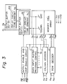
- a semiconductor memory device according to another embodiment of the present invention is shown in Fig. 4. This embodiment is particularly suitable for n-channel dynamic MOS memory devices.
- 301, 302, 303, 304 are flip-flops, DBl, DB1 , DB2, DB2 , DB3, DB3 , and DB4, DB4 are pairs of input terminals, 211, 212, 213 and 214 push-pull buffers, DQl, DQ2, DQ3 and DQ4 outputs, 251, 252 and 253 delay circuits, and 0 , ⁇ 1 , ⁇ 2 , and ⁇ 3 trigger pulses or clock inputs.
- V CC denotes a positive side power source voltage
- V SS the ground side voltage. All the transistors depicted are of n-channel type.
- Each memory or flip-flop 301 to 304 is activated to latch data input through the input terminal by a clock pulse ⁇ 0 , ... ⁇ 3 .
- the flip-flops 301, ... 304 drive the push-pull buffers 211 to 214, respectively, only while activated. Otherwise, the push-pull buffers 211 to 214 are maintained in a high impedance (High-Z) state.
- Each clock pulse ⁇ 0 , ⁇ 1 , ⁇ 2 , and ⁇ 3 is applied to the flip-flops 301, ... 304 with a definite time delay, and then the output of the flip-flop 301, that is, A 1 or B 1 , A 2 or B 2 , A3 or B 3 , and A4 or B 4 , is generated and delivered to the push-pull buffers 211 to 214.
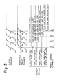
- the waveform of the outputs DQl to DQ4 of each buffer 211 to 214 is shown in Fig. 5.
- the flip-flop 301 is disabled, both Al and Bl are low and the buffer 211 is in High-Z state.
- ⁇ 0 is input, then Al becomes High and Bl becomes Low, or Bl becomes High, and Al becomes Low in correspondence with the read-out data.
- the input terminals A or B 1 , A 2 or B2 , A3 or B 3 , and A4 or B 4 in the output stage or in the buffer stages 211 to 214 are raised and all the times at which the outputs appear are time-shifted. Accordingly, a much current cannot flow at a time from the power source, and the peak current is divided into l/(n + 1), where n is the number of delay circuits. Thus, a noise or disturbance signal due to such a rush current is not superimposed on the power source line and accordingly, the possibility of a malfunction of the memory circuit and associated circuits is reduced.
- delay circuits having different time constants are provided, and thus the semiconductor memory device according to the present invention is provided with the ability of interposing each delay circuit with a different time constant on the input terminal sides of the output stages of multi-bit type, to start the operation of data outputs at separate times from each output stage.
- the memory device includes a multi-bit output stage, rush current does not flow at the time of data output, thus eliminating the risk that a malfunction will occur in the memory or an associated circuit.
- Figures 6 and 3 are block diagrams giving details of the embodiments shown in Figs. 1 and 4.
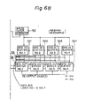
- Figure 6 is a block diagram of a dynamic RAM (DRAM).
- the output of the DRAM is done by the multi-bit type buffers for data out.
- a row address strobe RAS is input to a clock generator No. 1 and a column address strobe CAS is introduced into a clock generator No. 2 through a gate.
- the outputs of the clock generators No. 1 and No. 2 are sent to address buffers, and another output of the clock generator No. ⁇ 1 drives a reference control clock and the output is counted by an internal refresh address counter, the count output is then delivered to the address buffer.
- These are used only in the refresh mode and the explanation is omitted.
- Two sets of predetermined eight address A 0 to A 7 are applied to the address buffer by the control of the strobe signals RAS and CAS and the two outputs are generated.
- One output is sent to a column decoder and the other to a row decoder.
- the address is stored in a 262,144-bit storage which has a format of 64 K words x 4 bits.
- a write enable signal WE drives a write clock generator and the output is distributed among the data-in buffers No. 1 to No. 4.
- the output of the clock generator No. 1 is sent to sense amplifiers and the outputs thereof are fed to data-in buffers No. 1 to No. 4.
- the output of the clock generator No. 2 are sent to a column decoder and data-out buffer No. 1.
- the output enable signals are delivered to the data-out buffers No. 1 to No. 4.
- the outputs of the data-out buffers are fetched through the external pins as the output.
- the delay circuits are, respectively, connected to the data out buffers.
- the function of the delay circuits is the same as in Fig. 1.
- Fig. 3 is a block diagram of an EPROM using output delay circuits with a different time constant, as a second embodiment according to the present invention.
- An output enable signal OE and a chip enable signal CE are input to an output enable and chip enable circuit and the output is delivered to a data input buffer, a column decoder, a row decoder, and output buffers No. 1 to No. 8.
- the outputs of a column and row decoder are sent to a memory cell array, and the address is assigned.
- the output read out from the memory cell array is delivered to output buffers No. 1 to No. 8 and outputs in response to a predetermined time constant are provided.
Landscapes
- Engineering & Computer Science (AREA)
- Computer Hardware Design (AREA)
- Dram (AREA)
- Logic Circuits (AREA)
Applications Claiming Priority (4)
| Application Number | Priority Date | Filing Date | Title |
|---|---|---|---|
| JP49350/85 | 1985-03-14 | ||
| JP4935085 | 1985-03-14 | ||
| JP54666/85 | 1985-03-20 | ||
| JP5466685 | 1985-03-20 |
Publications (3)
| Publication Number | Publication Date |
|---|---|
| EP0194939A2 true EP0194939A2 (fr) | 1986-09-17 |
| EP0194939A3 EP0194939A3 (en) | 1988-12-21 |
| EP0194939B1 EP0194939B1 (fr) | 1992-02-05 |
Family
ID=26389736
Family Applications (1)
| Application Number | Title | Priority Date | Filing Date |
|---|---|---|---|
| EP86400504A Expired - Lifetime EP0194939B1 (fr) | 1985-03-14 | 1986-03-11 | Dispositif de mémoire semi-conducteur |
Country Status (4)
| Country | Link |
|---|---|
| US (1) | US4802127A (fr) |
| EP (1) | EP0194939B1 (fr) |
| KR (1) | KR910000876B1 (fr) |
| DE (1) | DE3683783D1 (fr) |
Cited By (2)
| Publication number | Priority date | Publication date | Assignee | Title |
|---|---|---|---|---|
| EP0316082A3 (fr) * | 1987-10-28 | 1991-03-27 | Kabushiki Kaisha Toshiba | Tampon d'entrée et de sortie pour circuit intégré |
| EP0686975A1 (fr) * | 1989-12-14 | 1995-12-13 | Kabushiki Kaisha Toshiba | Circuit de tampon de sortie de données pour circuit intégré à semi-conducteurs |
Families Citing this family (12)
| Publication number | Priority date | Publication date | Assignee | Title |
|---|---|---|---|---|
| US5030853A (en) * | 1990-03-21 | 1991-07-09 | Thunderbird Technologies, Inc. | High speed logic and memory family using ring segment buffer |
| US5105105A (en) * | 1990-03-21 | 1992-04-14 | Thunderbird Technologies, Inc. | High speed logic and memory family using ring segment buffer |
| IL96808A (en) * | 1990-04-18 | 1996-03-31 | Rambus Inc | Introductory / Origin Circuit Agreed Using High-Performance Brokerage |
| US5208776A (en) * | 1990-07-31 | 1993-05-04 | Texas Instruments, Incorporated | Pulse generation circuit |
| JP2605565B2 (ja) * | 1992-11-27 | 1997-04-30 | 日本電気株式会社 | 半導体集積回路 |
| US5500818A (en) * | 1993-10-29 | 1996-03-19 | Sun Microsystems, Inc. | Method and apparatus for providing accurate T(on) and T(off) times for the output of a memory array |
| KR960013858B1 (ko) * | 1994-02-03 | 1996-10-10 | 현대전자산업 주식회사 | 데이타 출력버퍼 제어회로 |
| JPH08263985A (ja) * | 1995-03-24 | 1996-10-11 | Nec Corp | 半導体記憶装置 |
| JP2888200B2 (ja) * | 1996-07-11 | 1999-05-10 | 日本電気株式会社 | 半導体装置 |
| DE19741426C1 (de) * | 1997-09-19 | 1999-01-21 | Siemens Ag | Schaltungsanordnung zur Datenspeicherung |
| US6459313B1 (en) | 1998-09-18 | 2002-10-01 | Lsi Logic Corporation | IO power management: synchronously regulated output skew |
| US7965728B2 (en) * | 2006-11-14 | 2011-06-21 | St-Ericsson Sa | Buffer for driving capacitive load |
Family Cites Families (5)
| Publication number | Priority date | Publication date | Assignee | Title |
|---|---|---|---|---|
| JPS57152589A (en) * | 1981-03-13 | 1982-09-20 | Fujitsu Ltd | Semiconductor memory |
| JPS58128089A (ja) * | 1981-12-26 | 1983-07-30 | Fujitsu Ltd | 半導体記憶装置 |
| JPS59181829A (ja) * | 1983-03-31 | 1984-10-16 | Toshiba Corp | 半導体素子の出力バツフア回路 |
| JPS6020387A (ja) * | 1983-07-15 | 1985-02-01 | Nec Corp | メモリ回路 |
| JPS60115092A (ja) * | 1983-11-28 | 1985-06-21 | Nec Corp | 半導体記憶回路 |
-
1986
- 1986-03-11 EP EP86400504A patent/EP0194939B1/fr not_active Expired - Lifetime
- 1986-03-11 DE DE8686400504T patent/DE3683783D1/de not_active Expired - Lifetime
- 1986-03-14 KR KR1019860001865A patent/KR910000876B1/ko not_active Expired
-
1988
- 1988-05-18 US US07/196,772 patent/US4802127A/en not_active Expired - Lifetime
Cited By (2)
| Publication number | Priority date | Publication date | Assignee | Title |
|---|---|---|---|---|
| EP0316082A3 (fr) * | 1987-10-28 | 1991-03-27 | Kabushiki Kaisha Toshiba | Tampon d'entrée et de sortie pour circuit intégré |
| EP0686975A1 (fr) * | 1989-12-14 | 1995-12-13 | Kabushiki Kaisha Toshiba | Circuit de tampon de sortie de données pour circuit intégré à semi-conducteurs |
Also Published As
| Publication number | Publication date |
|---|---|
| US4802127A (en) | 1989-01-31 |
| KR910000876B1 (ko) | 1991-02-11 |
| EP0194939B1 (fr) | 1992-02-05 |
| DE3683783D1 (de) | 1992-03-19 |
| EP0194939A3 (en) | 1988-12-21 |
| KR860007744A (ko) | 1986-10-17 |
Similar Documents
| Publication | Publication Date | Title |
|---|---|---|
| US4161040A (en) | Data-in amplifier for an MISFET memory device having a clamped output except during the write operation | |
| US4918339A (en) | Data output circuit | |
| US4983860A (en) | Data output buffer for use in semiconductor device | |
| US6061295A (en) | Integrated circuit memory devices having time compensated column selection capability for improving write operation reliability | |
| US4087704A (en) | Sequential timing circuitry for a semiconductor memory | |
| US4322635A (en) | High speed serial shift register for MOS integrated circuit | |
| US4592026A (en) | Memory device resistant to soft errors | |
| EP0125699A2 (fr) | Circuit de sortie de données pour un dispositif de mémoire dynamique | |
| US4449207A (en) | Byte-wide dynamic RAM with multiplexed internal buses | |
| US4802127A (en) | Output buffer circuit for a semiconductor memory device | |
| EP0069588A2 (fr) | Circuit de mémoire semi-conductrice intégrée | |
| US4099265A (en) | Sense line balance circuit for static random access memory | |
| US4754170A (en) | Buffer circuit for minimizing noise in an integrated circuit | |
| JPS63166090A (ja) | スタティック型メモリ | |
| JPS6214520A (ja) | メモリの出力バツフア回路 | |
| US3938109A (en) | High speed ECL compatible MOS-Ram | |
| US4281401A (en) | Semiconductor read/write memory array having high speed serial shift register access | |
| US20010026474A1 (en) | Semiconductor storage device | |
| US4338679A (en) | Row driver circuit for semiconductor memory | |
| US4455627A (en) | Static type semiconductor memory device | |
| EP0115140B1 (fr) | Circuit décodeur | |
| US5270978A (en) | Nonvolatile memory circuit | |
| KR950014256B1 (ko) | 낮은 전원전압을 사용하는 반도체 메모리장치 | |
| EP0031995B1 (fr) | Dispositif de mémoire à semi-conducteurs comprenant une matrice de cellules de mémoire statiques | |
| US5343433A (en) | CMOS sense amplifier |
Legal Events
| Date | Code | Title | Description |
|---|---|---|---|
| PUAI | Public reference made under article 153(3) epc to a published international application that has entered the european phase |
Free format text: ORIGINAL CODE: 0009012 |
|
| AK | Designated contracting states |
Kind code of ref document: A2 Designated state(s): DE FR GB |
|
| PUAL | Search report despatched |
Free format text: ORIGINAL CODE: 0009013 |
|
| AK | Designated contracting states |
Kind code of ref document: A3 Designated state(s): DE FR GB |
|
| 17P | Request for examination filed |
Effective date: 19890304 |
|
| 17Q | First examination report despatched |
Effective date: 19900801 |
|
| GRAA | (expected) grant |
Free format text: ORIGINAL CODE: 0009210 |
|
| AK | Designated contracting states |
Kind code of ref document: B1 Designated state(s): DE FR GB |
|
| REF | Corresponds to: |
Ref document number: 3683783 Country of ref document: DE Date of ref document: 19920319 |
|
| ET | Fr: translation filed | ||
| PLBE | No opposition filed within time limit |
Free format text: ORIGINAL CODE: 0009261 |
|
| STAA | Information on the status of an ep patent application or granted ep patent |
Free format text: STATUS: NO OPPOSITION FILED WITHIN TIME LIMIT |
|
| 26N | No opposition filed | ||
| REG | Reference to a national code |
Ref country code: GB Ref legal event code: IF02 |
|
| PGFP | Annual fee paid to national office [announced via postgrant information from national office to epo] |
Ref country code: FR Payment date: 20020312 Year of fee payment: 17 |
|
| PGFP | Annual fee paid to national office [announced via postgrant information from national office to epo] |
Ref country code: GB Payment date: 20020313 Year of fee payment: 17 |
|
| PGFP | Annual fee paid to national office [announced via postgrant information from national office to epo] |
Ref country code: DE Payment date: 20020327 Year of fee payment: 17 |
|
| PG25 | Lapsed in a contracting state [announced via postgrant information from national office to epo] |
Ref country code: GB Free format text: LAPSE BECAUSE OF NON-PAYMENT OF DUE FEES Effective date: 20030311 |
|
| PG25 | Lapsed in a contracting state [announced via postgrant information from national office to epo] |
Ref country code: DE Free format text: LAPSE BECAUSE OF NON-PAYMENT OF DUE FEES Effective date: 20031001 |
|
| GBPC | Gb: european patent ceased through non-payment of renewal fee |
Effective date: 20030311 |
|
| PG25 | Lapsed in a contracting state [announced via postgrant information from national office to epo] |
Ref country code: FR Free format text: LAPSE BECAUSE OF NON-PAYMENT OF DUE FEES Effective date: 20031127 |
|
| REG | Reference to a national code |
Ref country code: FR Ref legal event code: ST |