EP0196905A2 - Flüssigkristall-Zellenadressierung - Google Patents
Flüssigkristall-Zellenadressierung Download PDFInfo
- Publication number
- EP0196905A2 EP0196905A2 EP86302382A EP86302382A EP0196905A2 EP 0196905 A2 EP0196905 A2 EP 0196905A2 EP 86302382 A EP86302382 A EP 86302382A EP 86302382 A EP86302382 A EP 86302382A EP 0196905 A2 EP0196905 A2 EP 0196905A2
- Authority
- EP
- European Patent Office
- Prior art keywords
- liquid crystal
- data
- pulses
- voltage
- pulse
- Prior art date
- Legal status (The legal status is an assumption and is not a legal conclusion. Google has not performed a legal analysis and makes no representation as to the accuracy of the status listed.)
- Ceased
Links
Images
Classifications
-
- G—PHYSICS
- G09—EDUCATION; CRYPTOGRAPHY; DISPLAY; ADVERTISING; SEALS
- G09G—ARRANGEMENTS OR CIRCUITS FOR CONTROL OF INDICATING DEVICES USING STATIC MEANS TO PRESENT VARIABLE INFORMATION
- G09G3/00—Control arrangements or circuits, of interest only in connection with visual indicators other than cathode-ray tubes
- G09G3/20—Control arrangements or circuits, of interest only in connection with visual indicators other than cathode-ray tubes for presentation of an assembly of a number of characters, e.g. a page, by composing the assembly by combination of individual elements arranged in a matrix no fixed position being assigned to or needed to be assigned to the individual characters or partial characters
- G09G3/34—Control arrangements or circuits, of interest only in connection with visual indicators other than cathode-ray tubes for presentation of an assembly of a number of characters, e.g. a page, by composing the assembly by combination of individual elements arranged in a matrix no fixed position being assigned to or needed to be assigned to the individual characters or partial characters by control of light from an independent source
- G09G3/36—Control arrangements or circuits, of interest only in connection with visual indicators other than cathode-ray tubes for presentation of an assembly of a number of characters, e.g. a page, by composing the assembly by combination of individual elements arranged in a matrix no fixed position being assigned to or needed to be assigned to the individual characters or partial characters by control of light from an independent source using liquid crystals
- G09G3/3611—Control of matrices with row and column drivers
- G09G3/3622—Control of matrices with row and column drivers using a passive matrix
- G09G3/3629—Control of matrices with row and column drivers using a passive matrix using liquid crystals having memory effects, e.g. ferroelectric liquid crystals
-
- G—PHYSICS
- G09—EDUCATION; CRYPTOGRAPHY; DISPLAY; ADVERTISING; SEALS
- G09G—ARRANGEMENTS OR CIRCUITS FOR CONTROL OF INDICATING DEVICES USING STATIC MEANS TO PRESENT VARIABLE INFORMATION
- G09G2310/00—Command of the display device
- G09G2310/06—Details of flat display driving waveforms
-
- G—PHYSICS
- G09—EDUCATION; CRYPTOGRAPHY; DISPLAY; ADVERTISING; SEALS
- G09G—ARRANGEMENTS OR CIRCUITS FOR CONTROL OF INDICATING DEVICES USING STATIC MEANS TO PRESENT VARIABLE INFORMATION
- G09G2320/00—Control of display operating conditions
- G09G2320/02—Improving the quality of display appearance
- G09G2320/0209—Crosstalk reduction, i.e. to reduce direct or indirect influences of signals directed to a certain pixel of the displayed image on other pixels of said image, inclusive of influences affecting pixels in different frames or fields or sub-images which constitute a same image, e.g. left and right images of a stereoscopic display
Definitions
- This invention relates to the addressing of matrix array type ferroelectric liquid crystal cells.
- Hitherto dynamic scattering mode liquid crystal cells have been operated using a d.c. drive or an a.c. one
- field effect mode liquid crystal devices have generally been operated using an a.c. drive in order to avoid performance impairment problems associated with electrolytic degradation of the liquid crystal layer.
- Such devices have employed liquid crystals that do not exhibit ferroelectricity, and the material interacts with an applied electric field by way of an induced dipole. As a result they are not sensitive to the polarity of the applied field, but respond to the applied RMS voltage averaged over approximately one response time at that voltage. There may also be frequency dependence as in the case of so-called two-frequency materials, but this only affects the type of response produced by the applied field.
- a ferroelectric liquid crystal exhibits a permanent electric dipole, and it is this permanent dipole which will interact with an applied electric field.
- Ferroelectric liquid crystals are of interest in display, switching and information processing applications because they are expected to show a greater coupling with an applied field than that typical of a liquid crystal that relies on coupling with an induced dipole, and hence ferroelectric liquid crystals are expected to show a faster response.
- a ferroelectric liquid crystal display mode is described for instance by N.A.Clark et al in a paper entitled "Ferro-electric Liquid Crystal Electro-Optics Using the Surface Stabilized Structure" appearing in Mol. Cryst. Liq.Cryst. 1983 Volume 94 pages 213 to 234.
- ferroelectric smectic cells A particularly significant characteristic peculiar to ferroelectric smectic cells is the fact that they, unlike other types of liquid crystal cell, are responsive differently according to the polarity of the applied field. This characteristic sets the choice of a suitable matrix-addressed driving system for a ferroelectric smectic into a class of its own.
- a further factor which can be significant is that, in the region of switching times of the order of a microsecond, a ferroelectric smectic typically exhibits a relatively weak dependence of its switching time upon switching voltage. In this region the switching time of a ferroelectric may typicaly exhibit a response time proportional to the inverse square of applied voltage or, even worse, proportional to the inverse single power of voltage.
- a (non-ferroelectric) smectic A device which in certain other respects is a comparable device exhibiting a long-term storage capability, exhibits in a corresponding region of switching speeds a response time that is typically proportional to the inverse fifth power of voltage.
- V 2 V 1 is increased as the inverse dependence of switching time upon applied voltage weakens, and hence, when the working guide is applicable, a consequence of weakened dependence is an increased intolerance of the system to the incidence of wrong polarity signals to any pixel, that is signals tending to switch to the 'I' state a pixel intended to be left in the '0' state, or to switch to the '0' state a pixel intended to be left in the '1' state.
- a good drive scheme for addressing a ferroelectric liquid crystal cell must take account of polarity, and may also need to take particular care to minimise the incidence of wrong polarity signals to any given pixel whether it is intended as '1' state pixel or a '0' state one.
- the waveforms applied to the individual electrodes by which the pixels are addressed need to be charge-balanced at least in the long term. If the electrodes are not insulated from the liquid crystal this is so as to avoid electrolytic degradation of the liquid crystal brought about by a net flow of direct current through the liquid crystal. On the other hand if the electrodes are insulated, it is to prevent a cumulative build up of charge at the interface between the liquid crystal and the insulation.
- the present invention is concerned with modifying the waveforms with a view to reducing the minimum line address time for a given address voltage, albeit that this is achieved at the expense of an exposure to larger reverse polarity signals.
- certain configurations of cell with certain mixtures ferroelectric liquid crystal fillings exhibit a switching behaviour that is much more tolerant of reverse polarity voltages than is implied by the above-quoted working guide, for instance producing no persistent effect when addressed with a reverse polarity pulse of the same duration but only 75% of the amplitude of a pulse that is just sufficient to effect switching.
- a method of addressing a matrix-array type liquid crystal cell with a ferroelectric liquid crystal layer whose pixels are defined by the areas of overlap between the members of a first set of electrodes on one side of the liquid crystal layer and the members of a second set on the other side of the layer is characterised in that the cell is addressed on a line-by-line basis by applying strobe pulses serially to the members of the first set while data pulses are applied in parallel to members of the second set, that the strobe and data pulse waveforms are balanced bipolar pulses, and that the positive-and negative-going excursions of each balanced bipolar data pulse are asymmetric, the excursion of one polarity having 'm' times the amplitude of the other and 1/m the duration.
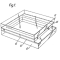
- a hermetically sealed envelope for a liquid crystal layer is formed by securing together two glass sheets 11 and 12 with a perimeter seal 13.
- the inward facing surfaces of the two sheets carry transparent electrode layers 14 and 15 of indium tin oxide, and each of these electrode layers is covered within the display area defined by the perimeter seal with a polymer layer, such as polyimide (not shown), provided for molecular alignment purposes.
- a polymer layer such as polyimide (not shown)
- Both polyimide layers are rubbed in a single direction so that when a lqiuid crystal is brought into contact with them they will tend to promote planar alignment of the liquid crystal molecules in the direction of the rubbing.
- the cell is assembled with the rubbing directions aligned parallel with each other.
- each one is patterned to define a set of strip electrodes (not shown) that individually extend across the display area and on out to beyond the perimeter seal to provide contact areas to which terminal connection may be made.
- the electrode strips of layer 14 extend transversely of those of layer 15 so as to define a pixel at each elemental area where an electrode strip of layer 15 is overlapped by a strip of layer 14.
- the thickness of the liquid crystal layer contained within the resulting envelope is determined by the thickness of the perimeter seal, and control over the precision of this may be provided by a light scattering of short lengths of glass fibre (not shown) of uniform diameter distributed through the material of the perimeter seal.
- the cell is filled by applying a vacuum to an aperture (not shown) through one of the glass sheets in one corner of the area enclosed by the perimeter seal so as to cause the liquid crystal medium to enter the cell by way of another aperture (not shown) located in the diagonally opposite corner. (Subsequent to the filling operation the two apertures are sealed.)
- the filling operation is carried out with the filling material heated into its isotropic phase so as to reduce its viscosity to a suitably low value.
- the basic construction of the cell is similar to that of for instance a conventional twisted nematic, except of course for the parallel alignment of the rubbing directions.
- the thickness of the perimeter seal 13, and hence of the liquid crystal layer is about 10 microns, but thinner or thicker layer thicknesses may be required to suit particular applications depending for instance upon whether or not bistability of operation is required and upon whether the layer is to be operated in the S* phase or in one of the more ordered phases such as SI or S F.
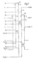
- Both types of data pulse 21a and 21b have a total duration of 4t s , starting t S before the beginning of the positive excursion of a strobe pulse, and ending t S after the end of its negative-going excursion.
- a data '1' pulse 21a commences by making a positive-going excursion to a voltage +V D for a duration t S , a negative-going excursion to a voltage -V D for a duration 2t s , and finally a positive-going excursion to +V D for a duration t S .
- a data '0' pulse 21b is the inverse of the data '0' pulse.
- the potential difference developed across the liquid crystal layer at a pixel addressed by the coincidence of a strobe pulse 20 with a data '1' pulse 21a is given by the pulse waveform 22a, while that of 22b is that which is produced at a pixel addressed by the coincidence of a strobe pulse 20 with a data '0' pulse 21b.
- the pixel is addressed by a voltage of duration t s and of magnitude IV s + V D
- V S and V D are chosen so that the pixel is appropriately switched by the
- the data employed to address the immediately preceding and immediately following lines may be such as to produce a pair of reverse polarity pulses of magnitude
- the strobe and data pulse waveforms allow individual pixels to be switched in either direction, that is data entry can be used to drive into the data '1' state selected pixels that were previously in the data '0' state, while at the same time other pixels that were previously in the '1' state are switched into the '0' state.
- the waveforms are charge balanced. These features are however attained at the expense of a line address time of 4t s even though the switching voltage magnitude
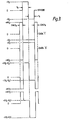
- FIG. 3 depicts waveforms according to one preferred embodiment of the present invention. Strobing, data '1' and data '0' pulse waveforms are depicted respectively at 30, 31a and 31b.
- the data pulse waveforms are applied in parallel to the electrode strips of one of the electrode layers 14, 15 while the strobe pulses are applied serially to those of the other electrode layer.
- a strobe pulse 30 is a balanced bipolar pulse having a negative-going voltage excursion to -V S following immediately after a positive-going one to +V S , both excursions being of duration t S .
- the data pulses 31a and 31b are also balanced bipolar pulses.
- a data '1' waveform includes a negative-going voltage excursion to -V D for a duration 2t S , which is both immediately preceded by, and immediately followed with, voltage excursions to +mV D for durations (1/m)t S , where 'm' is some factor greater than unity.
- a data '0' waveform is the voltage inverse of a data '1' waveform, and has a positive-going excursion to +V D for a duration 2t S , which is both immediately preceded by, and immediately followed with, voltage excursions to -mV D for durations (1/m)t S .
- the factor 'm' is the same for both data significances of data pulse, and in each case it is the voltage excursion of magnitude
Landscapes
- Engineering & Computer Science (AREA)
- Chemical & Material Sciences (AREA)
- Crystallography & Structural Chemistry (AREA)
- Physics & Mathematics (AREA)
- Computer Hardware Design (AREA)
- General Physics & Mathematics (AREA)
- Theoretical Computer Science (AREA)
- Liquid Crystal Display Device Control (AREA)
- Liquid Crystal (AREA)
Applications Claiming Priority (2)
| Application Number | Priority Date | Filing Date | Title |
|---|---|---|---|
| GB8508709 | 1985-04-03 | ||
| GB08508709A GB2173335B (en) | 1985-04-03 | 1985-04-03 | Addressing liquid crystal cells |
Publications (2)
| Publication Number | Publication Date |
|---|---|
| EP0196905A2 true EP0196905A2 (de) | 1986-10-08 |
| EP0196905A3 EP0196905A3 (de) | 1989-10-18 |
Family
ID=10577140
Family Applications (1)
| Application Number | Title | Priority Date | Filing Date |
|---|---|---|---|
| EP86302382A Ceased EP0196905A3 (de) | 1985-04-03 | 1986-04-01 | Flüssigkristall-Zellenadressierung |
Country Status (4)
| Country | Link |
|---|---|
| EP (1) | EP0196905A3 (de) |
| JP (1) | JPS61286818A (de) |
| AU (1) | AU580859B2 (de) |
| GB (1) | GB2173335B (de) |
Families Citing this family (8)
| Publication number | Priority date | Publication date | Assignee | Title |
|---|---|---|---|---|
| GB2173336B (en) * | 1985-04-03 | 1988-04-27 | Stc Plc | Addressing liquid crystal cells |
| GB2173337B (en) * | 1985-04-03 | 1989-01-11 | Stc Plc | Addressing liquid crystal cells |
| US5010328A (en) * | 1987-07-21 | 1991-04-23 | Thorn Emi Plc | Display device |
| GB8720856D0 (en) * | 1987-09-04 | 1987-10-14 | Emi Plc Thorn | Matrix addressing |
| GB2225473B (en) * | 1988-11-23 | 1993-01-13 | Stc Plc | Addressing scheme for multiplexded ferroelectric liquid crystal |
| DE69222959T2 (de) * | 1991-03-20 | 1998-03-19 | Seiko Epson Corp | Verfahren zum Betreiben einer Flüssigkristallanzeigevorrichtung vom Typ der aktiven Matrix |
| US6271817B1 (en) | 1991-03-20 | 2001-08-07 | Seiko Epson Corporation | Method of driving liquid crystal display device that reduces afterimages |
| GB9526270D0 (en) * | 1995-12-21 | 1996-02-21 | Secr Defence | Multiplex addressing of ferroelectric liquid crystal displays |
Family Cites Families (6)
| Publication number | Priority date | Publication date | Assignee | Title |
|---|---|---|---|---|
| FR2541807B1 (fr) * | 1983-02-24 | 1985-06-07 | Commissariat Energie Atomique | Procede de commande sequentielle d'un imageur matriciel utilisant l'effet de transition de phase cholesterique-nematique d'un cristal liquide |
| JPS6033535A (ja) * | 1983-08-04 | 1985-02-20 | Canon Inc | 液晶装置 |
| JPS6015624A (ja) * | 1983-07-08 | 1985-01-26 | Hitachi Ltd | 液晶プリンタの駆動方法 |
| GB2146473B (en) * | 1983-09-10 | 1987-03-11 | Standard Telephones Cables Ltd | Addressing liquid crystal displays |
| GB2173336B (en) * | 1985-04-03 | 1988-04-27 | Stc Plc | Addressing liquid crystal cells |
| GB2173337B (en) * | 1985-04-03 | 1989-01-11 | Stc Plc | Addressing liquid crystal cells |
-
1985
- 1985-04-03 GB GB08508709A patent/GB2173335B/en not_active Expired
-
1986
- 1986-03-27 AU AU55371/86A patent/AU580859B2/en not_active Ceased
- 1986-04-01 EP EP86302382A patent/EP0196905A3/de not_active Ceased
- 1986-04-03 JP JP7749586A patent/JPS61286818A/ja active Pending
Also Published As
| Publication number | Publication date |
|---|---|
| GB8508709D0 (en) | 1985-05-09 |
| GB2173335B (en) | 1988-02-17 |
| JPS61286818A (ja) | 1986-12-17 |
| EP0196905A3 (de) | 1989-10-18 |
| GB2173335A (en) | 1986-10-08 |
| AU580859B2 (en) | 1989-02-02 |
| AU5537186A (en) | 1986-10-09 |
Similar Documents
| Publication | Publication Date | Title |
|---|---|---|
| EP0197742B1 (de) | Flüssigkristall-Zellenadressierung | |
| EP0240222B1 (de) | Flüssigkristall-Zellenadressierung | |
| US4728947A (en) | Addressing liquid crystal cells using bipolar data strobe pulses | |
| EP0303343B1 (de) | Adressierung von Flüssigkristallzellen | |
| JPH0344284B2 (de) | ||
| US5216415A (en) | Method of driving a matrix-type liquid crystal display device | |
| US5047757A (en) | Method of addressing a ferroelectric liquid crystal display | |
| GB2173335A (en) | Addressing liquid crystal cells | |
| CA2002657C (en) | Addressing scheme for multiplexed ferro-electric liquid crystal | |
| KR100230092B1 (ko) | 액정셀의 어드레싱방법 | |
| JPH0679117B2 (ja) | 光学変調スイッチの駆動方法 | |
| JPS62253126A (ja) | 液晶素子の駆動方法 | |
| EP0549337A1 (de) | Flüssigkristallanzeigeeinrichtung | |
| JPH0448367B2 (de) | ||
| JPH0448366B2 (de) | ||
| JPH02126226A (ja) | 液晶電気光学素子 | |
| JPS6292921A (ja) | 光学変調スイツチの駆動方法 | |
| JPH0651280A (ja) | 強誘電性液晶素子の駆動方法 | |
| JPS61163325A (ja) | 液晶素子の駆動方法 | |
| JPH01179917A (ja) | 液晶素子の駆動方法 | |
| JPH0651279A (ja) | 強誘電性液晶素子の駆動方法 | |
| JPS63192020A (ja) | 強誘電性液晶電気光学装置 | |
| JPH0713519A (ja) | 強誘電性液晶装置の駆動方法 | |
| JPS63293530A (ja) | 液晶素子の駆動方法 | |
| JPS62272229A (ja) | 強誘電性液晶電気光学装置 |
Legal Events
| Date | Code | Title | Description |
|---|---|---|---|
| PUAI | Public reference made under article 153(3) epc to a published international application that has entered the european phase |
Free format text: ORIGINAL CODE: 0009012 |
|
| AK | Designated contracting states |
Kind code of ref document: A2 Designated state(s): DE FR IT |
|
| PUAL | Search report despatched |
Free format text: ORIGINAL CODE: 0009013 |
|
| AK | Designated contracting states |
Kind code of ref document: A3 Designated state(s): DE FR IT |
|
| 17P | Request for examination filed |
Effective date: 19900215 |
|
| RAP1 | Party data changed (applicant data changed or rights of an application transferred) |
Owner name: STC PLC |
|
| 17Q | First examination report despatched |
Effective date: 19910812 |
|
| RAP1 | Party data changed (applicant data changed or rights of an application transferred) |
Owner name: NORTHERN TELECOM LIMITED |
|
| STAA | Information on the status of an ep patent application or granted ep patent |
Free format text: STATUS: THE APPLICATION HAS BEEN REFUSED |
|
| 18R | Application refused |
Effective date: 19950530 |
|
| APAF | Appeal reference modified |
Free format text: ORIGINAL CODE: EPIDOSCREFNE |
|
| RIN1 | Information on inventor provided before grant (corrected) |
Inventor name: AYLIFFE, PETER JOHN Inventor name: DAVEY, ANTHONY BERNARD |