EP0197362A1 - Procédé utilisant un microscope à balayage pour déterminer les points sur un échantillon présentant un signal d'une fréquence prédéterminée - Google Patents
Procédé utilisant un microscope à balayage pour déterminer les points sur un échantillon présentant un signal d'une fréquence prédéterminée Download PDFInfo
- Publication number
- EP0197362A1 EP0197362A1 EP86103573A EP86103573A EP0197362A1 EP 0197362 A1 EP0197362 A1 EP 0197362A1 EP 86103573 A EP86103573 A EP 86103573A EP 86103573 A EP86103573 A EP 86103573A EP 0197362 A1 EP0197362 A1 EP 0197362A1
- Authority
- EP
- European Patent Office
- Prior art keywords
- evaluation circuit
- signal
- frequency
- scanning
- points
- Prior art date
- Legal status (The legal status is an assumption and is not a legal conclusion. Google has not performed a legal analysis and makes no representation as to the accuracy of the status listed.)
- Ceased
Links
- 238000000034 method Methods 0.000 title claims abstract description 23
- 238000011156 evaluation Methods 0.000 claims abstract description 60
- 238000010894 electron beam technology Methods 0.000 claims description 10
- 238000012876 topography Methods 0.000 claims description 3
- 238000013461 design Methods 0.000 claims description 2
- 230000001960 triggered effect Effects 0.000 claims 1
- 230000035945 sensitivity Effects 0.000 abstract description 7
- 238000011161 development Methods 0.000 description 5
- 238000005259 measurement Methods 0.000 description 3
- 239000000203 mixture Substances 0.000 description 2
- 230000003321 amplification Effects 0.000 description 1
- 230000002238 attenuated effect Effects 0.000 description 1
- 239000004020 conductor Substances 0.000 description 1
- 230000007423 decrease Effects 0.000 description 1
- 230000002542 deteriorative effect Effects 0.000 description 1
- 238000012986 modification Methods 0.000 description 1
- 230000004048 modification Effects 0.000 description 1
- 238000003199 nucleic acid amplification method Methods 0.000 description 1
- 230000003287 optical effect Effects 0.000 description 1
- 239000013307 optical fiber Substances 0.000 description 1
- 230000010355 oscillation Effects 0.000 description 1
- 230000000737 periodic effect Effects 0.000 description 1
- 230000002441 reversible effect Effects 0.000 description 1
- 238000005070 sampling Methods 0.000 description 1
- 238000004626 scanning electron microscopy Methods 0.000 description 1
- 238000012360 testing method Methods 0.000 description 1
Images

Classifications
-
- G—PHYSICS
- G01—MEASURING; TESTING
- G01R—MEASURING ELECTRIC VARIABLES; MEASURING MAGNETIC VARIABLES
- G01R31/00—Arrangements for testing electric properties; Arrangements for locating electric faults; Arrangements for electrical testing characterised by what is being tested not provided for elsewhere
- G01R31/28—Testing of electronic circuits, e.g. by signal tracer
- G01R31/302—Contactless testing
- G01R31/305—Contactless testing using electron beams
Definitions
- the invention relates to a method for determining the points on a sample carrying a signal of a specific signal frequency by means of a scanning microscope according to the generic terms of claims 1 and 3, and to circuit arrangements for carrying out the method.
- a method of this kind has been proposed in German patent application P 34 20 272.2.
- a corpuscular microscope is used in which a corpuscular beam, e.g. an electron beam, as the primary beam scans a group of points on a sample one after the other.
- the corpuscular beam is pulsed with an adjustable pulse frequency which deviates from the determined signal frequency by the amount of a fixed frequency, the first evaluation circuit consisting of a bandpass filter with a narrow pass band, the center frequency of which corresponds to the fixed frequency, and a subsequent demodulator.
- the maximum speed with which a group of points on the sample can be scanned in succession is limited by the bandwidth of the first evaluation circuit.
- this bandwidth must be as large as possible.
- the sensitivity of the method decreases with increasing bandwidth, since the signal-to-noise ratio of the output signal of the first evaluation circuit deteriorates. Therefore, in order to achieve a short measuring time, a reduction in the sensitivity or the spatial resolution of the scanned points on the sample must be accepted.
- the invention has for its object to bring about a reduction in the measurement time required for scanning the sample surface or a part thereof without deteriorating the spatial resolution and sensitivity. This is achieved according to the invention by designing the method mentioned at the outset according to the characterizing part of claim 1. According to a further invention, the object is also achieved with an embodiment of the method mentioned at the outset.
- the advantage that can be achieved with the invention is in particular that only those parts, for. B. conductor tracks, the sample surface that carry the signal frequency sought, are scanned at a relatively low speed and thus high sensitivity and spatial resolution, while the other parts are scanned at increased speed.
- the measurement time is therefore reduced considerably without the spatial resolution or the sensitivity of the method being reduced.
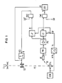
- the electrons emerging from an electron source 1 of a scanning electron microscope form a primary beam PE.
- This hits a point of a sample IC, for example an integrated circuit to be examined, and triggers secondary electrons SE there. These are detected in a detector DT.
- a detector DT Depending on the secondary electron current that strikes the detector DT, light pulses are generated in it, which are fed to a photomultiplier PM via an optical fiber 2 for emitting a secondary electrical signal.
- the secondary electrical signal is fed to input 3 of a first evaluation circuit LI, which is designed as a "lock-in" amplifier. That occurring at 4
- the output signal from LI goes to a comparator CM1, which is supplied with a comparably adjustable comparison voltage Uv1.
- the output signal from LI exceeds the value of Uv1, it is applied from the output of the comparator CM1 to the intensity control input 5 of a picture tube CRT.
- the electron beam of the picture tube is positioned via x and y deflection devices which are influenced via a (two-pole) input 6 by the deflection voltages generated by a raster generator G. Since G also influences the deflection systems for the primary beam PE indicated by SC1 with these deflection voltages, PE is deflected via a group of points on the sample IC, which corresponds to the deflection of the electron beam via the CRT screen via a group of assigned pixels.
- the integrated circuit IC is controlled by a control CON with a signal of the frequency n x fs.
- This signal is additionally fed to the first evaluation circuit LI via its input 7 as a reference voltage Ur via a frequency divider which divides n x fs into a frequency fs.
- the first evaluation circuit Li which is of narrow-band design, is tuned to the frequency fs by this reference voltage Ur. If the point sampled by PE now carries a signal of signal frequency fs, the secondary electrical signal derived via DT and PM, which is present at input 3 of LI, also contains a signal component with frequency fs. LI selects and demodulates this signal component, the output signal from LI controlling the intensity of the electron beam of the CRT.
- a second evaluation circuit LI ' is provided, which, however, is designed to be substantially broadband in accordance with the evaluation circuit LI.
- LI ' has its input at node 3 and is thus connected in parallel to the evaluation circuit LI on the input side. This also applies to the reference signal input from LI ', which is connected to node 7.
- the primary beam PE scans a group of points on the sample IC at a first scanning speed in accordance with the control of the deflection systems SC by means of the raster generator G.
- These points can lie, for example, on one line or on a multiplicity of parallel lines which cover the entire sample surface. If the point scanned in each case carries a signal with the frequency fs, an output signal is produced at the output 8 of the broadband evaluation circuit LI 'which is matched to fs via the reference voltage Ur, and which, when a threshold value given by Uv2 is exceeded, reaches the control input 9 of the raster generator G and the latter switches from the first scanning speed to a lower second scanning speed.
- An output signal is thus obtained at output 4 of LI, which is obtained at the lower, second sampling speed.
- This is used in the illustrated example for intensity modulation of the picture tube CRT so that the highlighted the signal frequency fs leading dots on the screen CRT by 'their brightness.
- the second evaluation circuit LI serves only to determine when a signal of the signal frequency fs is detected on the sample IC and to trigger the switch from G to the lower, second scanning speed when such a signal occurs.
- the first scanning speed can be selected so high that the areas of no interest on the sample IC which do not carry the signal of the signal frequency fs sought are quickly scanned.
- This high scanning speed which would not allow a precise determination of the signal-carrying points with a satisfactory spatial resolution and sensitivity at all, is achieved when the areas of interest on the sample in which the searched signal-carrying points are located are reached by a slow one, for the exact determination of these points necessary scanning speed replaced.
- the output signal from LI ' has then disappeared again, so that the raster generator G is switched back to the first, larger scanning speed.
- the signal frequency range of interest can be systematically searched by changing the frequency of the reference signal Ur.
- the bandwidth of the first evaluation circuit LI can be changed.
- it initially works in a broadband operating mode, the raster generator G being set to a first scanning speed.
- an input of LI is then controlled from there, via which the evaluation circuit is switched to its narrowband operating mode.
- the output 4 or 5 is also connected to the input 9 of G, so that G is switched to the lower, second scanning speed by the output signal at 4 or 5.
- the switching speed can be changed both in discrete steps and continuously. The further evaluation of the output signal from LI takes place in the manner already described.
- Ll can e.g. have a bandwidth of 100 Hz, Ll 'that of 1 kHz.
- the scanning electron microscope can e.g. consist of the ETEC Autoscan 11.
- a device of this type is known, for example, from US Pat. No. 4,277,679.
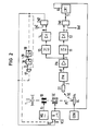
- FIG. 2 shows a further circuit arrangement which is suitable for carrying out the method according to the invention.
- a scanning electron microscope can be used here, e.g. is known from U.S. Patent 4,223,220.
- the circuit parts already described with reference to FIG. 1 are provided with the same reference symbols in FIG. 2.
- the intensity of the primary beam PE is modulated by means of a modulation system 10.
- a suitable modulation system is known, for example, from US Pat. No. 4,169,229. It is driven by a modulation generator MG with a modulation frequency fb which is offset by an amount df from the specific signal frequency fs that a sought point on the sample IC is to have.
- a signal of the signal frequency fs encountered on the sample mixes with the frequency fb with which PE is intensity modulated to an intermediate frequency signal of the fixed frequency df.
- the secondary electrical signal that is present at circuit point 3 thus has a signal component of the fixed frequency df.
- the first evaluation circuit here consists of a narrowband bandpass filter 11 and an amplitude demodulator 12 connected downstream of it.
- the second evaluation circuit is formed of a broadband bandpass filter 13 and an amplitude demodulator 14 connected downstream of this. Both band passes 11 and 13 are tuned to the frequency df.
- the signal component transmitted from the bandpass filter 11 to the output 4 is demodulated in 12, each signal exceeding Uv1 causing a brightness modulation of the respective pixel on the CRT.
- the secondary electrical signal is also selected via the broadband bandpass 13, demodulated in 14 and produces an output signal at the output 8, which is supplied to the control input 9 of G when a voltage threshold Uv2 is exceeded and to switch the latter from a first, relatively high scanning speed to a lower, second scanning speed.
- FIG. 3 shows a development of the arrangement according to FIG. 2, in which the intensity control input 5 of the picture tube CRT is fed to the output 4 of the first evaluation circuit 11, 12 in the illustrated position of a switch 15, as previously described. in this switching position 15 is only held during the occurrence of an output signal at the output 8 of the second evaluation circuit 13, 14. If there is no output signal at 8, a signal at terminal 16 is fed to input 5.
- This can e.g. are the output signal of the broadband evaluation circuit 13, 14 or a topography signal derived from the secondary electrical signal, which is supplied in particular in an attenuated form. How such a topography signal is obtained is e.g. from the book by L Reimer and G. Pfefferkorn): scanning electron microscopy (Springer-Verlag, Berlin, 2nd edition, 1977), pages 1-3 and 109-130.
- the output 8 of the second evaluation circuit 14 can also be connected to the first input of an OR gate 17, the output of which is then led to the control input 9 of G.
- output 8 is also connected to the clock input of a monoflop 18, the output 19 of which is connected to the clock input of a second monoflop 20, whose output 21 is connected to a second input of the OR gate 17.
- the output 19 is finally connected to a second one Control input 22 of G connected via which the scanning direction can be reversed when scanning the points on the sample IC.
- the monoflop 18 tilts and delivers a signal via 19 which causes a reversal of the scanning direction of the primary beam PE at the input 22 and also a reversal of the direction of travel of the electron beam of the CRT.
- the length of the signal emitted by 18 determines the extent of the return resulting for the primary beam PE and the electron beam from CRT. This return is expediently carried out at the high scanning speed.
- the second evaluation circuit 13, 14 can also be omitted if the bandwidth of the first evaluation circuit 11, 12 can be changed.
- the evaluation circuit 11, 12 initially works in a broadband operating mode, G being set to a first, relatively high scanning speed.
- G being set to a first, relatively high scanning speed.
- a control input of the bandpass 11, 12 is then assigned this signal, as a result of which a switchover from 11, 12 to the narrow-band operating mode takes place.
- the control input 9 of G is also assigned this signal, so that G is switched to the lower, second scanning speed.
- the switchover of the bandwidth and scanning speed can also be carried out here either in discrete steps or continuously.
- the output signals of the second evaluation circuit LI 'or 13, 14 obtained during a first fast scanning sequence can also be buffered, e.g. in the memory of a computer, with the aid of the first, narrow-band evaluation circuit LI or 11, 12 in a second slow scanning sequence in the areas in which output signals were obtained in the fast scanning sequence, an exact evaluation by the output signals of the first evaluation circuit is made.
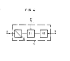
- FIG. 4 shows an expedient subcircuit of the raster generator G.
- This consists of a clock oscillator G1, the clock frequency of which is influenced by a signal applied to the input 9.
- G1 can also be called a VCO (Voltage Controlled Oscillator).
- a downstream counter Z1 counts the clock pulses emitted by G1, an analog signal corresponding in amplitude to the respective count result being derived via a digital-to-analog converter 23. With periodic resetting of Z1 to an initial value, this then represents a sawtooth-shaped deflection voltage which is output via output A.
- a signal is supplied to the input 22 which reverses the counting direction of Z1.
- the grid generator G expediently contains a circuit of the type shown in FIG. 4 for generating the x deflection voltage and the y deflection voltage.
- the reference voltage of the frequency fs can also be obtained in a different way than shown, e.g. from an output signal of the sample tC. This is recommended for integrated circuits with an internal clock oscillator that no longer require control.
- the difference frequency df can also be selected as the difference between fs or a multiple of fs and fb or a multiple of fb.
- the difference frequency df does not arise due to the mixture of the fundamental oscillations, but through a mixture with at least one harmonic. This can e.g. be advantageous if the modulation system has only a very limited bandwidth and you want to select higher-frequency signals fs.
- control CON is not absolutely necessary in the arrangements according to FIGS. 1 to 3, provided that the sample can also work without control.
- a synchronization of the reference signal Ur and the signal on the sample is also not absolutely necessary.
Landscapes
- Engineering & Computer Science (AREA)
- General Engineering & Computer Science (AREA)
- Physics & Mathematics (AREA)
- General Physics & Mathematics (AREA)
- Analysing Materials By The Use Of Radiation (AREA)
- Testing Of Individual Semiconductor Devices (AREA)
- Tests Of Electronic Circuits (AREA)
- Testing Or Measuring Of Semiconductors Or The Like (AREA)
Applications Claiming Priority (2)
| Application Number | Priority Date | Filing Date | Title |
|---|---|---|---|
| DE3510494 | 1985-03-22 | ||
| DE3510494 | 1985-03-22 |
Publications (1)
| Publication Number | Publication Date |
|---|---|
| EP0197362A1 true EP0197362A1 (fr) | 1986-10-15 |
Family
ID=6266084
Family Applications (1)
| Application Number | Title | Priority Date | Filing Date |
|---|---|---|---|
| EP86103573A Ceased EP0197362A1 (fr) | 1985-03-22 | 1986-03-17 | Procédé utilisant un microscope à balayage pour déterminer les points sur un échantillon présentant un signal d'une fréquence prédéterminée |
Country Status (3)
| Country | Link |
|---|---|
| US (1) | US4689555A (fr) |
| EP (1) | EP0197362A1 (fr) |
| JP (1) | JPS61225749A (fr) |
Cited By (2)
| Publication number | Priority date | Publication date | Assignee | Title |
|---|---|---|---|---|
| EP0226913A3 (fr) * | 1985-12-17 | 1988-10-05 | Siemens Aktiengesellschaft | Procédé et dispositif pour localiser et/ou afficher des points d'un échantillon conduisant un signal caractéristique dépendant du temps |
| US8076641B2 (en) | 2006-07-06 | 2011-12-13 | CarlZeiss NTS GmbH | Method and device for producing an image |
Families Citing this family (10)
| Publication number | Priority date | Publication date | Assignee | Title |
|---|---|---|---|---|
| EP0166814B1 (fr) * | 1984-05-30 | 1990-07-18 | Siemens Aktiengesellschaft | Méthode et dispositif pour détecter et afficher un point de mesure conduisant une tension d'au moins une certaine fréquence |
| EP0201692A1 (fr) * | 1985-03-22 | 1986-11-20 | Siemens Aktiengesellschaft | Procédé d'évaluation d'une tension de mesure à l'aide d'un circuit de traitement à bande poussante limitée et dispositif mettant en oeuvre ce procédé |
| JPH0646550B2 (ja) * | 1985-08-19 | 1994-06-15 | 株式会社東芝 | 電子ビ−ム定位置照射制御方法および電子ビ−ム定位置照射制御装置 |
| US4795976A (en) * | 1987-01-15 | 1989-01-03 | American Telephone And Telegraph Company At&T Bell Laboratories | Apparatus and derivative technique for testing devices |
| DE3887403D1 (de) * | 1987-08-06 | 1994-03-10 | Siemens Ag | Spannungsmessung mit einer Elektronensonde ohne externes Triggersignal. |
| US5685539A (en) * | 1995-07-05 | 1997-11-11 | Pitney Bowes Inc. | Disk transport for paper sheets |
| US6201240B1 (en) * | 1998-11-04 | 2001-03-13 | Applied Materials, Inc. | SEM image enhancement using narrow band detection and color assignment |
| JP4702472B2 (ja) * | 2009-07-28 | 2011-06-15 | 株式会社日立製作所 | 電子ビームを用いた検査方法及び検査装置 |
| JP4853581B2 (ja) * | 2010-08-11 | 2012-01-11 | 株式会社日立製作所 | 電子ビームを用いた検査方法及び検査装置 |
| US11610757B2 (en) * | 2019-08-28 | 2023-03-21 | Kla Corporation | Sensor module for scanning electron microscopy applications |
Citations (2)
| Publication number | Priority date | Publication date | Assignee | Title |
|---|---|---|---|---|
| DE2553705B1 (de) * | 1975-11-28 | 1977-03-31 | Siemens Ag | Schaltungsanordnung zur frequenzselektiven auswertung der amplituden eines oder mehrerer signale |
| US4420686A (en) * | 1981-01-29 | 1983-12-13 | Kabushiki Kaisha Akashi Seisakusho | Scanning electron microscope or similar equipment capable of displaying simultaneously a plurality of images of specimen |
Family Cites Families (3)
| Publication number | Priority date | Publication date | Assignee | Title |
|---|---|---|---|---|
| DE2743200A1 (de) * | 1977-09-26 | 1979-04-05 | Siemens Ag | Verbesserung an einer vorrichtung zur elektronenstrahleintastung |
| DE2813948A1 (de) * | 1978-03-31 | 1979-10-11 | Siemens Ag | Verfahren zur elektronischen abbildung der potentialverteilung in einem elektronischen bauelement |
| DE2903077C2 (de) * | 1979-01-26 | 1986-07-17 | Siemens AG, 1000 Berlin und 8000 München | Verfahren zur berührungslosen Potentialmessung an einem elektronischen Bauelement und Anordnung zur Durchführung des Verfahrens |
-
1986
- 1986-03-10 US US06/837,813 patent/US4689555A/en not_active Expired - Fee Related
- 1986-03-17 EP EP86103573A patent/EP0197362A1/fr not_active Ceased
- 1986-03-19 JP JP61061945A patent/JPS61225749A/ja active Pending
Patent Citations (2)
| Publication number | Priority date | Publication date | Assignee | Title |
|---|---|---|---|---|
| DE2553705B1 (de) * | 1975-11-28 | 1977-03-31 | Siemens Ag | Schaltungsanordnung zur frequenzselektiven auswertung der amplituden eines oder mehrerer signale |
| US4420686A (en) * | 1981-01-29 | 1983-12-13 | Kabushiki Kaisha Akashi Seisakusho | Scanning electron microscope or similar equipment capable of displaying simultaneously a plurality of images of specimen |
Non-Patent Citations (2)
| Title |
|---|
| ELECTRONICS INTERNATIONAL, Band 56, Nr. 10, 19. Mai 1983, Seiten 132-136, New York, US; H.-P. FEUERBAUM et al.: "Scanned electron-beam probe shows surface acoustic waves in action" * |
| IBM TECHNICAL DISCLOSURE BULLETIN, Band 15, Nr. 8, Januar 1973, Seiten 2547-2548, New York, US; J.J. DeSTAFENO et al.: "Display of voltage distributions on microcircuits" * |
Cited By (2)
| Publication number | Priority date | Publication date | Assignee | Title |
|---|---|---|---|---|
| EP0226913A3 (fr) * | 1985-12-17 | 1988-10-05 | Siemens Aktiengesellschaft | Procédé et dispositif pour localiser et/ou afficher des points d'un échantillon conduisant un signal caractéristique dépendant du temps |
| US8076641B2 (en) | 2006-07-06 | 2011-12-13 | CarlZeiss NTS GmbH | Method and device for producing an image |
Also Published As
| Publication number | Publication date |
|---|---|
| US4689555A (en) | 1987-08-25 |
| JPS61225749A (ja) | 1986-10-07 |
Similar Documents
| Publication | Publication Date | Title |
|---|---|---|
| DE2813948C2 (fr) | ||
| EP0428663B1 (fr) | Procede et dispositif d'analyse spectrale rapide de signaux en un ou plusieurs points de mesure | |
| DE3404611A1 (de) | Messsystem fuer kleine abmessungen mit hilfe eines abtastelektronenstrahls | |
| EP0166814B1 (fr) | Méthode et dispositif pour détecter et afficher un point de mesure conduisant une tension d'au moins une certaine fréquence | |
| DE2461202A1 (de) | Verfahren und vorrichtung zum automatischen fokussieren eines elektronenstrahls in einem abtastgeraet | |
| DE2605686C2 (de) | Verfahren und Vorrichtung zur graphischen Darstellung elektrischer Analogsignale | |
| DE3877827T2 (de) | Spannungsdetektor. | |
| DE2011470A1 (de) | Verfahren zum Auswerten eines nach einem Rasterverfahren aufgenommenen Bildes | |
| DE3045013C2 (fr) | ||
| DE2542356C2 (de) | Verfahren zur Fokussierung der Objektivlinse eines Korpuskular-Durchstrahlungs-Rastermikroskops und Einrichtung zur selbsttätigen Durchführung des Verfahrens, sowie Anwendung | |
| DE3614616C2 (fr) | ||
| DE2029627A1 (de) | Kompensationsschaltung für optische Abtasteinrichtung | |
| DE1801282C3 (de) | Schaltungsanordnung zur Ermittelung der Phasenlage, der Spannungsamplitude oder der Stromamplitude an beliebigen Stellen wiederholt auftretender elektrischer Meßsignale in bezug auf ein vorgegebenes Vergleichssignal | |
| EP0226913A2 (fr) | Procédé et dispositif pour localiser et/ou afficher des points d'un échantillon conduisant un signal caractéristique dépendant du temps | |
| EP0166815A1 (fr) | Méthode et dispositif pour l'analyse spectrale d'un signal en un point de mesure | |
| EP0169453A1 (fr) | Dispositif de circuit pour éviter les phénomènes de brûlure sur l'écran d'un indicateur visuel | |
| DE965908C (de) | Schaltung zur Regelspannungserzeugung, insbesondere in Fernsehempfaengern | |
| DE69020775T2 (de) | Detektor für ein optisches Signal. | |
| DE2141208A1 (de) | Vorrichtung zur Helligkeitssteuerung des Verlaufs von Vektoren auf dem Leuchtschirm einer Katodenstrahlröhre | |
| EP0201692A1 (fr) | Procédé d'évaluation d'une tension de mesure à l'aide d'un circuit de traitement à bande poussante limitée et dispositif mettant en oeuvre ce procédé | |
| EP0200893A1 (fr) | Méthode pour faire ressortir une partie de l'objet sur la surface d'un échantillon balayé par le faisceau primaire d'un microscope à balayage et dispositif pour sa mise en oeuvre | |
| DE2837981A1 (de) | Optisches zeitbereichs-reflektometer zur bestimmung der daempfung von lichtleitfasern | |
| DE2119850A1 (de) | Verfahren und Vorrichtung zum Darstellen eines Bilds und zum Messen eines darin befindlichen Objekts | |
| EP0196534A1 (fr) | Procédé pour déterminer les fréquences de signaux à au moins un point d'un échantillon à l'aide d'un microscope à balayage et dispositif mettant en oeuvre ce procédé | |
| EP0281795A1 (fr) | Procédé pour balayer un signal électrique variable dans le temps et dispositif pour sa mise en oeuvre et application d'un tel procédé |
Legal Events
| Date | Code | Title | Description |
|---|---|---|---|
| PUAI | Public reference made under article 153(3) epc to a published international application that has entered the european phase |
Free format text: ORIGINAL CODE: 0009012 |
|
| AK | Designated contracting states |
Kind code of ref document: A1 Designated state(s): DE FR GB IT NL |
|
| 17P | Request for examination filed |
Effective date: 19870408 |
|
| 17Q | First examination report despatched |
Effective date: 19900406 |
|
| STAA | Information on the status of an ep patent application or granted ep patent |
Free format text: STATUS: THE APPLICATION HAS BEEN REFUSED |
|
| 18R | Application refused |
Effective date: 19901001 |
|
| RIN1 | Information on inventor provided before grant (corrected) |
Inventor name: OTTO, JOHANN, DIPL.-ING. Inventor name: BRUST, HANS-DETLEF |