EP0226913A2 - Procédé et dispositif pour localiser et/ou afficher des points d'un échantillon conduisant un signal caractéristique dépendant du temps - Google Patents
Procédé et dispositif pour localiser et/ou afficher des points d'un échantillon conduisant un signal caractéristique dépendant du temps Download PDFInfo
- Publication number
- EP0226913A2 EP0226913A2 EP86116960A EP86116960A EP0226913A2 EP 0226913 A2 EP0226913 A2 EP 0226913A2 EP 86116960 A EP86116960 A EP 86116960A EP 86116960 A EP86116960 A EP 86116960A EP 0226913 A2 EP0226913 A2 EP 0226913A2
- Authority
- EP
- European Patent Office
- Prior art keywords
- signal
- arrangement
- frequency
- negation
- generated
- Prior art date
- Legal status (The legal status is an assumption and is not a legal conclusion. Google has not performed a legal analysis and makes no representation as to the accuracy of the status listed.)
- Withdrawn
Links
- 238000000034 method Methods 0.000 title claims abstract description 37
- 230000036962 time dependent Effects 0.000 title claims description 5
- 239000000523 sample Substances 0.000 title description 23
- 238000005259 measurement Methods 0.000 claims abstract description 10
- 238000013507 mapping Methods 0.000 claims abstract description 7
- 230000004807 localization Effects 0.000 claims abstract description 5
- 230000008859 change Effects 0.000 claims abstract description 4
- 238000011156 evaluation Methods 0.000 claims abstract 4
- 238000012876 topography Methods 0.000 claims description 13
- 238000012545 processing Methods 0.000 claims description 12
- 230000010354 integration Effects 0.000 claims description 6
- 238000003384 imaging method Methods 0.000 claims description 2
- 230000001960 triggered effect Effects 0.000 claims description 2
- 230000010363 phase shift Effects 0.000 claims 1
- 238000011144 upstream manufacturing Methods 0.000 claims 1
- 238000011161 development Methods 0.000 abstract description 4
- 238000004377 microelectronic Methods 0.000 abstract description 2
- 238000010894 electron beam technology Methods 0.000 description 19
- 239000004020 conductor Substances 0.000 description 10
- 239000000463 material Substances 0.000 description 7
- 230000008901 benefit Effects 0.000 description 4
- 238000012360 testing method Methods 0.000 description 4
- 230000004044 response Effects 0.000 description 3
- 238000009826 distribution Methods 0.000 description 2
- 230000006870 function Effects 0.000 description 2
- 238000011835 investigation Methods 0.000 description 2
- 230000007246 mechanism Effects 0.000 description 2
- 238000004364 calculation method Methods 0.000 description 1
- 230000002950 deficient Effects 0.000 description 1
- 230000003111 delayed effect Effects 0.000 description 1
- 230000001419 dependent effect Effects 0.000 description 1
- 230000000694 effects Effects 0.000 description 1
- 238000001914 filtration Methods 0.000 description 1
- 238000009499 grossing Methods 0.000 description 1
- 150000002500 ions Chemical class 0.000 description 1
- 238000004519 manufacturing process Methods 0.000 description 1
- 230000015654 memory Effects 0.000 description 1
- 238000012986 modification Methods 0.000 description 1
- 230000004048 modification Effects 0.000 description 1
- 239000013307 optical fiber Substances 0.000 description 1
- 230000000737 periodic effect Effects 0.000 description 1
- 230000008569 process Effects 0.000 description 1
- 230000002441 reversible effect Effects 0.000 description 1
- 238000007493 shaping process Methods 0.000 description 1
- 238000004088 simulation Methods 0.000 description 1
- 230000002123 temporal effect Effects 0.000 description 1
Images
Classifications
-
- G—PHYSICS
- G01—MEASURING; TESTING
- G01R—MEASURING ELECTRIC VARIABLES; MEASURING MAGNETIC VARIABLES
- G01R31/00—Arrangements for testing electric properties; Arrangements for locating electric faults; Arrangements for electrical testing characterised by what is being tested not provided for elsewhere
- G01R31/28—Testing of electronic circuits, e.g. by signal tracer
- G01R31/302—Contactless testing
- G01R31/305—Contactless testing using electron beams
Definitions
- the invention relates to a method for localizing and mapping the points of a sample carrying a specific time-dependent signal, and an arrangement for carrying out the method according to the preamble of claim 14.
- the present invention is based on the object of specifying a method and an arrangement of the type mentioned at the beginning, with the aid of which it is possible to check whether the expected signal caused by a periodic process occurring in the sample is present at a point of a sample to be examined , or in the case of defective samples, to determine whether a certain signal is still occurring. Furthermore, it should be ensured that the disturbing influence of the material and topography contrast is largely suppressed.
- the advantage that can be achieved with the invention is, in particular, that by suppressing the disruptive influence of the material and topography contrast, only the regions of the sample that carry the signal sought (for example conductor tracks of an integrated circuit) are imaged.
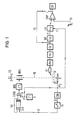
- a finely focused primary electron beam PE is generated in the electron-optical column of an electron beam measuring device known, for example, from US Pat. Nos. 4,220,853 or 4,223,220.
- This electron-optical column has, in addition to a large number of diaphragms and magnetic lens systems (not shown in FIGS. 1 and 2 for reasons of clarity) for beam shaping, beam deflection and beam focusing, an electron gun EG consisting essentially of a cathode, anode and Wehnelt electrode, and one over the beam blanking generator BBG controlled beam blanking system BBS.
- a detector DT made up of a suction network and a scintillator is provided, for example, to detect the secondary electrons SE triggered on the sample IC at the respectively selected point of impact of the primary electron beam PE.
- the detectable in the detector DT in its intensity at the individual measuring points due to the different potential, material and topography contrast fluctuating secondary electron current generates light pulses in the scintillator, which are fed to the photomultiplier PM via an optical fiber, and are converted here into a secondary electrical signal.
- the secondary electron signal generated in this way is then further amplified in a preamplifier PA, fed to a circuit SV for improving the signal-to-noise ratio (for example smoothing of the signal by low-pass filtering), and integrated in a downstream integrator INT over a specific time interval.
- the detector DT can also be preceded by a spectrometer SP, preferably an opposing field spectrometer, as is known, for example, from US Pat. No. 4,292,519, for measuring the shift in the energy distribution of the secondary electrons SE which is dependent on the sample potential.
- this spectrometer SP is indicated schematically by a flat counter-field electrode.
- An integrated circuit operating at nominal frequency is preferably provided as the sample IC, into which test programs adapted to the problem to be investigated are periodically fed via the control CON.
- characteristic signals defining the operating state then appear at nodes and conductor tracks during the test cycle, which signals can be compared to check the functionality with the signal profiles obtained, for example, from simulation calculations.
- the integrated circuit IC can of course be replaced by any sample which has conductive tracks or contact points at the points accessible for a primary electron beam PE.
- the method according to the invention allows the localization and mapping of the conductor tracks of an integrated circuit IC, which carry a specific, searched signal. Since the exemplary embodiment described below relates specifically to binary signals, the signal sought is then a specific bit pattern.
- the signal measured at the respectively selected measuring point of the sample IC is compared with the bit pattern sought using a correlation method.
- This correlation described below must be carried out for high-frequency signals (clock frequency> 5 MHz) because of the narrow bandwidth of the detector arrangement from the primary electron beam PE via the mechanism of the potential contrast.
- the amplitude or intensity of the primary electron current i PE is now modulated with the signal sought, for example by changing the primary electron beam PE according to the occurrence of time "HIGH and" LOW "values of the bit pattern g (t) sought and keyed in, and at the same time integrating the secondary electron current i SE measured in the detector DT, the correlation defined in equation 1) is being carried out.
- the non-linearity of the potential contrast characteristic interferes not in this context, since only binary signals g (t) and f (t) are present.
- the primary electron beam PE is, according to the invention, alternately modulated with the bit pattern g (t) sought and its negation, ie as a function of the "HIGH” and - occurring in the respective bit sequence "LOW" values are keyed in and out using the BBS beam blanking system.
- the bit pattern sought is read into the shift register SR before the start of the measurement, the content of which is shifted cyclically during the measurement with a frequency f 2 predetermined by the external clock signal CLK.
- the clock signal CLK can be obtained, for example, from the clock frequency nf2 generated by the control CON by frequency division.
- the output signal of the shift register SR corresponding to the bit pattern being sought is either negated or not negated via the EXOR gate to the beam blanking generator BBG controlling the beam blanking system BBS.
- the beam blanking system BBS can also be controlled directly via the amplified output signal of the EXOR gate.
- the integrator INT supplies an output signal whose amplitude changes with the switching frequency f 1 between the extreme values c min and c max defined by equations 3) and 4).
- the fluctuation amplitude ⁇ c: c max - c min 5) is therefore always at a maximum if the conductor track in question leads the bit pattern sought.
- the fluctuation of the output signal generated by the integrator INT is always smaller than the variable c defined in equation 5).
- This also applies in particular to the areas of the sample IC in which, due to special materials (oxide layers) or the topography (edges), particularly many or a few secondary electrons SE are emitted and detected in the detector DT. Since the secondary electron signal determined in these areas essentially by the material or topography contrast and integrated in the integrator INT remains largely constant, regardless of the negated or non-negated bit pattern modulating the primary electron beam PE, the fluctuation of the integrator output signal is also less than in this case c.
- the integrator INT is followed by a lock-in amplifier LIV, the reference input RE of which is connected to the output of the signal generator G.
- a phase-sensitive detector LIV for example, a bandpass filter tuned to the switching frequency f 1 with a downstream amplitude demodulator (for example, a peak value rectifier can be used).
- the fluctuation amplitude is compared with the variable response threshold TH in the comparator CMP, the positive input of which is connected to the output signal of the lock-in amplifier LIV.
- the comparator CMP always only generates then a signal when the fluctuation of the integrator output signal lies above the response threshold TH, that is to say whenever the respective measuring point leads the bit pattern sought in phase.
- an integrator as an independent component can be dispensed with entirely, since for high frequencies the detector DT and for low frequencies with a suitable choice of the scanning speed the CRT of the scanning electron microscope itself have an integrating effect.
- the conductor tracks of the sample IC that carry a specific bit pattern their surface is scanned line by line or point by point with the primary electron beam PE. This scanning must take place so slowly that the correlation method described above is actually carried out at every point on the surface within the time interval in which the expected signal can occur.
- the primary corpuscular beam must therefore remain positioned at every measuring point at least during the integration period. If this is not the case, the measurement can be carried out periodically.
- the output signal of the comparator CMP is recorded as a function of the measuring point which is respectively acted upon by the primary electron beam PE.
- a simple recording possibility is to use the output signal of the comparator CMP to modulate the intensity of the write beam of the picture tube CRT, which is deflected synchronously with the primary electron beam PE, so that all conductor tracks which carry the signal sought are displayed brightly.
- Output signal of the comparator CMP superimpose a topography signal (for example the conventional secondary electron image of the sample IC) and display it at the same time. In Fig. 1, this is indicated schematically by the signal line TS.
- the phase at which the check is carried out can be set via the delay element DL. Since only the phase difference is of interest, the delay element DL can of course also be arranged between the control CON and probe IC.
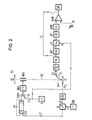
- An arrangement according to the invention with which this check can be carried out in a phase-independent manner and with which it can thus be tested whether the expected bit pattern is present at the measuring point at all is shown in FIG. 2, in the same reference numerals the same arrangement elements already described in connection with FIG. 1 describe.
- the electrically controllable delay element DL is driven by a generator GDL with the frequency f3, so that with the delay time the phase position of the primary electron beam PE modulated with the bit pattern sought or with its negation periodically with the frequency relative to the signal present at the measuring point f3 changes.
- the output signal of the integrator INT in addition to the signal component generated by switching the EXOR gate with the frequency f 1 also a signal component with the generally lower frequency f 3 if the measuring point leads the bit pattern sought.
- the signal component with the frequency f 1 can be filtered out again with the aid of a phase-sensitive detector, so that a LIV at the output of the lock-in amplifier shown in FIG Signal of frequency f3 can be tapped, which is fed to the input of the bandpass filter BP tuned to this frequency.
- the amplitude of this signal of frequency f3 is then determined in the downstream amplitude demodulator AMD, and compared in the comparator CMP with the variable response threshold TH, the comparator output signal depending on the location of the measuring point on the sample IC being recorded again or for controlling the intensity of the CRT can be used.
- the amplitude demodulator AMD is of course also superfluous.
- the frequency f 1 with which the EXOR gate is switched also less than the frequency f 3 with which the delay element DL is driven. In this case, however, you must first filter out the frequency f3 and then only the frequency f1 from the secondary electron signal, since the frequency f1 now appears as a modulation on the frequency f3 now acting as the carrier frequency.
- the lock-in amplifier LIV and the bandpass filter BP with a downstream amplitude demodulator AMD then appear in reverse order within the signal chain.
- a change in the phase position of the primary electron beam PE modulated with the bit pattern or its negation relative to the signal present at the measuring point can also be achieved simply by changing the frequency f 2 with which the bit sequence in the shift register SR is shifted cyclically, and by the Control CON generated clock frequency slightly offset from each other.
- the signal that can then be tapped at the output of the lock-in amplifier LIV with the predetermined differential frequency can again be fed to a bandpass filter tuned to this frequency.
- the upper limit frequency is determined by the beam blanking system BBS used. Since beam blanking systems BBS which are already operating in the GHz range are currently available, the arrangements according to the invention can be used to check integrated circuits IC under real operating conditions.
- the secondary electron current i SE that is alternately modulated with the bit pattern sought or its negation.
- a secondary electron spectrometer SP as is known, for example, from US Pat. No. 4,292,419, can be used as the modulator, in which the signal or bit pattern or its negation sought is the height of the potential wall built up in the spectrometer SP and thus also the intensity controls the secondary electron current i SE detectable in the detector DT.
- the output signal of the EXOR gate in a modification of the arrangements shown in FIGS.
- the advantage of this method is, in particular, that no BBS beam blanking system is required.
- the limit frequency that can be achieved with such an arrangement is, however, due to the relatively high capacity of the spectrometer SP, lower than that of the arrangements according to FIGS. 1 and 2.
- a detector DT can also be used to modulate the secondary electron current i SE . or bit pattern is controlled.
- the output signal of the EXOR gate is advantageously fed to an input of an adder, the output of which is in turn connected to the suction electrode of the detector DT. Otherwise the electrode for signal processing shown in FIGS. 1 and 2 remains unchanged.
- the secondary electron signal generated in signal processing (for example a detector-photomultiplier-amplifier arrangement) is modulated with the desired signal or bit pattern, for example with the aid of a gate circuit.
- the beam blanking system BBS and the associated signal generator BBG an arrangement for carrying out this method has all the circuit elements shown in FIGS. 1 and 2 and additionally a mixer arranged, for example, between the circuit SV for improving the signal-to-noise ratio and the integrator INT on. A second input of this mixer is in turn connected to the output of the EXOR gate.
- a multiplier can be used for the sought analog signal, for example a simple electronic switch for sought digital signals (bit patterns).
- This identification can be used to filter out the associated fluctuation amplitude from the processed secondary electron signal with the aid of a suitable filter or demodulator.
- a simple way of implementing this is, for example, to control the input B of the EXOR gate via a random bit sequence generator (a so-called pn or p seudo n oise generator) in the arrangement shown in FIG. 1 and the fluctuation amplitude of interest with the aid of a Filter out the random bit sequence of coordinated correlators.
- the secondary electron signal measured at every point of the sample IC does not have to arise exclusively through potential contrast.
- Any other contrast mechanism in which the secondary electrons SE are influenced by a signal present at the measuring point is suitable for this.
- the secondary electrons SE are deflected by local magnetic fields when using magnetic bubble memories as a sample IC (magnetic contrast).
- the invention is of course not limited to the use of electrons as primary and secondary corpuscles.
- ions or other corpuscles can also be considered as primary or secondary corpuscles.
- Lasers can of course also be used to generate a primary beam.
Landscapes
- Engineering & Computer Science (AREA)
- General Engineering & Computer Science (AREA)
- Physics & Mathematics (AREA)
- General Physics & Mathematics (AREA)
- Testing Or Measuring Of Semiconductors Or The Like (AREA)
- Tests Of Electronic Circuits (AREA)
- Testing Of Individual Semiconductor Devices (AREA)
Applications Claiming Priority (2)
| Application Number | Priority Date | Filing Date | Title |
|---|---|---|---|
| DE3544600 | 1985-12-17 | ||
| DE3544600 | 1985-12-17 |
Publications (2)
| Publication Number | Publication Date |
|---|---|
| EP0226913A2 true EP0226913A2 (fr) | 1987-07-01 |
| EP0226913A3 EP0226913A3 (fr) | 1988-10-05 |
Family
ID=6288654
Family Applications (1)
| Application Number | Title | Priority Date | Filing Date |
|---|---|---|---|
| EP86116960A Withdrawn EP0226913A3 (fr) | 1985-12-17 | 1986-12-05 | Procédé et dispositif pour localiser et/ou afficher des points d'un échantillon conduisant un signal caractéristique dépendant du temps |
Country Status (4)
| Country | Link |
|---|---|
| US (1) | US4820977A (fr) |
| EP (1) | EP0226913A3 (fr) |
| JP (1) | JPS62156829A (fr) |
| CA (1) | CA1254670A (fr) |
Families Citing this family (10)
| Publication number | Priority date | Publication date | Assignee | Title |
|---|---|---|---|---|
| JPS6435838A (en) * | 1987-07-31 | 1989-02-06 | Jeol Ltd | Charged particle beam device |
| NL8802335A (nl) * | 1988-09-21 | 1990-04-17 | Philips Nv | Werkwijze en inrichting voor het op sub-mikron schaal bewerken van een materiaal-oppervlak. |
| DE3917411A1 (de) * | 1989-05-29 | 1990-12-06 | Brust Hans Detlef | Verfahren und anordnung zur schnellen spektralanalyse eines signals an einem oder mehreren messpunkten |
| EP0504944B1 (fr) * | 1991-03-22 | 1998-09-23 | Nec Corporation | Procédé d'analyse de fautes utilisant un faisceau d'électrons |
| JP2685425B2 (ja) * | 1994-09-30 | 1997-12-03 | 株式会社東芝 | 液晶素子評価方法 |
| US5638005A (en) * | 1995-06-08 | 1997-06-10 | Schlumberger Technologies Inc. | Predictive waveform acquisition |
| US6466040B1 (en) * | 1997-08-01 | 2002-10-15 | Carl Zeiss Jena Gmbh | Three dimensional optical beam induced current (3-D-OBIC) |
| FR2841418A1 (fr) * | 2002-06-20 | 2003-12-26 | Thomson Licensing Sa | Dispositif numerique de correction de l'image formee sur l'ecran d'un tube a rayons cathodiques |
| US8754633B2 (en) | 2009-05-01 | 2014-06-17 | Dcg Systems, Inc. | Systems and method for laser voltage imaging state mapping |
| DE112014000306B4 (de) * | 2013-01-31 | 2020-03-26 | Hitachi High-Technologies Corporation | Kombinierte Ladungsteilchenstrahlvorrichtung |
Family Cites Families (16)
| Publication number | Priority date | Publication date | Assignee | Title |
|---|---|---|---|---|
| DE2813948A1 (de) * | 1978-03-31 | 1979-10-11 | Siemens Ag | Verfahren zur elektronischen abbildung der potentialverteilung in einem elektronischen bauelement |
| DE2814049A1 (de) * | 1978-03-31 | 1979-10-18 | Siemens Ag | Verfahren zur beruehrungslosen messung des potentialverlaufs in einem elektronischen bauelement und anordnung zur durchfuehrung des verfahrens |
| JPS5571024A (en) * | 1978-11-24 | 1980-05-28 | Hitachi Ltd | Mark sensing method |
| DE2902495A1 (de) * | 1979-01-23 | 1980-07-31 | Siemens Ag | Einrichtung zur beruehrungslosen potentialmessung |
| DE2903077C2 (de) * | 1979-01-26 | 1986-07-17 | Siemens AG, 1000 Berlin und 8000 München | Verfahren zur berührungslosen Potentialmessung an einem elektronischen Bauelement und Anordnung zur Durchführung des Verfahrens |
| DE3036708A1 (de) * | 1980-09-29 | 1982-05-13 | Siemens AG, 1000 Berlin und 8000 München | Elektronenstrahl-messgeraet zur stroboskopischen messung hochfrequenter periodischer vorgaenge |
| DE3036660A1 (de) * | 1980-09-29 | 1982-05-19 | Siemens AG, 1000 Berlin und 8000 München | Anordnung fuer stroboskopische potentialmessungen mit einem elektronenstrahl-messgeraet |
| JPS5931549A (ja) * | 1982-08-13 | 1984-02-20 | Hitachi Ltd | ストロボ走査形電子顕微鏡の像表示装置 |
| JPS59141238A (ja) * | 1983-02-01 | 1984-08-13 | Hitachi Ltd | キヤリア寿命測定装置 |
| JPS6070651A (ja) * | 1983-09-28 | 1985-04-22 | Hitachi Ltd | 焦点合わせ方法およびその装置 |
| DE3407041A1 (de) * | 1984-02-27 | 1985-09-05 | Siemens AG, 1000 Berlin und 8000 München | Verfahren zur automatischen einstellung des arbeitspunktes bei signalverlaufsmessungen mit korpuskularstrahl-messgeraeten |
| DE3407071A1 (de) * | 1984-02-27 | 1985-08-29 | Siemens AG, 1000 Berlin und 8000 München | Verfahren zur automatischen einstellung der spannungsaufloesung in korpuskularstrahl-messgeraeten und vorrichtung zur durchfuehrung eines solchen verfahrens |
| DE3482769D1 (de) * | 1984-05-30 | 1990-08-23 | Siemens Ag | Verfahren und vorrichtung zur detektion und abbildung eines messpunkts, der eine spannung wenigstens einer bestimmten frequenz fuehrt. |
| DE3428965A1 (de) * | 1984-08-06 | 1986-02-06 | Siemens AG, 1000 Berlin und 8000 München | Verfahren und vorrichtung zur detektion und abbildung von messpunkten, die einen bestimmten signalverlauf aufweisen |
| US4864228A (en) * | 1985-03-15 | 1989-09-05 | Fairchild Camera And Instrument Corporation | Electron beam test probe for integrated circuit testing |
| US4689555A (en) * | 1985-03-22 | 1987-08-25 | Siemens Aktiengesellschaft | Method for the determination of points on a specimen carrying a specific signal frequency by use of a scanning microscope |
-
1986
- 1986-12-05 EP EP86116960A patent/EP0226913A3/fr not_active Withdrawn
- 1986-12-15 US US06/941,646 patent/US4820977A/en not_active Expired - Fee Related
- 1986-12-15 CA CA000525271A patent/CA1254670A/fr not_active Expired
- 1986-12-16 JP JP61301099A patent/JPS62156829A/ja active Pending
Also Published As
| Publication number | Publication date |
|---|---|
| US4820977A (en) | 1989-04-11 |
| CA1254670A (fr) | 1989-05-23 |
| JPS62156829A (ja) | 1987-07-11 |
| EP0226913A3 (fr) | 1988-10-05 |
Similar Documents
| Publication | Publication Date | Title |
|---|---|---|
| EP0189777B1 (fr) | Méthode de mesure par faisceau de particules pour le test sans contact de circuits | |
| DE2813948C2 (fr) | ||
| DE2814049C2 (fr) | ||
| EP0428663B1 (fr) | Procede et dispositif d'analyse spectrale rapide de signaux en un ou plusieurs points de mesure | |
| DE68914178T2 (de) | Elektroumstrahlprüfung von elektronischen Komponenten. | |
| DE2005682C3 (de) | Vorrichtung zum Absaugen der Sekundärelektronen in einem Rasterelektronenmikroskop oder einem Elektronenstrahl-Mikroanalysator | |
| DE2813947A1 (de) | Verfahren zur beruehrungslosen messung des potentialverlaufs in einem elektronischen bauelement und anordnung zur durchfuehrung des verfahrens | |
| EP0166814B1 (fr) | Méthode et dispositif pour détecter et afficher un point de mesure conduisant une tension d'au moins une certaine fréquence | |
| DE1943140B2 (de) | Verfahren zum analysieren des oberflaechenpotentials eines prueflings | |
| EP0013876A1 (fr) | Appareil pour mesurer sans contact un potentiel | |
| EP0172470B1 (fr) | Procédé et dispositif pour détecter et représenter des points de mesure correspondant à un signal de forme spécifique | |
| EP0196531B1 (fr) | Procédé pour déterminer indirectement la distribution de l'intensité d'impulsions de faisceaux de particules créés dans un appareil de mesure à faisceau de particules | |
| EP0285896A2 (fr) | Procédé pour l'essai des réseaux de lignes | |
| EP1801844A2 (fr) | Procédé et dispositif pour mesurer de la distance | |
| EP0310816B1 (fr) | Poursuite automatique de fréquence dans un procédé mesureur de rayons corpusculaires utilisant un rayon primaire modulé | |
| EP0166815A1 (fr) | Méthode et dispositif pour l'analyse spectrale d'un signal en un point de mesure | |
| EP0232790A1 (fr) | Procédé et dispositif pour mesurer des signaux en fonction du temps avec une sonde à rayon corpusculaire | |
| DE1946931A1 (de) | Verfahren zum Pruefen von Schaltungen und Vorrichtung zur Ausfuehrung des Verfahrens | |
| EP0302241A2 (fr) | Mesure de tension avec une sonde à électrons sans signal de déclenchement externe | |
| DE69900869T2 (de) | Verfahren und Vorrichtung zur Prüfung eines elektronischen Bauteils | |
| EP0395679B1 (fr) | Procede et dispositif de mesure de la variation dans le temps de signaux a la pointe de mesure d'un specimen | |
| EP0301254A2 (fr) | Mesure de tension utilisant une sonde à électrons en mesurant dans le domaine des fréquences à l'aide d'un rayon primaire modulé | |
| DE4002531A1 (de) | Verfahren und anordnung zur spektralanalyse eines signals | |
| DE3519401A1 (de) | Verfahren und vorrichtung zur detektion und abbildung eines punktes einer probe, der ein signal wenigstens einer bestimmten frequenz fuehrt | |
| DE3941178A1 (de) | Verfahren zur quantitativen potentialmessung mit einer korpuskularsonde |
Legal Events
| Date | Code | Title | Description |
|---|---|---|---|
| PUAI | Public reference made under article 153(3) epc to a published international application that has entered the european phase |
Free format text: ORIGINAL CODE: 0009012 |
|
| AK | Designated contracting states |
Kind code of ref document: A2 Designated state(s): AT BE CH DE FR GB IT LI LU NL SE |
|
| PUAL | Search report despatched |
Free format text: ORIGINAL CODE: 0009013 |
|
| AK | Designated contracting states |
Kind code of ref document: A3 Designated state(s): AT BE CH DE FR GB IT LI LU NL SE |
|
| 17P | Request for examination filed |
Effective date: 19890330 |
|
| 17Q | First examination report despatched |
Effective date: 19901017 |
|
| STAA | Information on the status of an ep patent application or granted ep patent |
Free format text: STATUS: THE APPLICATION IS DEEMED TO BE WITHDRAWN |
|
| 18D | Application deemed to be withdrawn |
Effective date: 19910228 |
|
| RIN1 | Information on inventor provided before grant (corrected) |
Inventor name: BRUST, HANS-DETLEF |