EP0197738B1 - Méthode de fabrication d'un dispositif semiconducteur de type LDD - Google Patents
Méthode de fabrication d'un dispositif semiconducteur de type LDD Download PDFInfo
- Publication number
- EP0197738B1 EP0197738B1 EP86302357A EP86302357A EP0197738B1 EP 0197738 B1 EP0197738 B1 EP 0197738B1 EP 86302357 A EP86302357 A EP 86302357A EP 86302357 A EP86302357 A EP 86302357A EP 0197738 B1 EP0197738 B1 EP 0197738B1
- Authority
- EP
- European Patent Office
- Prior art keywords
- layer
- conductive layer
- gate electrode
- semiconductor device
- manufacturing
- Prior art date
- Legal status (The legal status is an assumption and is not a legal conclusion. Google has not performed a legal analysis and makes no representation as to the accuracy of the status listed.)
- Expired - Lifetime
Links
Images
Classifications
-
- H—ELECTRICITY
- H10—SEMICONDUCTOR DEVICES; ELECTRIC SOLID-STATE DEVICES NOT OTHERWISE PROVIDED FOR
- H10D—INORGANIC ELECTRIC SEMICONDUCTOR DEVICES
- H10D30/00—Field-effect transistors [FET]
- H10D30/60—Insulated-gate field-effect transistors [IGFET]
- H10D30/601—Insulated-gate field-effect transistors [IGFET] having lightly-doped drain or source extensions, e.g. LDD IGFETs or DDD IGFETs
-
- H—ELECTRICITY
- H10—SEMICONDUCTOR DEVICES; ELECTRIC SOLID-STATE DEVICES NOT OTHERWISE PROVIDED FOR
- H10P—GENERIC PROCESSES OR APPARATUS FOR THE MANUFACTURE OR TREATMENT OF DEVICES COVERED BY CLASS H10
- H10P95/00—Generic processes or apparatus for manufacture or treatments not covered by the other groups of this subclass
-
- H—ELECTRICITY
- H10—SEMICONDUCTOR DEVICES; ELECTRIC SOLID-STATE DEVICES NOT OTHERWISE PROVIDED FOR
- H10D—INORGANIC ELECTRIC SEMICONDUCTOR DEVICES
- H10D30/00—Field-effect transistors [FET]
- H10D30/01—Manufacture or treatment
- H10D30/021—Manufacture or treatment of FETs having insulated gates [IGFET]
- H10D30/0223—Manufacture or treatment of FETs having insulated gates [IGFET] having source and drain regions or source and drain extensions self-aligned to sides of the gate
- H10D30/0227—Manufacture or treatment of FETs having insulated gates [IGFET] having source and drain regions or source and drain extensions self-aligned to sides of the gate having both lightly-doped source and drain extensions and source and drain regions self-aligned to the sides of the gate, e.g. lightly-doped drain [LDD] MOSFET or double-diffused drain [DDD] MOSFET
-
- H—ELECTRICITY
- H10—SEMICONDUCTOR DEVICES; ELECTRIC SOLID-STATE DEVICES NOT OTHERWISE PROVIDED FOR
- H10D—INORGANIC ELECTRIC SEMICONDUCTOR DEVICES
- H10D30/00—Field-effect transistors [FET]
- H10D30/60—Insulated-gate field-effect transistors [IGFET]
-
- H—ELECTRICITY
- H10—SEMICONDUCTOR DEVICES; ELECTRIC SOLID-STATE DEVICES NOT OTHERWISE PROVIDED FOR
- H10D—INORGANIC ELECTRIC SEMICONDUCTOR DEVICES
- H10D64/00—Electrodes of devices having potential barriers
- H10D64/60—Electrodes characterised by their materials
- H10D64/66—Electrodes having a conductor capacitively coupled to a semiconductor by an insulator, e.g. MIS electrodes
- H10D64/661—Electrodes having a conductor capacitively coupled to a semiconductor by an insulator, e.g. MIS electrodes the conductor comprising a layer of silicon contacting the insulator, e.g. polysilicon having vertical doping variation
- H10D64/662—Electrodes having a conductor capacitively coupled to a semiconductor by an insulator, e.g. MIS electrodes the conductor comprising a layer of silicon contacting the insulator, e.g. polysilicon having vertical doping variation the conductor further comprising additional layers, e.g. multiple silicon layers having different crystal structures
-
- H—ELECTRICITY
- H10—SEMICONDUCTOR DEVICES; ELECTRIC SOLID-STATE DEVICES NOT OTHERWISE PROVIDED FOR
- H10D—INORGANIC ELECTRIC SEMICONDUCTOR DEVICES
- H10D64/00—Electrodes of devices having potential barriers
- H10D64/60—Electrodes characterised by their materials
- H10D64/66—Electrodes having a conductor capacitively coupled to a semiconductor by an insulator, e.g. MIS electrodes
- H10D64/661—Electrodes having a conductor capacitively coupled to a semiconductor by an insulator, e.g. MIS electrodes the conductor comprising a layer of silicon contacting the insulator, e.g. polysilicon having vertical doping variation
- H10D64/662—Electrodes having a conductor capacitively coupled to a semiconductor by an insulator, e.g. MIS electrodes the conductor comprising a layer of silicon contacting the insulator, e.g. polysilicon having vertical doping variation the conductor further comprising additional layers, e.g. multiple silicon layers having different crystal structures
- H10D64/663—Electrodes having a conductor capacitively coupled to a semiconductor by an insulator, e.g. MIS electrodes the conductor comprising a layer of silicon contacting the insulator, e.g. polysilicon having vertical doping variation the conductor further comprising additional layers, e.g. multiple silicon layers having different crystal structures the additional layers comprising a silicide layer contacting the layer of silicon, e.g. polycide gates
-
- H—ELECTRICITY
- H10—SEMICONDUCTOR DEVICES; ELECTRIC SOLID-STATE DEVICES NOT OTHERWISE PROVIDED FOR
- H10P—GENERIC PROCESSES OR APPARATUS FOR THE MANUFACTURE OR TREATMENT OF DEVICES COVERED BY CLASS H10
- H10P14/00—Formation of materials, e.g. in the shape of layers or pillars
- H10P14/40—Formation of materials, e.g. in the shape of layers or pillars of conductive or resistive materials
- H10P14/412—Deposition of metallic or metal-silicide materials
Definitions
- This invention relates to a method for manufacturing a semiconductor device, and in particular relates to a metal oxide silicon (MOS) transistor having a lightly doped drain (LDD) structure.
- MOS metal oxide silicon
- LDD lightly doped drain
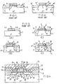
- a well-known n channel MOS transistor is shown in Figure 1 and is fabricated as follows. First, a thermal oxide layer 4 is formed on a p-type silicon substrate 1. Then channel region 2 is provided on silicon substrate 1 by implantation of impurity ions such as boron (B), for controlling the short channel effect of the threshold voltage. After a gate electrode 3 is formed on the thermal oxide layer 4, the thermal oxide layer 4 is selectively removed by an etching technique using the gate electrode 3 as a mask and a gate oxide film 4 is formed. An n + type source region 5 and a drain region 6 are formed by implantation of impurity ions, for example, arsenic (As), in the silicon substrate 1 using the gate electrode 3 as a mask.
- impurity ions such as boron (B)
- the LDD structure MOS transistor has been developed for reducing the above-mentioned problems.
- a lightly doped impurity source region 7 and drain region 8 are formed in the vicinity of gate electrode 3.
- This structure reduces the strength of the high electric field set up in the vicinity of the drain region, because the impurity concentration of source region 7 and drain region 8 is lower than that of source region 5 and drain region 6. As a consequence, electrons are not injected into the gate insulation layer.
- This LDD structure MOS transistor is typically manufactured according to the process shown in Figure 3.
- a gate oxide layer 4 and a gate electrode 3 are formed on the silicon substrate 1
- phosphorus (P) or arsenic (As) for example, is introduced by ion implantation in a light dope using the gate electrode as a mask (see Figure 3A).
- a source region 7 and a drain region 8 are then activated by heat treatment and an oxide layer 9 of 3000 Angstrom units thickness is deposited using a low temperature (400°C-500°C) and an atmospheric pressure chemical vapor deposition method (APCVD), as shown in Figure 3B.
- APCVD atmospheric pressure chemical vapor deposition method
- the oxide layer is anisotropically etched by the reactive ion etching (RIE) method and a side-wall spacer 10 of oxide layer 9 is formed on the lateral face of the gate electrode 3, as shown in Figure 3C.
- RIE reactive ion etching
- Spacer 10 cannot be accurately formed by the above method because the formation of CVD oxide layer 9 for making spacer 10 is normally carried out under a temperature of 400-500°C at atmospheric pressure which results in the thickness of oxide layer 9 on the lateral face of the gate electrode 3 being thinner than that on the top portion of gate electrode 3 (20-40% thinner). This is referred to as an overhang structure. Since the thickness of the CVD oxide layer 9 is not uniform, the etching amount etched by the reactive ion etching is not uniform, and the width of spacer 10 will vary. With variations in the width of spacer 10, it becomes very difficult to control the width, delta W, of the drain region 8 and the characteristic of the MOS transistor fabricated by this process may vary.
- the oxide layer 9 can also be formed using a high temperature (900°C) and low pressure (1.5 torr) CVD (LPCVD) method for overcoming some of the problems inherent in the APCVD method discussed above.
- the oxide layer formed by the LPCVD method does not have an overhang structure.
- the spacer still cannot be accurately formed by this method because the thickness of the oxide layer on the lateral face of the gate electrode is still thinner than that of the oxide layer on the gate electrode and the etching rate of the oxide layer on the lateral face of the gate electrode is faster than that of the oxide layer on the gate electrode.
- there is the problem of increasing the diffusion depth in the LPCVD method because of the use of a high temperature. It is difficultto fabricate the oxide layer accurately, and to control the thickness of this oxide layer without causing fluctuations in MOS transistor characteristics.
- Document WO-A-8404204 discloses a method of manufacturing a LDD semiconductor device in which an insulating film, a conductive layer and a layer with an oxidation rate lower than that of the conductive layer, are formed on the surface of a substrate.
- the layer with the lower oxidation rate is formed of Si 3 N 4 .
- a first impurity diffusion region is formed using the gate as a mask.
- a first oxide layer is formed on the sides of the gate and a second oxide layer is formed on the surface of the substrate.
- a second impurity diffusion region is formed, with a higher impurity concentration than said first such region, using the gate and the first oxide layer as a mask.
- the layer with the lower oxidation rate is removed after formation of the first and second oxide layers.
- Document JP-A-59220971 discloses a method of manufacturing a semiconductor device in which the location of relatively high and low impurity regions is controlled using a mask at the sides of the gate.
- An object of the invention is to provide an LDD MOS transistor with reduced fluctuations in its characteristic.
- Another object of the invention is to simplify the process of producing an LDD MOS transistor. Further, an object of the invention is to accurately control the thickness of the oxidation layer.
- Another object of the invention is to provide a transistor with a uniform diffusion depth.
- a method for manufacturing a semiconductor device comprising the steps of:
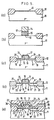
- FIG. 4 An embodiment of a semiconductor device made in accordance with the present invention is shown in Figure 4.
- Field oxide films 12 are provided on a p- type silicon substrate 11.
- Gate oxide layer 16 is formed on silicon substrate 11 and gate electrode 15 is formed on layer 16.
- gate electrode 15 is formed of polysilicon or a combination of polysilicon with a layer of a metal silicide.
- a conductive titanium nitrate layer (TiN) 17 which has an oxidation rate much slower than that of the gate electrode, is formed on the gate electrode 15. Titanium nitride is selected because it is essentially oxidation proof and forms a very stable layer.
- first and second oxide layers for example, thermal oxide layers 24, 25 are provided on the semiconductor device but are not formed on titanium nitride layer 17.
- Oxide layer 24 is located on the lateral faces of gate electrode 15 and oxide layer 25 is located on the surface of silicon substrate 11.
- First impurity diffusion regions for example, n-type low impurity diffusion regions 18, 19 are provided under the thermal oxide layer 24 formed on the lateral face of the gate electrode 15 and in the silicon substrate 11.
- Second impurity diffusion regions whose concentration is higher than that of the first impurity regions, for example, n + type high impurity diffusion regions 20, 21 are provided under the thermal oxide layer 25 and in the silicon substrate 11.
- the source region 22 is formed from the low impurity diffusion region 18 and the high impurity diffusion region 20, and the drain region 23 from the low impurity diffusion region 19 and the high impurity diffusion region 21.
- An insulation layer 26 is provided on the field oxide films 12, the thermal oxide layers 24, 25 and the titanium nitride layer 17. Contact holes are opened and a wiring layer 27 consisting of an aluminum silicon alloy is provided on the insulation layer 26 to connect the source region 22 and the drain region 23 via the contact holes.
- a passivation layer 28 is formed on the whole upper surface of the substrate.
- field oxide films 12 of about 1.0 micron thickness and an oxide layer 13 of about 300 angstrom units thickness are first produced on a p- type silicon substrate 11.
- Boron (B) is introduced in a silicon substrate 11, for controlling the threshold voltage, by ion implantation in a dose of 2 x 10" ions cm- 2 by applying an acceleration voltage of 30 KeV.
- a polycristalline silicon layer 15 having a thickness of 4000 angstrom units and 30 ohm/ is deposited on the whole silicon substrate 11.
- a titanium nitride (TiN) layer 17 of 1000 angstrom units thickness is formed on the whole polycristalline layer 15 by the reactive sputtering method using a combination of nitrogen and argon gasses.
- the titanium nitride layer 17, the polycristalline layer 15 and the oxide layer 13 are etched by a reactive ion etching method, using a patterned resist layer 14.
- the titanium nitride layer 17, the gate electrode 15 and the gate oxide layer 16 of 1.5 micron length are thus formed.
- phosphorus (P) is introduced by ion implantation in a dose of 1 x 10 13 ions c m- 2 , by applying an acceleration voltage of 40 KeV, using the gate electrode 15 as a mask.
- first impurity diffusion regions that is n- type low impurity diffusion regions 18, 19 are formed in the substrate 11.
- First and second silicon oxide layers 24, 25 of 500 angstrom units thickness are then formed on the lateral face of the gate electrode 15 and the exposed portion of the silicon substrate 11.
- the upper face of the gate electrode 15 is not oxidized as it is covered with the titanium nitride layer 17. The overhang problem is therefore eliminated.
- arsenic (As) is introduced by ion implantation in a dose of 5 x 10" ions cm- 2 , applying an acceleration voltage of 600 KeV and using the gate electrode 15 and the silicon oxide layer 24 as a mask.
- Thermal treatment is performed at 900°C in a nitrogen atmosphere.
- the second impurity diffusion regions that is n + type high impurity diffusion regions 20, 21 of 0.2 micron depth and 50 ohm/ are formed.
- high impurity diffusion regions 20, 21 are provided at a position adjacent the low impurity diffusion regions 18, 19. In this manner, a LDD structure is produced.
- an insulating layer 26 is then deposited on the whole surface, contact holes are formed in this insulating layer 26 and the thermal oxide layer 25 and a wiring layer 27, consisting of aluminum and silicon alloy, are formed. Finally, passivation layer 28 is deposited.
- the silicon oxide layer 24 formed on the lateral face of the gate electrode 15 is used as a spacer.
- the thickness of this spacer can be accurately controlled because silicon oxide layer 24 is a thermal oxide layer. Thermal oxidation is more easily controllable than the low temperature oxidation techniques in the chemical vapor deposition methods used in the prior art. Because the uniformity of this oxide layer thickness is excellent throughout the whole wafer surface, i.e., less than a 5% variation, fluctuations in MOS transistor characteristics have been essentially eliminated.
- the process forforming the spacer is much simpler than processes for forming spacers revealed in the prior art.
- the resistivity of titanium nitride is 22-23 micro ohm-cm and the titanium nitride layer 17 of 100 angstrom thickness, which is formed by the usual sputtering method, has a resistivity of 100 micro ohm-cm. Therefore, when the gate electrode 15 is connected to the wiring layer, there is the added advantage that it is not necessary to remove the titanium nitride layer 17.
- the titanium nitride layer is directly deposited on the polycristalline silicon gate electrode.
- a metal layer consisting of a material selected from the group consisting of titanium (Ti), tungsten (W) and so on or a silicide compound layer consisting of TiSi 2 , WSi 2 and so on can first be formed on the polycristalline silicon layer. In this manner, the resistivity of the gate electrode decreases and it is possible to attain high speed operation.
- the titanium nitride layer in the above-mentioned embodiment can be replaced by a tungsten nitride, a tantalum nitride or the like which has a slower oxidation rate than the gate electrode material.
Landscapes
- Insulated Gate Type Field-Effect Transistor (AREA)
Claims (8)
Applications Claiming Priority (2)
| Application Number | Priority Date | Filing Date | Title |
|---|---|---|---|
| JP65428/85 | 1985-03-29 | ||
| JP60065428A JPS61224459A (ja) | 1985-03-29 | 1985-03-29 | 半導体装置およびその製造方法 |
Publications (3)
| Publication Number | Publication Date |
|---|---|
| EP0197738A2 EP0197738A2 (fr) | 1986-10-15 |
| EP0197738A3 EP0197738A3 (en) | 1986-12-30 |
| EP0197738B1 true EP0197738B1 (fr) | 1990-08-08 |
Family
ID=13286804
Family Applications (1)
| Application Number | Title | Priority Date | Filing Date |
|---|---|---|---|
| EP86302357A Expired - Lifetime EP0197738B1 (fr) | 1985-03-29 | 1986-03-27 | Méthode de fabrication d'un dispositif semiconducteur de type LDD |
Country Status (4)
| Country | Link |
|---|---|
| EP (1) | EP0197738B1 (fr) |
| JP (1) | JPS61224459A (fr) |
| KR (1) | KR890004982B1 (fr) |
| DE (1) | DE3673208D1 (fr) |
Cited By (1)
| Publication number | Priority date | Publication date | Assignee | Title |
|---|---|---|---|---|
| US7381599B2 (en) | 1993-09-20 | 2008-06-03 | Semiconductor Energy Laboratory Co., Ltd. | Semiconductor device and method for manufacturing the same |
Families Citing this family (8)
| Publication number | Priority date | Publication date | Assignee | Title |
|---|---|---|---|---|
| JP3437863B2 (ja) | 1993-01-18 | 2003-08-18 | 株式会社半導体エネルギー研究所 | Mis型半導体装置の作製方法 |
| JPH0752774B2 (ja) * | 1988-04-25 | 1995-06-05 | 日本電気株式会社 | 半導体装置 |
| JP2513023B2 (ja) * | 1988-10-24 | 1996-07-03 | 三菱電機株式会社 | 電界効果型半導体装置およびその製造方法 |
| US5153145A (en) * | 1989-10-17 | 1992-10-06 | At&T Bell Laboratories | Fet with gate spacer |
| KR960000225B1 (ko) * | 1991-08-26 | 1996-01-03 | 가부시키가이샤 한도오따이 에네루기 겐큐쇼 | 절연게이트형 반도체장치의 제작방법 |
| TW201848B (fr) * | 1991-11-08 | 1993-03-11 | Advanced Micro Devices Inc | |
| US6777763B1 (en) | 1993-10-01 | 2004-08-17 | Semiconductor Energy Laboratory Co., Ltd. | Semiconductor device and method for fabricating the same |
| JP3030368B2 (ja) | 1993-10-01 | 2000-04-10 | 株式会社半導体エネルギー研究所 | 半導体装置およびその作製方法 |
Family Cites Families (3)
| Publication number | Priority date | Publication date | Assignee | Title |
|---|---|---|---|---|
| US3899363A (en) * | 1974-06-28 | 1975-08-12 | Ibm | Method and device for reducing sidewall conduction in recessed oxide pet arrays |
| DE3268922D1 (en) * | 1981-05-04 | 1986-03-20 | Motorola Inc | Low resistivity composite metallization for semiconductor devices and method therefor |
| US4503601A (en) * | 1983-04-18 | 1985-03-12 | Ncr Corporation | Oxide trench structure for polysilicon gates and interconnects |
-
1985
- 1985-03-29 JP JP60065428A patent/JPS61224459A/ja active Pending
-
1986
- 1986-03-27 EP EP86302357A patent/EP0197738B1/fr not_active Expired - Lifetime
- 1986-03-27 DE DE8686302357T patent/DE3673208D1/de not_active Expired - Lifetime
- 1986-03-29 KR KR1019860002397A patent/KR890004982B1/ko not_active Expired
Cited By (5)
| Publication number | Priority date | Publication date | Assignee | Title |
|---|---|---|---|---|
| US7381599B2 (en) | 1993-09-20 | 2008-06-03 | Semiconductor Energy Laboratory Co., Ltd. | Semiconductor device and method for manufacturing the same |
| US7525158B2 (en) | 1993-09-20 | 2009-04-28 | Semiconductor Energy Laboratory Co., Ltd. | Semiconductor device having pixel electrode and peripheral circuit |
| US7569856B2 (en) | 1993-09-20 | 2009-08-04 | Semiconductor Energy Laboratory Co., Ltd. | Semiconductor device and method for manufacturing the same |
| US7847355B2 (en) | 1993-09-20 | 2010-12-07 | Semiconductor Energy Laboratory Co., Ltd. | Semiconductor device including transistors with silicided impurity regions |
| US8198683B2 (en) | 1993-09-20 | 2012-06-12 | Semiconductor Energy Laboratory Co., Ltd. | Semiconductor device including transistors with silicided impurity regions |
Also Published As
| Publication number | Publication date |
|---|---|
| EP0197738A2 (fr) | 1986-10-15 |
| EP0197738A3 (en) | 1986-12-30 |
| KR890004982B1 (ko) | 1989-12-02 |
| DE3673208D1 (de) | 1990-09-13 |
| JPS61224459A (ja) | 1986-10-06 |
| KR860007756A (ko) | 1986-10-17 |
Similar Documents
| Publication | Publication Date | Title |
|---|---|---|
| US4830971A (en) | Method for manufacturing a semiconductor device utilizing self-aligned contact regions | |
| US4925807A (en) | Method of manufacturing a semiconductor device | |
| US5476802A (en) | Method for forming an insulated gate field effect transistor | |
| US4808544A (en) | LDD structure containing conductive layer between gate oxide and sidewall spacer | |
| US5869377A (en) | Method of fabrication LDD semiconductor device with amorphous regions | |
| KR0144649B1 (ko) | 반도체 장치에 있어서 실리사이드막의 선택 형성법 | |
| US4384301A (en) | High performance submicron metal-oxide-semiconductor field effect transistor device structure | |
| EP0168125B1 (fr) | Couches de câblage dans des dispositifs semi-conducteurs | |
| KR100327875B1 (ko) | 복합게이트전극을갖는mos트랜지스터및그제조방법 | |
| US6281062B1 (en) | MOS semiconductor device with self-aligned punchthrough stops and method of fabrication | |
| US4503601A (en) | Oxide trench structure for polysilicon gates and interconnects | |
| US5937303A (en) | High dielectric constant gate dielectric integrated with nitrogenated gate electrode | |
| US5175118A (en) | Multiple layer electrode structure for semiconductor device and method of manufacturing thereof | |
| US5512502A (en) | Manufacturing method for semiconductor integrated circuit device | |
| US5858867A (en) | Method of making an inverse-T tungsten gate | |
| US5023679A (en) | Semiconductor device | |
| JPH04225529A (ja) | 微量の不純物を添加したドレイン(ldd)を有する集積回路構造体を製作する改良された方法 | |
| EP0054259B1 (fr) | Procédé de fabrication d'un dispositif semiconducteur du type MIS | |
| US5940725A (en) | Semiconductor device with non-deposited barrier layer | |
| KR19990027358A (ko) | 반도체 소자의 제조방법 | |
| US5543362A (en) | Process for fabricating refractory-metal silicide layers in a semiconductor device | |
| JP2668081B2 (ja) | Cmosepromメモリセルを製造する方法 | |
| EP0390509B1 (fr) | Elément semi-conducteur et procédé pour sa réalisation | |
| US5593923A (en) | Method of fabricating semiconductor device having refractory metal silicide layer on impurity region using damage implant and single step anneal | |
| KR100376235B1 (ko) | 반도체장치및그제조방법 |
Legal Events
| Date | Code | Title | Description |
|---|---|---|---|
| PUAI | Public reference made under article 153(3) epc to a published international application that has entered the european phase |
Free format text: ORIGINAL CODE: 0009012 |
|
| 17P | Request for examination filed |
Effective date: 19860408 |
|
| AK | Designated contracting states |
Kind code of ref document: A2 Designated state(s): DE FR GB |
|
| PUAL | Search report despatched |
Free format text: ORIGINAL CODE: 0009013 |
|
| AK | Designated contracting states |
Kind code of ref document: A3 Designated state(s): DE FR GB |
|
| 17Q | First examination report despatched |
Effective date: 19880927 |
|
| GRAA | (expected) grant |
Free format text: ORIGINAL CODE: 0009210 |
|
| AK | Designated contracting states |
Kind code of ref document: B1 Designated state(s): DE FR GB |
|
| REF | Corresponds to: |
Ref document number: 3673208 Country of ref document: DE Date of ref document: 19900913 |
|
| ET | Fr: translation filed | ||
| PLBE | No opposition filed within time limit |
Free format text: ORIGINAL CODE: 0009261 |
|
| STAA | Information on the status of an ep patent application or granted ep patent |
Free format text: STATUS: NO OPPOSITION FILED WITHIN TIME LIMIT |
|
| 26N | No opposition filed | ||
| PGFP | Annual fee paid to national office [announced via postgrant information from national office to epo] |
Ref country code: GB Payment date: 19970318 Year of fee payment: 12 |
|
| PGFP | Annual fee paid to national office [announced via postgrant information from national office to epo] |
Ref country code: FR Payment date: 19980310 Year of fee payment: 13 |
|
| PG25 | Lapsed in a contracting state [announced via postgrant information from national office to epo] |
Ref country code: GB Free format text: LAPSE BECAUSE OF NON-PAYMENT OF DUE FEES Effective date: 19980327 |
|
| GBPC | Gb: european patent ceased through non-payment of renewal fee |
Effective date: 19980327 |
|
| PG25 | Lapsed in a contracting state [announced via postgrant information from national office to epo] |
Ref country code: FR Free format text: LAPSE BECAUSE OF NON-PAYMENT OF DUE FEES Effective date: 19991130 |
|
| REG | Reference to a national code |
Ref country code: FR Ref legal event code: ST |
|
| PGFP | Annual fee paid to national office [announced via postgrant information from national office to epo] |
Ref country code: DE Payment date: 20050324 Year of fee payment: 20 |