EP0198040B1 - Nichtflüchtige speicherzelle - Google Patents
Nichtflüchtige speicherzelle Download PDFInfo
- Publication number
- EP0198040B1 EP0198040B1 EP85905302A EP85905302A EP0198040B1 EP 0198040 B1 EP0198040 B1 EP 0198040B1 EP 85905302 A EP85905302 A EP 85905302A EP 85905302 A EP85905302 A EP 85905302A EP 0198040 B1 EP0198040 B1 EP 0198040B1
- Authority
- EP
- European Patent Office
- Prior art keywords
- floating gate
- write
- layer
- polysilicon
- region
- Prior art date
- Legal status (The legal status is an assumption and is not a legal conclusion. Google has not performed a legal analysis and makes no representation as to the accuracy of the status listed.)
- Expired
Links
- 238000007667 floating Methods 0.000 claims abstract description 57
- 229910021420 polycrystalline silicon Inorganic materials 0.000 claims abstract description 42
- 229920005591 polysilicon Polymers 0.000 claims abstract description 41
- 229910052581 Si3N4 Inorganic materials 0.000 claims abstract description 18
- HQVNEWCFYHHQES-UHFFFAOYSA-N silicon nitride Chemical compound N12[Si]34N5[Si]62N3[Si]51N64 HQVNEWCFYHHQES-UHFFFAOYSA-N 0.000 claims abstract description 17
- 239000000758 substrate Substances 0.000 claims abstract description 16
- XUIMIQQOPSSXEZ-UHFFFAOYSA-N Silicon Chemical compound [Si] XUIMIQQOPSSXEZ-UHFFFAOYSA-N 0.000 claims abstract description 5
- 229910052710 silicon Inorganic materials 0.000 claims abstract description 4
- 239000010703 silicon Substances 0.000 claims abstract description 4
- 230000000694 effects Effects 0.000 claims description 3
- 238000012546 transfer Methods 0.000 claims description 3
- 239000003990 capacitor Substances 0.000 abstract description 11
- 238000012986 modification Methods 0.000 abstract description 2
- 230000004048 modification Effects 0.000 abstract description 2
- 239000004065 semiconductor Substances 0.000 abstract 1
- VYPSYNLAJGMNEJ-UHFFFAOYSA-N Silicium dioxide Chemical compound O=[Si]=O VYPSYNLAJGMNEJ-UHFFFAOYSA-N 0.000 description 8
- 238000009792 diffusion process Methods 0.000 description 6
- 150000004767 nitrides Chemical class 0.000 description 5
- 230000008878 coupling Effects 0.000 description 4
- 238000010168 coupling process Methods 0.000 description 4
- 238000005859 coupling reaction Methods 0.000 description 4
- 235000012239 silicon dioxide Nutrition 0.000 description 4
- 239000000377 silicon dioxide Substances 0.000 description 4
- 230000005641 tunneling Effects 0.000 description 4
- 239000004020 conductor Substances 0.000 description 3
- 238000010276 construction Methods 0.000 description 3
- 238000000034 method Methods 0.000 description 3
- 230000015556 catabolic process Effects 0.000 description 2
- 230000005684 electric field Effects 0.000 description 2
- 238000005516 engineering process Methods 0.000 description 2
- XUFQPHANEAPEMJ-UHFFFAOYSA-N famotidine Chemical compound NC(N)=NC1=NC(CSCCC(N)=NS(N)(=O)=O)=CS1 XUFQPHANEAPEMJ-UHFFFAOYSA-N 0.000 description 2
- 238000012545 processing Methods 0.000 description 2
- 238000013459 approach Methods 0.000 description 1
- 230000002457 bidirectional effect Effects 0.000 description 1
- 230000015572 biosynthetic process Effects 0.000 description 1
- 239000013078 crystal Substances 0.000 description 1
- 230000001351 cycling effect Effects 0.000 description 1
- 230000002708 enhancing effect Effects 0.000 description 1
- 230000014509 gene expression Effects 0.000 description 1
- 238000002347 injection Methods 0.000 description 1
- 239000007924 injection Substances 0.000 description 1
- 239000012212 insulator Substances 0.000 description 1
- 230000001678 irradiating effect Effects 0.000 description 1
- 238000004519 manufacturing process Methods 0.000 description 1
- 230000003647 oxidation Effects 0.000 description 1
- 238000007254 oxidation reaction Methods 0.000 description 1
Images


Classifications
-
- H—ELECTRICITY
- H10—SEMICONDUCTOR DEVICES; ELECTRIC SOLID-STATE DEVICES NOT OTHERWISE PROVIDED FOR
- H10D—INORGANIC ELECTRIC SEMICONDUCTOR DEVICES
- H10D30/00—Field-effect transistors [FET]
- H10D30/60—Insulated-gate field-effect transistors [IGFET]
- H10D30/68—Floating-gate IGFETs
- H10D30/681—Floating-gate IGFETs having only two programming levels
- H10D30/682—Floating-gate IGFETs having only two programming levels programmed by injection of carriers through a conductive insulator, e.g. Poole-Frankel conduction
-
- G—PHYSICS
- G11—INFORMATION STORAGE
- G11C—STATIC STORES
- G11C16/00—Erasable programmable read-only memories
- G11C16/02—Erasable programmable read-only memories electrically programmable
- G11C16/04—Erasable programmable read-only memories electrically programmable using variable threshold transistors, e.g. FAMOS
- G11C16/0408—Erasable programmable read-only memories electrically programmable using variable threshold transistors, e.g. FAMOS comprising cells containing floating gate transistors
- G11C16/0433—Erasable programmable read-only memories electrically programmable using variable threshold transistors, e.g. FAMOS comprising cells containing floating gate transistors comprising cells containing a single floating gate transistor and one or more separate select transistors
-
- H—ELECTRICITY
- H10—SEMICONDUCTOR DEVICES; ELECTRIC SOLID-STATE DEVICES NOT OTHERWISE PROVIDED FOR
- H10B—ELECTRONIC MEMORY DEVICES
- H10B69/00—Erasable-and-programmable ROM [EPROM] devices not provided for in groups H10B41/00 - H10B63/00, e.g. ultraviolet erasable-and-programmable ROM [UVEPROM] devices
Definitions
- the first generation of floating gate programmable ROMs were poly (polycrystalline silicon) structures which were programmed by driving the drain junction to avalanche breakdown to generate so-called "hot" electrons which have sufficient energy to tunnel through the thick gate oxide between the drain and the isolated floating gate.
- These devices were termed FAMOS as an acronym for their floating gate, avalanche injection MOS characteristics.
- FAMOS devices which are members of the class of devices known as electrically programmable ROMs, are erased by irradiating the device with ultraviolet light.
- the second generation of programmable ROMs include electrically erasable (EEPROM) devices.
- EEPROM technology includes both two-level and three-level structures.
- the second-level polysilicon control gate is capacitively coupled to the underlying gate of a floating gate MOS transistor structure during electrical writing and erasing.
- the floating gate can be written by applying high voltage to the control gate and ground to the underlying drain. The cell is erased by reversing the polarities.
- the known memory cell is a three-level poly EEPROM structure.
- the first level poly layer includes a reference/ground conductor
- the second layer poly includes the floating gate
- the third level poly includes a programming/erase electrode.
- the reference conductor and the floating gate are processed to have upper surface regions containing asperities. These regions generate small currents at locally high electric fields which are sufficient for tunneling charge between the conductors.
- This structure provides an efficient floating gate cell in terms of size and density.
- Fig. 1 there is shown schematically a version of a three-level nonvolatile memory cell which is disclosed in the aforementioned U.S. Patent No. 4,274,012.
- the cell 10 features a diffused bias electrode which is used to effect programming and erasing by capacitive coupling.
- the relevant elements of the cell include the n+ bias electrode 15 formed in p-type substrate 11, and the overlying, stacked three-layer sandwich elements comprising program electrode 12, floating gate 13 and store/erase electrode 14. Regions 16 and 17 of asperities are formed on the upper surfaces of the program electrode 12 and the floating gate 13 for creating the localized electric fields which permit tunneling through the relatively thick oxide regions 18 and 19.
- the asperities may be produced by oxidation of the polysilicon. The use of the asperities to enhance tunneling characteristics avoids the necessity of forming thin tunneling oxide layers in large volume commercial production operations.
- program electrode 12 and transistor gate 20 are set at system ground, V ss , and a positive high voltage +V w is applied to the store/erase gate electrode 14.
- the program voltage is capacitively coupled via the electrically-floating bias electrode 15 to the floating gate 13, thereby causing electrons to tunnel from the low-potential program plate 12.
- V ss is applied to the bit line 21 and the associated transistor 20 is turned on to connect the V ss low potential bit line 21 to the bias electrode 15 so that the floating gate 13 is held at V ss by capacitive coupling.
- the positive write voltage, +V w is applied to the store/erase electrode 14 to tunnel electrons from the low potential floating gate 13 to the store/erase electrode 14.
- the known cell has the advantage of a "direct-write" capability, that is, the cell can be directly written to selected high and low threshold states.
- an electrically programmable nonvolatile memory cell of the kind specified comprises first and second write electrodes being in capacitive relationship with said floating gate through respective first and second dielectric layers selected from silicon nitride and silicon oxynitride.
- a nonvolatile memory cell according to the invention has the advantage of a simple, two-level polysilicon structure.
- a further advantage of the invention is the provision of a simplified direct-write EEPROM cell, that is, an EEPROM memory cell which can be written to a high or low threshold state regardless of the previous threshold state and without first erasing the cell.
- the cell has improved programming characteristics and endurance.
- the known cell can use a relatively low programming voltage generation from a single, five volt power supply.
- FIG. 2 A schematic of one embodiment 30 of the direct-write nonvolatile memory cell of the present invention is shown in Fig. 2.
- FIG. 5 A cross-section of the basic structure of the corresponding cell is shown in Fig. 5.
- "direct-write" means no erasing of the memory cell is required.
- a VT1 or a VTO threshold state can be programmed directly into the cell without first erasing.
- the cell 30 shown in Figs. 2 and 5 is formed on a p-type substrate 31.
- a highly-doped, n+ substrate diffusion control electrode 35 is formed in the substrate and a grounded reference plate/electrode 32 and a program gate/electrode 34 are formed from the first-level polysilicon.
- Overlapping floating gate 33 is formed from the second-level polysilicon. These gates are conventionally formed within, that is, electrically isolated by, silicon dioxide layer(s) 40. In a departure from conventional technology and structure, silicon nitride layers 38 and 39 are used as the dielectric between program electrode 34 and the overlying portion of the floating gate 33, and between the overlying portion of the floating gate 33 and grounded reference electrode 32. The respective electrode-nitride-electrode structures form capacitors C3 and C4, which are in the critical current conduction paths used to program the EEPROM to high and low voltage threshold states. Typically, the silicon nitride is formed to a thickness of about 10-20 nm (100-200 Angstroms) to allow Poole-Frenkel conduction.
- the circuit also includes a pair of n-channel enhancement mode transistors Q1 and Q2 and floating gate transistor Q3. Note that the transistors Q1 and Q3 are not shown in the cross-sectional view of Fig. 5. However, these transistors are constructed in conventional form and are connected to the elements shown in Fig. 5 according to the circuit schematic shown in Fig. 2.
- C 03 is the active gate capacitance of the floating gate transistor Q3.
- Two additional critical path capacitances are C1, which is formed by the silicon dioxide dielectric between bias control electrode 35 and program electrode 34; and C2, which is formed by the silicon dioxide dielectric between bias control electrode 35 and the floating gate electrode 33.
- the structure of the cells is such that C2-C1»C3-C4.
- V cc approximately +5 volts
- V w/E a voltage of about +20 volts.
- V C3 and V c4 across the critical nitride dielectric capacitors C3 and C4 are then given by:
- the voltage V C3 is given by the capacitive voltage divider relationship (1) and is a relatively large percentage of the applied programming voltage V W/E for the given capacitance values.
- the positive programming voltage V W/E pulls negative charges, electrons, off the floating gate, which is coupled to ground, V SS , by electrode 32, leaving the floating gate positively charged.
- the positive charge on the floating gate maintains floating gate transistor C 03 in the "on" state to pull the bit line low indicating threshold voltage state VTO.
- silicon nitride dielectric layers 38 and 39 are used in capacitor C 3 and C 4 . Although it is an excellent insulator, silicon nitride provides a higher current level than does silicon dioxide.
- the Poole-Frenkel conduction current through the nitride 38 requires lower program voltages than are required for conventional EEPROM programming.
- the current direction is bidirectional, depending upon the potential difference across electrodes 32/33 (or 34/33), and eliminates the third poly level which is utilized'in the cell disclosed in the aforementioned U.S. Patent No. 4,274,012.
- both the bit line and the word line are held at V cc during the program operation, while (as before) the program line is brought to the positive programming voltage, V W/E , of about +20 volts.
- V W/E positive programming voltage
- transistor Q2 With both the bit line and-the word line high, transistor Q2 will turn off as node A begins to rise above V cc due to capacitive coupling from the program line through capacitor C 1 .
- the following voltages appear across capacitors C 3 and C 4 :
- Reading of the state stored in the cell is performed by bringing the word line to V cc , bringing the read gate, where present, to V cc , holding the program line at a fixed potential and sensing by way of the bit line whether or not a conductive path exists between the bit line and ground potential.
- silicon oxynitride is a viable alternative to silicon nitride for the dielectric layers such as 38 and 39.
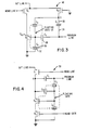
- FIG. 3 An alternative direct-write EEPROM cell 40 is shown in Fig. 3.
- Cell 40 is identical to cell 30 of Fig. 2 except that transistor Q2 is a depletion mode transistor, typically with a threshold voltage of -1 volt to -3 volts and a grounded gate. In this configuration, Q1 alone is controlled by the word line.
- the capacitive divider relationships of expressions (1 )-(4) and the method of programming described above for EEPROM cell 30 apply to the embodiment 40 as well.
- a second alternative embodiment 50 of the present direct-write EEPROM cell is shown in Fig. 4. Again, the capacitive divider relationships (1)-(4) and the programming sequence for EEPROM cell 30 apply.
- Q1 is controlled by the word line and Q2, which is controlled by the signal applied to the read gate line, is interposed between the ground reference voltage and the floating gate transistor Q3.
- the positioning of Q2 is necessary because the control electrode, node A, is an integral part of the current path between the bit line and ground during programming. The control electrode must be allowed to float during the programming sequence and Q2 allows this to happen.
- the use of silicon nitride eliminates the need for a three-layer polysilicon structure such as that used in U.S. Patent No. 4,274,012.
- the three-layer polysilicon stack structure is required in the known cell because the surface asperities can be formed only on the upper polysilicon surface. Charge can flow only from onepolysilicon layer to an overlying polysilicon layer by means of the enhanced fields associated with the textured upper surface on the lower layer. That is, electron flow is essentially unidirectional from the textured upper surface.
- current flow through the nitride is controlled by the internal nitride field and not by field emission from a textured surface.
- the current flow is not limited to one direction but rather can flow from one polysilicon layer through the silicon nitride and to a second polysilicon layer beneath it or to the single crystal substrate.
- the use of silicon nitride improves reliability because of the higher breakdown voltage of silicon nitride as compared to that of the oxide on the textured polysilicon. Also, endurance is improved because the silicon nitride conductivity is not reduced by write-erase cycling.
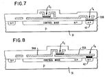
- Fig. 7 is also similar to Fig. 5 except that the ground reference electrode plate 32 is replaced by a grounded diffusion region 42.
- capacitor C4 is formed by the poly 2 floating gate, silicon nitride layer 39B and the diffusion line 42. The choice between the structures in Fig. 5 and Fig. 7 would be dictated typically by cell layout considerations.
- Fig. 8 is essentially a combination of the structures of Figs. 6 and 7 in which the program electrode 34A is part of the second polysilicon layer, the floating gate 33A is part of the first polysilicon layer, and the grounded reference electrode is formed by substrate diffusion line 42.
Landscapes
- Engineering & Computer Science (AREA)
- Microelectronics & Electronic Packaging (AREA)
- Non-Volatile Memory (AREA)
- Semiconductor Memories (AREA)
- Read Only Memory (AREA)
Claims (6)
Applications Claiming Priority (2)
| Application Number | Priority Date | Filing Date | Title |
|---|---|---|---|
| US06/665,874 US4616245A (en) | 1984-10-29 | 1984-10-29 | Direct-write silicon nitride EEPROM cell |
| US665874 | 1991-03-07 |
Publications (2)
| Publication Number | Publication Date |
|---|---|
| EP0198040A1 EP0198040A1 (de) | 1986-10-22 |
| EP0198040B1 true EP0198040B1 (de) | 1989-01-18 |
Family
ID=24671909
Family Applications (1)
| Application Number | Title | Priority Date | Filing Date |
|---|---|---|---|
| EP85905302A Expired EP0198040B1 (de) | 1984-10-29 | 1985-10-21 | Nichtflüchtige speicherzelle |
Country Status (5)
| Country | Link |
|---|---|
| US (1) | US4616245A (de) |
| EP (1) | EP0198040B1 (de) |
| JP (1) | JPH0770626B2 (de) |
| DE (1) | DE3567773D1 (de) |
| WO (1) | WO1986002779A1 (de) |
Families Citing this family (24)
| Publication number | Priority date | Publication date | Assignee | Title |
|---|---|---|---|---|
| US5172196A (en) * | 1984-11-26 | 1992-12-15 | Kabushiki Kaisha Toshiba | Nonvolatile semiconductor memory device |
| US4769788A (en) * | 1986-09-22 | 1988-09-06 | Ncr Corporation | Shared line direct write nonvolatile memory cell array |
| USRE37308E1 (en) * | 1986-12-22 | 2001-08-07 | Stmicroelectronics S.R.L. | EEPROM memory cell with a single level of polysilicon programmable and erasable bit by bit |
| IT1199828B (it) * | 1986-12-22 | 1989-01-05 | Sgs Microelettronica Spa | Cella di memoria eeprom a singolo livello di polisilicio scrivibile e cancellabile bit a bit |
| US4924278A (en) * | 1987-06-19 | 1990-05-08 | Advanced Micro Devices, Inc. | EEPROM using a merged source and control gate |
| US5166904A (en) * | 1988-02-05 | 1992-11-24 | Emanuel Hazani | EEPROM cell structure and architecture with increased capacitance and with programming and erase terminals shared between several cells |
| US5332914A (en) * | 1988-02-05 | 1994-07-26 | Emanuel Hazani | EEPROM cell structure and architecture with increased capacitance and with programming and erase terminals shared between several cells |
| US5162247A (en) * | 1988-02-05 | 1992-11-10 | Emanuel Hazani | Process for trench-isolated self-aligned split-gate EEPROM transistor and memory array |
| US5324677A (en) * | 1988-06-15 | 1994-06-28 | Seiko Instruments Inc. | Method of making memory cell and a peripheral circuit |
| US4935648A (en) * | 1988-06-15 | 1990-06-19 | Advance Micro Devices, Inc. | Optimized E2 pal cell for minimum read disturb |
| US5168464A (en) * | 1989-11-29 | 1992-12-01 | Ncr Corporation | Nonvolatile differential memory device and method |
| US5057446A (en) * | 1990-08-06 | 1991-10-15 | Texas Instruments Incorporated | Method of making an EEPROM with improved capacitive coupling between control gate and floating gate |
| US5253196A (en) * | 1991-01-09 | 1993-10-12 | The United States Of America As Represented By The Secretary Of The Navy | MOS analog memory with injection capacitors |
| US5301150A (en) * | 1992-06-22 | 1994-04-05 | Intel Corporation | Flash erasable single poly EPROM device |
| DE69323484T2 (de) * | 1993-04-22 | 1999-08-26 | Stmicroelectronics S.R.L. | Verfahren und Schaltung zur Tunneleffektprogrammierung eines MOSFETs mit schwebendem Gatter |
| JP3297173B2 (ja) | 1993-11-02 | 2002-07-02 | 三菱電機株式会社 | 半導体記憶装置およびその製造方法 |
| JP3344598B2 (ja) * | 1993-11-25 | 2002-11-11 | 株式会社デンソー | 半導体不揮発メモリ装置 |
| JPH08203884A (ja) * | 1995-01-31 | 1996-08-09 | Mitsubishi Electric Corp | オキシナイトライド膜およびその形成方法ならびにそのオキシナイトライド膜を用いた素子分離酸化膜の形成方法 |
| US5742542A (en) * | 1995-07-03 | 1998-04-21 | Advanced Micro Devices, Inc. | Non-volatile memory cells using only positive charge to store data |
| US5811852A (en) * | 1996-01-17 | 1998-09-22 | Advanced Materials Engineering Research, Inc. | Memory cell structure fabricated with improved fabrication process by forming dielectric layer directly on an insulated surface of a substrate |
| EP0904588B1 (de) * | 1996-06-14 | 2001-07-25 | Infineon Technologies AG | Anordnung und verfahren zum speichern und lesen von mehrpegelladung |
| US7508028B2 (en) * | 2006-10-26 | 2009-03-24 | Episil Technologies Inc. | Non-volatile memory |
| US8320191B2 (en) | 2007-08-30 | 2012-11-27 | Infineon Technologies Ag | Memory cell arrangement, method for controlling a memory cell, memory array and electronic device |
| US8426906B2 (en) * | 2008-04-18 | 2013-04-23 | Macronix International Co., Ltd. | Method and structure for a semiconductor charge storage device |
Family Cites Families (10)
| Publication number | Priority date | Publication date | Assignee | Title |
|---|---|---|---|---|
| JPS5236475A (en) * | 1975-09-17 | 1977-03-19 | Sanyo Electric Co Ltd | Non-volatile semiconductor memory |
| US4099196A (en) * | 1977-06-29 | 1978-07-04 | Intel Corporation | Triple layer polysilicon cell |
| US4486769A (en) * | 1979-01-24 | 1984-12-04 | Xicor, Inc. | Dense nonvolatile electrically-alterable memory device with substrate coupling electrode |
| GB2042296B (en) * | 1979-01-24 | 1983-05-11 | Xicor Inc | Nonvolatile static random access/memory device |
| US4314265A (en) * | 1979-01-24 | 1982-02-02 | Xicor, Inc. | Dense nonvolatile electrically-alterable memory devices with four layer electrodes |
| US4300212A (en) * | 1979-01-24 | 1981-11-10 | Xicor, Inc. | Nonvolatile static random access memory devices |
| CH631287A5 (fr) * | 1979-03-14 | 1982-07-30 | Centre Electron Horloger | Element de memoire non-volatile, electriquement reprogrammable. |
| JPS56134775A (en) * | 1980-03-26 | 1981-10-21 | Sanyo Electric Co Ltd | Semiconductor non-volatile memory element |
| US4334292A (en) * | 1980-05-27 | 1982-06-08 | International Business Machines Corp. | Low voltage electrically erasable programmable read only memory |
| US4404577A (en) * | 1980-06-30 | 1983-09-13 | International Business Machines Corp. | Electrically alterable read only memory cell |
-
1984
- 1984-10-29 US US06/665,874 patent/US4616245A/en not_active Expired - Lifetime
-
1985
- 1985-10-21 DE DE8585905302T patent/DE3567773D1/de not_active Expired
- 1985-10-21 EP EP85905302A patent/EP0198040B1/de not_active Expired
- 1985-10-21 JP JP60504620A patent/JPH0770626B2/ja not_active Expired - Lifetime
- 1985-10-21 WO PCT/US1985/002043 patent/WO1986002779A1/en not_active Ceased
Also Published As
| Publication number | Publication date |
|---|---|
| DE3567773D1 (en) | 1989-02-23 |
| US4616245A (en) | 1986-10-07 |
| EP0198040A1 (de) | 1986-10-22 |
| JPS62500625A (ja) | 1987-03-12 |
| WO1986002779A1 (en) | 1986-05-09 |
| JPH0770626B2 (ja) | 1995-07-31 |
Similar Documents
| Publication | Publication Date | Title |
|---|---|---|
| US4616245A (en) | Direct-write silicon nitride EEPROM cell | |
| US4630086A (en) | Nonvolatile MNOS memory | |
| US6255166B1 (en) | Nonvolatile memory cell, method of programming the same and nonvolatile memory array | |
| US4412311A (en) | Storage cell for nonvolatile electrically alterable memory | |
| US6804149B2 (en) | Nonvolatile memory cell, operating method of the same and nonvolatile memory array | |
| US6388293B1 (en) | Nonvolatile memory cell, operating method of the same and nonvolatile memory array | |
| US4334292A (en) | Low voltage electrically erasable programmable read only memory | |
| US4558344A (en) | Electrically-programmable and electrically-erasable MOS memory device | |
| EP0042964B1 (de) | Speichermatrix mit Ein-Transistor-MOS-Zellen mit schwebendem Gate | |
| EP0295935A1 (de) | Elektrisch löschbarer und programmierbarer Nur-Lese-Speicher | |
| US20110267903A1 (en) | Semiconductor memory device having dram cell mode and non-volatile memory cell mode and operation method thereof | |
| EP0051158A1 (de) | Elektrisch änderbarer Speicher mit doppelter Dichte | |
| US4713677A (en) | Electrically erasable programmable read only memory cell including trench capacitor | |
| US4479203A (en) | Electrically erasable programmable read only memory cell | |
| KR100346021B1 (ko) | 불휘발성반도체메모리 | |
| US4590503A (en) | Electrically erasable programmable read only memory | |
| US4486859A (en) | Electrically alterable read-only storage cell and method of operating same | |
| US6528845B1 (en) | Non-volatile semiconductor memory cell utilizing trapped charge generated by channel-initiated secondary electron injection | |
| KR100241524B1 (ko) | 플래쉬 메모리 셀 | |
| KR20000029662A (ko) | 비휘발성메모리셀 | |
| KR20000035785A (ko) | 비휘발성 메모리 셀 | |
| US6642571B2 (en) | Nonvolatile semiconductor memory | |
| KR100488583B1 (ko) | 듀얼비트게이트분리형플래쉬메모리소자및그의구동방법 | |
| JPS63306598A (ja) | 不揮発性メモリセルの消去方式 | |
| EP0176714B1 (de) | Speicherzelle zum Speichern logischer Daten in flüchtiger und nichtflüchtiger Weise |
Legal Events
| Date | Code | Title | Description |
|---|---|---|---|
| PUAI | Public reference made under article 153(3) epc to a published international application that has entered the european phase |
Free format text: ORIGINAL CODE: 0009012 |
|
| AK | Designated contracting states |
Kind code of ref document: A1 Designated state(s): DE GB NL |
|
| 17P | Request for examination filed |
Effective date: 19861014 |
|
| DET | De: translation of patent claims | ||
| 17Q | First examination report despatched |
Effective date: 19880518 |
|
| GRAA | (expected) grant |
Free format text: ORIGINAL CODE: 0009210 |
|
| AK | Designated contracting states |
Kind code of ref document: B1 Designated state(s): DE GB NL |
|
| REF | Corresponds to: |
Ref document number: 3567773 Country of ref document: DE Date of ref document: 19890223 |
|
| PLBE | No opposition filed within time limit |
Free format text: ORIGINAL CODE: 0009261 |
|
| STAA | Information on the status of an ep patent application or granted ep patent |
Free format text: STATUS: NO OPPOSITION FILED WITHIN TIME LIMIT |
|
| 26N | No opposition filed | ||
| REG | Reference to a national code |
Ref country code: GB Ref legal event code: 732E |
|
| NLS | Nl: assignments of ep-patents |
Owner name: NCR INTERNATIONAL INC. TE DAYTON, OHIO, VER. ST. V |
|
| NLT1 | Nl: modifications of names registered in virtue of documents presented to the patent office pursuant to art. 16 a, paragraph 1 |
Owner name: AT&T GLOBAL INFORMATION SOLUTIONS INTERNATIONAL IN |
|
| REG | Reference to a national code |
Ref country code: GB Ref legal event code: 732E |
|
| REG | Reference to a national code |
Ref country code: GB Ref legal event code: 732E |
|
| NLS | Nl: assignments of ep-patents |
Owner name: AT&T GLOBAL INFORMATION SOLUTIONS INTERNATIONAL IN |
|
| NLS | Nl: assignments of ep-patents |
Owner name: AT&T GLOBAL INFORMATION SOLUTIONS INTERNATIONAL IN |
|
| NLT1 | Nl: modifications of names registered in virtue of documents presented to the patent office pursuant to art. 16 a, paragraph 1 |
Owner name: NCR INTERNATIONAL, INC;HYUNDAI ELECTRONICS AMERICA |
|
| NLT1 | Nl: modifications of names registered in virtue of documents presented to the patent office pursuant to art. 16 a, paragraph 1 |
Owner name: NCR INTERNATIONAL, INC;HYUNDAI ELECTRONICS AMERICA |
|
| REG | Reference to a national code |
Ref country code: GB Ref legal event code: IF02 |
|
| PGFP | Annual fee paid to national office [announced via postgrant information from national office to epo] |
Ref country code: NL Payment date: 20041003 Year of fee payment: 20 |
|
| PGFP | Annual fee paid to national office [announced via postgrant information from national office to epo] |
Ref country code: DE Payment date: 20041014 Year of fee payment: 20 |
|
| PGFP | Annual fee paid to national office [announced via postgrant information from national office to epo] |
Ref country code: GB Payment date: 20041020 Year of fee payment: 20 |
|
| NLS | Nl: assignments of ep-patents |
Owner name: HYUNDAI ELECTRONICS AMERICA Owner name: NCR INTERNATIONAL, INC Owner name: HYNIX SEMICONDUCTOR INC. |
|
| NLT1 | Nl: modifications of names registered in virtue of documents presented to the patent office pursuant to art. 16 a, paragraph 1 |
Owner name: NCR INTERNATIONAL, INC Owner name: HYNIX SEMICONDUCTOR AMERICA INC. |
|
| REG | Reference to a national code |
Ref country code: GB Ref legal event code: 732E |
|
| PG25 | Lapsed in a contracting state [announced via postgrant information from national office to epo] |
Ref country code: GB Free format text: LAPSE BECAUSE OF EXPIRATION OF PROTECTION Effective date: 20051020 |
|
| PG25 | Lapsed in a contracting state [announced via postgrant information from national office to epo] |
Ref country code: NL Free format text: LAPSE BECAUSE OF EXPIRATION OF PROTECTION Effective date: 20051021 |
|
| REG | Reference to a national code |
Ref country code: GB Ref legal event code: PE20 |
|
| NLV7 | Nl: ceased due to reaching the maximum lifetime of a patent |
Effective date: 20051021 |