EP0199058A2 - Procédé et montage pour l'amélioration de la réception d'ondes radio - Google Patents
Procédé et montage pour l'amélioration de la réception d'ondes radio Download PDFInfo
- Publication number
- EP0199058A2 EP0199058A2 EP86103325A EP86103325A EP0199058A2 EP 0199058 A2 EP0199058 A2 EP 0199058A2 EP 86103325 A EP86103325 A EP 86103325A EP 86103325 A EP86103325 A EP 86103325A EP 0199058 A2 EP0199058 A2 EP 0199058A2
- Authority
- EP
- European Patent Office
- Prior art keywords
- phase
- signals
- oscillator
- circuit arrangement
- circuit
- Prior art date
- Legal status (The legal status is an assumption and is not a legal conclusion. Google has not performed a legal analysis and makes no representation as to the accuracy of the status listed.)
- Granted
Links
Images




Classifications
-
- H—ELECTRICITY
- H04—ELECTRIC COMMUNICATION TECHNIQUE
- H04B—TRANSMISSION
- H04B7/00—Radio transmission systems, i.e. using radiation field
- H04B7/02—Diversity systems; Multi-antenna system, i.e. transmission or reception using multiple antennas
- H04B7/04—Diversity systems; Multi-antenna system, i.e. transmission or reception using multiple antennas using two or more spaced independent antennas
- H04B7/08—Diversity systems; Multi-antenna system, i.e. transmission or reception using multiple antennas using two or more spaced independent antennas at the receiving station
- H04B7/0837—Diversity systems; Multi-antenna system, i.e. transmission or reception using multiple antennas using two or more spaced independent antennas at the receiving station using pre-detection combining
- H04B7/084—Equal gain combining, only phase adjustments
-
- H—ELECTRICITY
- H04—ELECTRIC COMMUNICATION TECHNIQUE
- H04B—TRANSMISSION
- H04B7/00—Radio transmission systems, i.e. using radiation field
- H04B7/02—Diversity systems; Multi-antenna system, i.e. transmission or reception using multiple antennas
- H04B7/04—Diversity systems; Multi-antenna system, i.e. transmission or reception using multiple antennas using two or more spaced independent antennas
- H04B7/08—Diversity systems; Multi-antenna system, i.e. transmission or reception using multiple antennas using two or more spaced independent antennas at the receiving station
- H04B7/0837—Diversity systems; Multi-antenna system, i.e. transmission or reception using multiple antennas using two or more spaced independent antennas at the receiving station using pre-detection combining
- H04B7/0842—Weighted combining
- H04B7/0848—Joint weighting
- H04B7/0851—Joint weighting using training sequences or error signal
-
- H—ELECTRICITY
- H04—ELECTRIC COMMUNICATION TECHNIQUE
- H04B—TRANSMISSION
- H04B7/00—Radio transmission systems, i.e. using radiation field
- H04B7/02—Diversity systems; Multi-antenna system, i.e. transmission or reception using multiple antennas
- H04B7/04—Diversity systems; Multi-antenna system, i.e. transmission or reception using multiple antennas using two or more spaced independent antennas
- H04B7/08—Diversity systems; Multi-antenna system, i.e. transmission or reception using multiple antennas using two or more spaced independent antennas at the receiving station
- H04B7/0837—Diversity systems; Multi-antenna system, i.e. transmission or reception using multiple antennas using two or more spaced independent antennas at the receiving station using pre-detection combining
- H04B7/0842—Weighted combining
- H04B7/0848—Joint weighting
- H04B7/0857—Joint weighting using maximum ratio combining techniques, e.g. signal-to- interference ratio [SIR], received signal strenght indication [RSS]
Definitions
- the invention is based on a method according to the preamble of the main claim.
- To improve the reception of radio waves it is already known to switch between signals received by different antennas depending on the quality of the signal. This so-called diversity reception requires quite complex reception devices.
- the object of the present invention is to improve the reception of radio signals, in particular in the VHF and UHF range, using the least possible technical outlay.
- the method according to the invention with the characterizing features of the main claim has the advantage that it is possible to derive an optimal signal from both antenna signals, for example to improve stereo reception, and that only one IF amplifier is required.
- the method according to the invention can be used particularly advantageously in receivers for vehicles in which there are constantly changing reception conditions due to the locomotion.
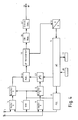
- signals received by antennas 1 and 2 pass through pre-circuits 3 and 4 to mixers 5 and 6, where they are mixed with a carrier generated by oscillator 7.
- the oscillator 7 and the pre-circuits 3 and 4 are tuned in a manner known per se with the aid of the PLL circuit 8, which in turn is controlled by a microcomputer 9, which is connected to control elements 10 and displays 11.
- the output signals of the mixers 5 and 6 (hereinafter referred to as mixed signals) are each fed via a controllable phase shifter 12 and 13 to an adder 14 which vectorially adds the mixed signals and forwards the sum signal to the IF amplifier.
- the output signal of the IF amplifier 15 is then demodulated in a manner known per se by means of an FM demodulator 16 and fed to a stereo demodulator 17.
- the LF signal can then be taken from node 23 for further amplification and reproduction.
- a limited IF signal is fed to the FM demodulator and an unlimited IF signal to an AM demodulator 18 for carrying out the method according to the invention.
- the AM demodulator 18 is used to measure the amplitude of the IF signal and thus indirectly to measure the field strength, which is the basis of the antenna signal received in each case.
- the result of the "field strength" measurement is fed to an analog-to-digital converter 21, which supplies it to the microcomputer 9 as a digital signal.
- the microcomputer changes the phase relationship of the mixed signals to each other. If the output signal of the AM demodulator 18 then becomes smaller, the phase positions are shifted in the other direction and the "field strength" then obtained is measured again. After the phase position between the mixed signals has been optimized by such an iteration, the amplitudes are optimized in a similar manner. These steps are defined in the microcomputer 9 as a program.
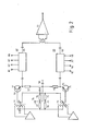
- the circuits 5, 6 and 12 to 14 are shown in more detail. Since the mixers 5 and 6 are known per se, only the push-pull output transformers 25, 26, two resistors 27, 28 for the primary-side voltage supply and a filter capacitor 29 were shown in more detail.
- a transistor 30, 31 is used as an impedance converter, each with a load resistor 32, 33.
- a voltage divider from the resistors 34, 35 is used, which between @chen the positive operating voltage and ground potential supplied at 36 is switched. Furthermore, a positive operating voltage supplied at 37 is blocked by a capacitor 38.
- the phase shifters 12 and 13 are supplied with digital control signals via the inputs 41 to 48.
- the phase rotation is brought about by controllable delay lines, each of which has a signal transit time of 4 to approximately 52 ns.
- the phase of the mixed signals can be adjusted in stages by selecting the binary default value.
- the phase-shifted mixed signals are then available at the outputs 49 and 50 of the phase shifters 12 and 13. The amount of the vectorial difference of these signals is then amplified in the operational amplifier 51.
- Digitally controllable delay lines available on the market such as those sold by Data Delay Devices Inc, USA under the designation PDU-1316, can be used as phase rotators 12, 13.
- FIGS. 3 a) to g) each represent vectorially the IF components of the output signals of mixers 5 and 6 - in each case in 4 different phase positions in accordance with the setting of phase rotators 12 and 13.
- the signals A and B already have a phase angle of 180 ° to one another in the case of in-phase antenna signals due to the switching of the transmitters 25, 26.
- the desired addition ultimately results from the subtraction at the inputs of the operational amplifier 51 (FIG. 2).
- the amount of the sum vector thus results from the connecting line of the respective arrow heads.
- the IF components A and B of the mixed signals are each shown in four different phase positions, which are achieved by correspondingly controlling the phase rotating elements 12 and 13.
- the representation presupposes in-phase antenna signals, so that the signals A and B are phase-shifted by 180 ° with the same setting of the phase rotating elements 12 and 13. It is assumed that the signals A2 and B4 are forwarded to the adder 14 at the moment shown. The remaining signals are therefore drawn in dashed lines.
- the microcomputer 9 (FIG. 1) checks whether a better reception can be achieved with a different setting.
- the phase shifter 12 is influenced, as shown in line b). Instead of signal A2, signal A1 is passed to adder 14. The phase of signal A is thus rotated in the positive direction. As can be seen from the arrowheads moving closer together, the magnitude of the sum vector and thus the amplitude of the IF signal become smaller. This is communicated to the computer via the AM demodulator 18, the sample and hold circuit 19 and the analog-to-digital converter 21 (FIG. 1). Then he changes the direction of the switching of the phase rotator 12, so that the conditions shown in line c) result. The amount of the sum vector has risen again.
- the microcomputer 9 checks from time to time whether this setting still leads to an optimal reception result. If the signals received by antennas 1 and 2 then have a different delay time difference, phase rotators 12 and 13 are automatically set differently. In order to avoid incorrect control, several "field strength" measurements lead to phase switching.
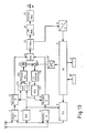
- the circuit arrangement according to FIG. 4 is constructed similarly to the circuit arrangement according to FIG. 1. However, there is a difference. Since only the relative phase relationship to one another is important for the superimposition of the two mixed signals, in the exemplary embodiment according to FIG. 4 only one controllable phase rotating element 62 is provided, which is controlled by the microprocessor 9. Depending on the individual requirements, a phase rotating element with a constant transit time can be arranged in the branch of the antenna 1. The other elements of the circuit arrangement according to FIG. 4 correspond to those of the circuit arrangement according to FIG. 1.
- phase shifters which permit a continuous change in the transit time, that is to say the phase relationship of the mixed signals with one another. This change must not take place too quickly, otherwise interference in the LF signal will occur.
- the microprocessor 9 controls the transit time of one of the mixed signals or both mixed signals in a similar manner as was explained in connection with FIG. 3.
- phase rotators examples are shown in FIGS. 5, 6 and 7.
- the signal to be rotated in phase is fed to the circuit arrangement according to FIG. 5 via the input 65 and an input transformer 66 which has two bifilar secondary windings 67, 68.
- 3 RC elements are used for phase rotation, each consisting of a resistor 69, 70 and 71 and a capacitance variation diode 72, 73 and 74.
- the signal which is rotated in phase or changed in its transit time is taken from the connection point 75 between the resistor 70 and the capacitance variation diode 73 and fed to a field effect transistor 76.
- Both the source and the drain electrodes of the field effect transistor are connected to ground potential or the positive pole 79 of the operating voltage source via load resistors 77, 78.
- the antiphase signals thus generated are fed via a further RC element consisting of the resistor 80 and the capacitance variation diode 81 to the transistor 82 serving as an output stage, the emitter of which is connected to the positive pole 79 of the operating voltage source and the collector of which is connected to ground potential via a load resistor 83 .
- the collector of transistor 82 serves as output 84 of the circuit according to FIG. 5.
- the voltage for controlling the running time is generated by microprocessor 9 (FIG. 1, FIG. 4) via a DIA converter 85 and via two resistors 86 and 87 5 supplied to the circuit.
- the resistors 86 and 87 are dimensioned so large (for example 100 kOhm) that an all too sudden change in the running time of the circuit arrangement according to FIG. 5 is prevented.
- a coupling capacitor 88 is connected between the capacitance variation diode 81 and the base of the transistor 82.
- a phase shift of k 180 0 can be achieved with the circuit arrangement according to FIG.
- the mixed signal is also supplied via an input transformer 90 with a bifilar secondary winding 91, 92.
- a transistor 93 serves at the same time as a variable resistor and to control the capacitance variation diode 94.
- the resistor 95 serves as the load resistor.
- the base of the transistor 93 is supplied with the control voltage output by the D / A converter 97 via a further resistor 96.
- the D / A converter 97 receives corresponding digital signals via the input 98 from the microprocessor 9.
- the control electrode of a field effect transistor 99 which together with the load resistor 100 serves as an output stage, is connected via a coupling capacitor 98.
- a resistor 101 connects the control electrode of the field effect transistor 99 to ground potential.
- Thieves Driving voltage is supplied at node 102 and blocked by a capacitor 103.
- the drain electrode of the field effect transistor 99 forms the output 104 of the circuit according to FIG. 6.
- any phase difference between the two antenna signals must be compensated for.
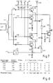
- the mixed signal to be rotated in phase is fed to the input 110 and, with the aid of an input transformer 111, which has a bifilar secondary winding, is divided into two voltages which are 180 ° out of phase with one another.
- the two connections 112 and 113 of the secondary windings of the input transformer 111 are connected to two transistors 118, 119 and 120, 121 via coupling capacitors 114, 115, 116 and 117.
- the transistors receive their base current via resistors 122, 123, 124, 125 as a function of digital control signals which are fed to the inputs 126, 127, 128 and 129 from the microprocessor 9 (FIG. 4).
- the transistors 118, 119, 120, 121 are switched to the conductive state in accordance with the digital control signals present.
- the signal from the upper end 112 of the secondary winding of the transformer 111 or the signal which is 180 ° out of phase with respect to this can therefore be passed on from the lower end 113.
- the emitters of the transistors 118, 120 are connected to one another and to the load resistor 161 and a diode 162.
- the same series circuit 163 and 164 connects the emitters of transistors 119 and 121 to ground potential.
- a voltage tapped at the upper or lower end of the secondary winding of the transformer 111 is conducted to the resistor-side connection or to the diode-side connection of an RC combination of the resistor 138 and the capacitance-variation diode 140, which are connected with two coupling capacitors 139 and 130 is connected to the transistors 118 to 121.
- the capacitance variation diode 140 receives a variable bias from the D / A converter 132 via a resistor 131, which corresponds to a digital signal supplied by the microprocessor 9 (FIG. 4) via the input 133.
- the voltage at the connection point between the resistor 138 and the capacitance variation diode 140 is amplified by the field effect transistor 134, the base voltage of which is supplied by the resistor 135, and is available at the output 136.
- the resistor 137 serves as the load resistor of the field effect transistor 134 and is connected together with the collectors of the transistors 118 to 121 to the positive pole 138 of the voltage source.
- the phase of the signal at the emitter of these two transistors is rotated by the RC element 138/140 in the sense of a lag.
- the amount of the phase shift depends on the digital signal supplied at 133.
- the signal is fed to the RC element via the capacitance variation diode 140, so that a leading phase shift occurs.
- the resistors 122 to .125 and the resistor 131 are dimensioned so large that they have a sufficient low-pass effect for the switching signals or the control voltage.
- FIG. 8 a table of the switching states of transistors 118 to 121 and their effect on the phase shift of the output voltage is shown in FIG. 8.
- Fig. 9 shows a flow chart for a program after the microcomputer 9 makes the described settings.
- the amount of the phase shift is set to 0 ° and the direction of travel is given, so the sign of the next change of the phase shift to be made.
- the measurement value M n supplied by the A / D converter 21 (FIG. 1, FIG. 4) is stored. (Program part 143).
- the index n is then increased by 1 at 144.
- the phase rotation is then increased in the program part 145 by an incremental amount PHI R.
- the size of this angle depends on the required resolution of the phase rotation.
- a value of 5.6 ° has proven itself in practice, for which purpose a bit width of 4 is required for the value to be output by the microcomputer 9 to the D / A converter 132.
- This setting is effected by outputting the corresponding binary number to the D / A converter (146).
- FIG. 10 shows a further exemplary embodiment for adapting the phase positions of the mixed signals in the sense of the invention.
- no controllable phase shifters are switched into the signal paths of the mixed signals.
- the oscillator voltage supplied to one mixer is phase-shifted in a defined manner with respect to the oscillator voltage supplied to the other mixer. As can be easily deduced, a phase shift of the oscillator voltage is communicated to the mixed product.
- the parts which are not described in more detail below correspond to those of the arrangements according to FIGS. 1 and 4.
- two controllable oscillators 7 and 151 are provided instead of one controllable oscillator 7, two controllable oscillators 7 and 151 are provided.
- the output signal of the controllable oscillator 7 is supplied on the one hand to the mixer 5 and on the other hand to a frequency divider 152.
- the output signal of the controllable oscillator 151 reaches the mixer 6 and a further, similar frequency divider 153.
- the frequency dividers 152, 153 divide the frequency of the signals fed to them by 4.
- phase discriminator 154 Their output signals are fed to the inputs of a phase discriminator 154, the output of which is via a low-pass element 155 and a PI controller 156 is routed to oscillator 151.
- a control circuit is thus formed which synchronizes the oscillator 151 with the output voltage of the oscillator 7.
- An adder circuit 157 is inserted in front of the PI controller 156, which serves to adjust the phase relationship of the two oscillator signals against one another by supplying a corresponding control voltage. The latter is specified by the microcomputer 9 via a D / A converter 158.
- phase discriminator 154 since the phase discriminator 154 only has a limited modulation range of, for example, -90 ° to + 90 °, but a larger phase rotation range of the mixed signals is required to carry out the method according to the invention, the adjustment range of the phase angle between the oscillator signals is expanded with the aid of frequency dividers 152 and 153 .
- the embodiment according to FIG. 10 has the advantage that there is no intervention in the path of the mixed signals themselves, that is to say no source of possible interference or distortion is added there.
- the control of the phase angle according to FIG. 10 results in a linear dependence of the phase angle on the control voltage, a favorable control behavior and a simple possibility of implementation.
- the method according to the invention was explained using the example of a stereo sound radio receiver. However, it is also possible to apply the method according to the invention to other receiving devices, for example to radio telephones or television receivers.
Landscapes
- Engineering & Computer Science (AREA)
- Computer Networks & Wireless Communication (AREA)
- Signal Processing (AREA)
- Variable-Direction Aerials And Aerial Arrays (AREA)
- Circuits Of Receivers In General (AREA)
- Input Circuits Of Receivers And Coupling Of Receivers And Audio Equipment (AREA)
- Burglar Alarm Systems (AREA)
Priority Applications (2)
| Application Number | Priority Date | Filing Date | Title |
|---|---|---|---|
| AT86103325T ATE91054T1 (de) | 1985-03-23 | 1986-03-12 | Verfahren und schaltungsanordnung zur verbesserung des empfangs von radiowellen. |
| EP92115650A EP0528443B1 (fr) | 1985-03-23 | 1986-03-12 | Dispositif pour la réception dans des véhicules d'ondes radio du domaine VHF |
Applications Claiming Priority (2)
| Application Number | Priority Date | Filing Date | Title |
|---|---|---|---|
| DE19853510580 DE3510580A1 (de) | 1985-03-23 | 1985-03-23 | Verfahren und schaltungsanordnung zur verbesserung des empfangs von radiowellen |
| DE3510580 | 1985-03-23 |
Related Child Applications (1)
| Application Number | Title | Priority Date | Filing Date |
|---|---|---|---|
| EP92115650.1 Division-Into | 1986-03-12 |
Publications (3)
| Publication Number | Publication Date |
|---|---|
| EP0199058A2 true EP0199058A2 (fr) | 1986-10-29 |
| EP0199058A3 EP0199058A3 (en) | 1988-08-10 |
| EP0199058B1 EP0199058B1 (fr) | 1993-06-23 |
Family
ID=6266123
Family Applications (2)
| Application Number | Title | Priority Date | Filing Date |
|---|---|---|---|
| EP86103325A Expired - Lifetime EP0199058B1 (fr) | 1985-03-23 | 1986-03-12 | Procédé et montage pour l'amélioration de la réception d'ondes radio |
| EP92115650A Expired - Lifetime EP0528443B1 (fr) | 1985-03-23 | 1986-03-12 | Dispositif pour la réception dans des véhicules d'ondes radio du domaine VHF |
Family Applications After (1)
| Application Number | Title | Priority Date | Filing Date |
|---|---|---|---|
| EP92115650A Expired - Lifetime EP0528443B1 (fr) | 1985-03-23 | 1986-03-12 | Dispositif pour la réception dans des véhicules d'ondes radio du domaine VHF |
Country Status (3)
| Country | Link |
|---|---|
| EP (2) | EP0199058B1 (fr) |
| AT (2) | ATE133303T1 (fr) |
| DE (3) | DE3510580A1 (fr) |
Cited By (8)
| Publication number | Priority date | Publication date | Assignee | Title |
|---|---|---|---|---|
| EP0227015A3 (fr) * | 1985-12-18 | 1989-02-15 | Nec Corporation | Système de réception en diversité du type de combinaison en phase |
| WO1989004092A1 (fr) * | 1987-10-31 | 1989-05-05 | Richard Hirschmann Gmbh & Co. | Procede de reception et systeme d'antennes receptrices pour la mise en oeuvre du procede |
| WO1989011184A1 (fr) * | 1988-05-03 | 1989-11-16 | Richard Hirschmann Gmbh & Co. | Procede de reception et systeme d'antennes de reception pour reception mobile |
| WO1990001246A1 (fr) * | 1988-07-26 | 1990-02-08 | Siemens Aktiengesellschaft | Procede d'acquisition d'informations sur des reseaux par un reseau numerique de transfert |
| EP0319782A3 (en) * | 1987-12-09 | 1990-09-05 | Blaupunkt-Werke Gmbh | Radio wave receiver with several antennas |
| DE4130784A1 (de) * | 1991-09-16 | 1993-03-25 | Hirschmann Richard Gmbh Co | Eichverfahren zum automatischen abgleich von diversity-systemen |
| EP1646162A1 (fr) * | 2004-09-17 | 2006-04-12 | Robert Bosch GmbH | Procédé et circuit pour la réception mobile d'un signal radio, en particulier d'un signal radio module en fréquence |
| EP2031767A2 (fr) * | 2007-08-01 | 2009-03-04 | Delphi Delco Electronics Europe GmbH | Installation de diversité d'antennes dotée de deux antennes pour la réception radio dans des véhicules |
Families Citing this family (11)
| Publication number | Priority date | Publication date | Assignee | Title |
|---|---|---|---|---|
| DE3634439A1 (de) * | 1986-10-09 | 1988-04-14 | Blaupunkt Werke Gmbh | Verfahren und schaltungsanordnung zum empfang von radiowellen |
| DE3644087A1 (de) * | 1986-12-23 | 1988-07-07 | Sennheiser Electronic | Antennendiversity-verfahren |
| DE3821714A1 (de) * | 1988-06-28 | 1990-01-04 | Telefunken Electronic Gmbh | Fernsehtuner |
| DE3926336C2 (de) * | 1989-08-09 | 2001-03-29 | Heinz Lindenmeier | Antennendiversity-Empfangsanlage zur Elimination von Empfangsstörungen beim mobilen Empfang von Fernsehsignalen |
| JP2728547B2 (ja) * | 1990-06-13 | 1998-03-18 | 株式会社日立製作所 | ダイバシティ受信装置 |
| DE4105599C1 (en) * | 1991-02-22 | 1992-09-17 | Blaupunkt-Werke Gmbh, 3200 Hildesheim, De | Diversity device for VHF car radio having several antennae - synchronises oscillator to antenna noise signals in mixer using automatic search stage and converts output of adder to carry frequency |
| DE4129830A1 (de) * | 1991-09-07 | 1993-03-25 | Blaupunkt Werke Gmbh | Ukw-empfaenger mit mehreren antennen |
| US5321850A (en) * | 1991-10-09 | 1994-06-14 | Telefonaktiebolaget L M Ericsson | Diversity radio receiver automatic frequency control |
| DE19831928A1 (de) * | 1998-07-16 | 2000-02-03 | Grundig Ag | Einrichtung zum Empfang mehrerer Rundfunksignale |
| DE19925868B4 (de) * | 1999-06-07 | 2004-10-21 | Microtune Gmbh & Co. Kg | Diversity-TV-Empfangssystem |
| DE102004002481A1 (de) | 2004-01-17 | 2005-08-11 | Robert Bosch Gmbh | Funkempfangssystem mit zwei Empfangsantennen und zwei daran angeschlossenen Empfängern |
Family Cites Families (3)
| Publication number | Priority date | Publication date | Assignee | Title |
|---|---|---|---|---|
| DE3205014A1 (de) * | 1982-02-12 | 1983-09-01 | AEG-Telefunken Nachrichtentechnik GmbH, 7150 Backnang | Phasenkorrekturschaltung in einer diversity-empfangsanlage |
| JPS5913442A (ja) * | 1982-07-14 | 1984-01-24 | Nec Corp | 信号分散最小型スペ−ス・ダイバ−シテイ−装置 |
| JPS59230334A (ja) * | 1983-06-13 | 1984-12-24 | Fujitsu Ltd | 空間ダイバ−シチ受信方式 |
-
1985
- 1985-03-23 DE DE19853510580 patent/DE3510580A1/de not_active Ceased
-
1986
- 1986-03-12 EP EP86103325A patent/EP0199058B1/fr not_active Expired - Lifetime
- 1986-03-12 AT AT92115650T patent/ATE133303T1/de not_active IP Right Cessation
- 1986-03-12 EP EP92115650A patent/EP0528443B1/fr not_active Expired - Lifetime
- 1986-03-12 DE DE3650475T patent/DE3650475D1/de not_active Expired - Fee Related
- 1986-03-12 DE DE8686103325T patent/DE3688601D1/de not_active Expired - Lifetime
- 1986-03-12 AT AT86103325T patent/ATE91054T1/de not_active IP Right Cessation
Cited By (11)
| Publication number | Priority date | Publication date | Assignee | Title |
|---|---|---|---|---|
| EP0227015A3 (fr) * | 1985-12-18 | 1989-02-15 | Nec Corporation | Système de réception en diversité du type de combinaison en phase |
| WO1989004092A1 (fr) * | 1987-10-31 | 1989-05-05 | Richard Hirschmann Gmbh & Co. | Procede de reception et systeme d'antennes receptrices pour la mise en oeuvre du procede |
| EP0321997A1 (fr) * | 1987-10-31 | 1989-06-28 | Richard Hirschmann GmbH & Co. | Procédé de réception et système d'antennes de réception pour réaliser ce procédé |
| US5204979A (en) * | 1987-10-31 | 1993-04-20 | Richard Hirschmann Gmbh & Co. | Diversity receiving method and apparatus for combining a plurality of rapidly changing signals |
| EP0319782A3 (en) * | 1987-12-09 | 1990-09-05 | Blaupunkt-Werke Gmbh | Radio wave receiver with several antennas |
| WO1989011184A1 (fr) * | 1988-05-03 | 1989-11-16 | Richard Hirschmann Gmbh & Co. | Procede de reception et systeme d'antennes de reception pour reception mobile |
| EP0344833A1 (fr) * | 1988-05-03 | 1989-12-06 | Richard Hirschmann GmbH & Co. | Méthode de réception et système d'antenne réceptrice pour réception mobile |
| WO1990001246A1 (fr) * | 1988-07-26 | 1990-02-08 | Siemens Aktiengesellschaft | Procede d'acquisition d'informations sur des reseaux par un reseau numerique de transfert |
| DE4130784A1 (de) * | 1991-09-16 | 1993-03-25 | Hirschmann Richard Gmbh Co | Eichverfahren zum automatischen abgleich von diversity-systemen |
| EP1646162A1 (fr) * | 2004-09-17 | 2006-04-12 | Robert Bosch GmbH | Procédé et circuit pour la réception mobile d'un signal radio, en particulier d'un signal radio module en fréquence |
| EP2031767A2 (fr) * | 2007-08-01 | 2009-03-04 | Delphi Delco Electronics Europe GmbH | Installation de diversité d'antennes dotée de deux antennes pour la réception radio dans des véhicules |
Also Published As
| Publication number | Publication date |
|---|---|
| EP0199058B1 (fr) | 1993-06-23 |
| DE3688601D1 (de) | 1993-07-29 |
| DE3650475D1 (de) | 1996-02-29 |
| EP0528443B1 (fr) | 1996-01-17 |
| EP0528443A2 (fr) | 1993-02-24 |
| EP0528443A3 (en) | 1993-05-05 |
| EP0199058A3 (en) | 1988-08-10 |
| ATE133303T1 (de) | 1996-02-15 |
| DE3510580A1 (de) | 1986-09-25 |
| ATE91054T1 (de) | 1993-07-15 |
Similar Documents
| Publication | Publication Date | Title |
|---|---|---|
| DE69515336T2 (de) | Mischer mit spiegelfrequenz-unterdrückung | |
| EP0528443B1 (fr) | Dispositif pour la réception dans des véhicules d'ondes radio du domaine VHF | |
| DE4420447C2 (de) | Phasenschieberschaltung und Quadraturnetzwerk | |
| DE2165911A1 (de) | Schaltung fuer den empfang amplitudenmodulierter oder frequenzmodulierter signale | |
| DE3108029C2 (de) | FM-Empfänger für ein Kraftfahrzeug | |
| DE2622594A1 (de) | Elektronischer rundfunkempfaenger | |
| DE3100557A1 (de) | Doppelueberlagerungsempfaenger | |
| DE2142660A1 (de) | Abstimm- und Empfangsfeldstärke-Anzeigeschaltung | |
| DE60022159T2 (de) | Sender mit einer geschlossenen Rückkopplung zur Modulation | |
| DE3784930T2 (de) | Empfaenger mit zwei zweigen. | |
| DE3741698A1 (de) | Empfaenger fuer radiowellen mit mehreren antennen | |
| DE3407198C2 (fr) | ||
| DE3123973C2 (de) | Phasenregelschaltung | |
| DE2624787B2 (de) | Schaltungsanordnung zur automatischen Steuerung einer Zwischenfrequenz eines FM-Empf ängers | |
| DE2658311B2 (de) | Steuerbarer Phasenschieber | |
| DE2442985C2 (fr) | ||
| DE4041345A1 (de) | Abstimmvorrichtung fuer fernsehempfaenger | |
| DE2649745C2 (de) | Frequenzsteuerbarer Oszillator | |
| DE3240565A1 (de) | Direktmischender synchronempfaenger | |
| EP1128552B1 (fr) | Circuit pour le filtrage d'un signal à haute fréquence | |
| DE4220296B4 (de) | Schaltungsanordnung zur Unterdrückung schmalbandiger Störsignale | |
| DE3412191C2 (fr) | ||
| DE3221267C2 (fr) | ||
| DE2830668C2 (fr) | ||
| DE2843977C2 (de) | Schaltungsanordnung zum Gewinnen der Tonsignale aus einem Fernsehsignal |
Legal Events
| Date | Code | Title | Description |
|---|---|---|---|
| PUAI | Public reference made under article 153(3) epc to a published international application that has entered the european phase |
Free format text: ORIGINAL CODE: 0009012 |
|
| AK | Designated contracting states |
Kind code of ref document: A2 Designated state(s): AT CH DE FR GB IT LI |
|
| RIN1 | Information on inventor provided before grant (corrected) |
Inventor name: BOCHMANN, HARALD, DR.-ING. Inventor name: HENZE, WERNER, DIPL.-ING. |
|
| PUAL | Search report despatched |
Free format text: ORIGINAL CODE: 0009013 |
|
| AK | Designated contracting states |
Kind code of ref document: A3 Designated state(s): AT CH DE FR GB IT LI |
|
| 17P | Request for examination filed |
Effective date: 19890130 |
|
| 17Q | First examination report despatched |
Effective date: 19900412 |
|
| GRAA | (expected) grant |
Free format text: ORIGINAL CODE: 0009210 |
|
| AK | Designated contracting states |
Kind code of ref document: B1 Designated state(s): AT CH DE FR GB IT LI |
|
| REF | Corresponds to: |
Ref document number: 91054 Country of ref document: AT Date of ref document: 19930715 Kind code of ref document: T |
|
| XX | Miscellaneous (additional remarks) |
Free format text: TEILANMELDUNG 92115650.1 EINGEREICHT AM 12/03/89. |
|
| ET | Fr: translation filed | ||
| GBT | Gb: translation of ep patent filed (gb section 77(6)(a)/1977) |
Effective date: 19930630 |
|
| REF | Corresponds to: |
Ref document number: 3688601 Country of ref document: DE Date of ref document: 19930729 |
|
| ITF | It: translation for a ep patent filed | ||
| PLBE | No opposition filed within time limit |
Free format text: ORIGINAL CODE: 0009261 |
|
| STAA | Information on the status of an ep patent application or granted ep patent |
Free format text: STATUS: NO OPPOSITION FILED WITHIN TIME LIMIT |
|
| 26N | No opposition filed | ||
| REG | Reference to a national code |
Ref country code: GB Ref legal event code: IF02 |
|
| PGFP | Annual fee paid to national office [announced via postgrant information from national office to epo] |
Ref country code: AT Payment date: 20030321 Year of fee payment: 18 |
|
| PGFP | Annual fee paid to national office [announced via postgrant information from national office to epo] |
Ref country code: CH Payment date: 20030325 Year of fee payment: 18 |
|
| PG25 | Lapsed in a contracting state [announced via postgrant information from national office to epo] |
Ref country code: AT Free format text: LAPSE BECAUSE OF NON-PAYMENT OF DUE FEES Effective date: 20040312 |
|
| PG25 | Lapsed in a contracting state [announced via postgrant information from national office to epo] |
Ref country code: LI Free format text: LAPSE BECAUSE OF NON-PAYMENT OF DUE FEES Effective date: 20040331 Ref country code: CH Free format text: LAPSE BECAUSE OF NON-PAYMENT OF DUE FEES Effective date: 20040331 |
|
| REG | Reference to a national code |
Ref country code: CH Ref legal event code: PL |
|
| PGFP | Annual fee paid to national office [announced via postgrant information from national office to epo] |
Ref country code: GB Payment date: 20050228 Year of fee payment: 20 |
|
| PGFP | Annual fee paid to national office [announced via postgrant information from national office to epo] |
Ref country code: FR Payment date: 20050318 Year of fee payment: 20 |
|
| PGFP | Annual fee paid to national office [announced via postgrant information from national office to epo] |
Ref country code: IT Payment date: 20050330 Year of fee payment: 20 |
|
| PGFP | Annual fee paid to national office [announced via postgrant information from national office to epo] |
Ref country code: DE Payment date: 20050513 Year of fee payment: 20 |
|
| APAH | Appeal reference modified |
Free format text: ORIGINAL CODE: EPIDOSCREFNO |
|
| PG25 | Lapsed in a contracting state [announced via postgrant information from national office to epo] |
Ref country code: GB Free format text: LAPSE BECAUSE OF EXPIRATION OF PROTECTION Effective date: 20060311 |
|
| REG | Reference to a national code |
Ref country code: GB Ref legal event code: PE20 |