EP0199424B1 - Planares Halbleiterbauteil mit einer Schutzringstruktur, Klasse solcher Bauteile und Herstellungsverfahren - Google Patents
Planares Halbleiterbauteil mit einer Schutzringstruktur, Klasse solcher Bauteile und Herstellungsverfahren Download PDFInfo
- Publication number
- EP0199424B1 EP0199424B1 EP86200696A EP86200696A EP0199424B1 EP 0199424 B1 EP0199424 B1 EP 0199424B1 EP 86200696 A EP86200696 A EP 86200696A EP 86200696 A EP86200696 A EP 86200696A EP 0199424 B1 EP0199424 B1 EP 0199424B1
- Authority
- EP
- European Patent Office
- Prior art keywords
- class
- thickness
- conductivity type
- concentration
- epitaxial layer
- Prior art date
- Legal status (The legal status is an assumption and is not a legal conclusion. Google has not performed a legal analysis and makes no representation as to the accuracy of the status listed.)
- Expired - Lifetime
Links
Images
Classifications
-
- H—ELECTRICITY
- H10—SEMICONDUCTOR DEVICES; ELECTRIC SOLID-STATE DEVICES NOT OTHERWISE PROVIDED FOR
- H10D—INORGANIC ELECTRIC SEMICONDUCTOR DEVICES
- H10D30/00—Field-effect transistors [FET]
- H10D30/60—Insulated-gate field-effect transistors [IGFET]
- H10D30/64—Double-diffused metal-oxide semiconductor [DMOS] FETs
- H10D30/66—Vertical DMOS [VDMOS] FETs
-
- H—ELECTRICITY
- H10—SEMICONDUCTOR DEVICES; ELECTRIC SOLID-STATE DEVICES NOT OTHERWISE PROVIDED FOR
- H10D—INORGANIC ELECTRIC SEMICONDUCTOR DEVICES
- H10D62/00—Semiconductor bodies, or regions thereof, of devices having potential barriers
- H10D62/10—Shapes, relative sizes or dispositions of the regions of the semiconductor bodies; Shapes of the semiconductor bodies
- H10D62/102—Constructional design considerations for preventing surface leakage or controlling electric field concentration
- H10D62/103—Constructional design considerations for preventing surface leakage or controlling electric field concentration for increasing or controlling the breakdown voltage of reverse-biased devices
- H10D62/105—Constructional design considerations for preventing surface leakage or controlling electric field concentration for increasing or controlling the breakdown voltage of reverse-biased devices by having particular doping profiles, shapes or arrangements of PN junctions; by having supplementary regions, e.g. junction termination extension [JTE]
- H10D62/106—Constructional design considerations for preventing surface leakage or controlling electric field concentration for increasing or controlling the breakdown voltage of reverse-biased devices by having particular doping profiles, shapes or arrangements of PN junctions; by having supplementary regions, e.g. junction termination extension [JTE] having supplementary regions doped oppositely to or in rectifying contact with regions of the semiconductor bodies, e.g. guard rings with PN or Schottky junctions
-
- H—ELECTRICITY
- H10—SEMICONDUCTOR DEVICES; ELECTRIC SOLID-STATE DEVICES NOT OTHERWISE PROVIDED FOR
- H10W—GENERIC PACKAGES, INTERCONNECTIONS, CONNECTORS OR OTHER CONSTRUCTIONAL DETAILS OF DEVICES COVERED BY CLASS H10
- H10W15/00—Highly-doped buried regions of integrated devices
-
- H—ELECTRICITY
- H10—SEMICONDUCTOR DEVICES; ELECTRIC SOLID-STATE DEVICES NOT OTHERWISE PROVIDED FOR
- H10W—GENERIC PACKAGES, INTERCONNECTIONS, CONNECTORS OR OTHER CONSTRUCTIONAL DETAILS OF DEVICES COVERED BY CLASS H10
- H10W15/00—Highly-doped buried regions of integrated devices
- H10W15/01—Manufacture or treatment
-
- Y—GENERAL TAGGING OF NEW TECHNOLOGICAL DEVELOPMENTS; GENERAL TAGGING OF CROSS-SECTIONAL TECHNOLOGIES SPANNING OVER SEVERAL SECTIONS OF THE IPC; TECHNICAL SUBJECTS COVERED BY FORMER USPC CROSS-REFERENCE ART COLLECTIONS [XRACs] AND DIGESTS
- Y10—TECHNICAL SUBJECTS COVERED BY FORMER USPC
- Y10S—TECHNICAL SUBJECTS COVERED BY FORMER USPC CROSS-REFERENCE ART COLLECTIONS [XRACs] AND DIGESTS
- Y10S148/00—Metal treatment
- Y10S148/013—Breakdown voltage
-
- Y—GENERAL TAGGING OF NEW TECHNOLOGICAL DEVELOPMENTS; GENERAL TAGGING OF CROSS-SECTIONAL TECHNOLOGIES SPANNING OVER SEVERAL SECTIONS OF THE IPC; TECHNICAL SUBJECTS COVERED BY FORMER USPC CROSS-REFERENCE ART COLLECTIONS [XRACs] AND DIGESTS
- Y10—TECHNICAL SUBJECTS COVERED BY FORMER USPC
- Y10S—TECHNICAL SUBJECTS COVERED BY FORMER USPC CROSS-REFERENCE ART COLLECTIONS [XRACs] AND DIGESTS
- Y10S148/00—Metal treatment
- Y10S148/07—Guard rings and cmos
Definitions
- the present invention relates to a method for producing a family of components, each semiconductor component comprising a substrate of a first type of conductivity having a high concentration of co doping, a first surface epitaxial layer of said first type of conductivity and of concentration of doping.
- c ⁇ co, an adjacent surface zone, of a second type of conductivity opposite to the first, forming with said surface epitaxial layer a main pn planar junction having over most of its surface a junction depth xj, and a structure d 'floating guard rings of said second type of conductivity and each component of the family being defined by a maximum operating voltage V.
- the invention finds a particularly advantageous application in the field of devices such as rectifying diodes, field effect transistors, bipolar transistors, thyristors, and in particular power devices operating at high voltages.
- a semiconductor component according to the above description is described in European Patent Application No. 0 115 093.
- This component consists of a junction "planar" main surrounded by guard rings to increase the breakdown voltage in the vicinity of the surface of the surface epitaxial layer deposited directly on the heavily doped substrate.
- the thickness and the concentration c of this layer are determined so that the breakdown voltage across the layer is greater than the maximum operating voltage V and also that the resistance in the on state is minimum.
- the structure of the guard rings that is to say their number, their width and their distance, is calculated, in a conventional manner, as a function of the depth xj of the main pn junction, of the concentration c of the epitaxial layer and of the desired maximum operating voltage V. This structure is reproduced on a doping mask used to simultaneously produce the main pn junction and the floating guard rings.
- each specific semiconductor component has a specific mask, which greatly increases the number of masks when a wide variety of such components are manufactured. It is the object of the present invention to provide a semiconductor component in accordance with the preamble which could be adapted to a given structure of guard rings.
- a semiconductor component comprising a substrate of a first type of conductivity having a high concentration of co doping, a first surface epitaxial layer of said first type of conductivity and concentration doping c ⁇ co, an adjacent surface area, of a second type of conductivity opposite to the first, forming with said surface epitaxial layer a main pn planar junction having over the greater part of its surface a junction depth xj, and a structure of floating guard rings of said second type of conductivity is remarkable in that between said substrate and said first epitaxial layer, is interposed a second epitaxial layer having a doping concentration c 'such that co> c'> c.
- the thickness of the surface layer, the concentration c 'of the second epitaxial layer as well as its thickness it is possible, for a given configuration of rings, to design a semiconductor component operating at the maximum operating voltage. desired and with optimal resistance to passing state.
- a family of semiconductor components of the "planar" type comprising a heavily doped substrate and a surface epitaxial layer of concentration of carriers c, in which a main pn junction of depth xj and a ring structure are produced.
- each component of the family being defined by a maximum operating voltage V, is remarkable in that, a particular structure of floating guard rings having been determined for another component of the same type, called reference component, outside the family, consisting of a single epitaxial layer of thickness e o and concentration c, and having a maximum operating voltage V m greater than that of all the components of the family, each component of the family also has, on the one hand, said particular structure of guard rings for structure of guard rings, and, on the other hand, between the substrate and the surface epitaxial layer, a second epitaxial layer of carrier concentration c ', greater than c, the sum of the thickness e of the surface epitaxial layer and the thickness e' of the second epitaxial layer being at most equal to the thickness eo.
- the invention therefore consists in defining a single ring structure for all the components of the family which can then be produced using a single mask, with the obvious industrialization advantages that this provides.
- This process has the advantage of being simple to implement since all the components of the family have the same total thickness as regards their epitaxial layers and therefore correspond to a standard epitaxy operation. However, the components obtained by this process do not have an optimal resistance R on because the total thickness eoest generally oversized, in particular for those of the components which have a low maximum operating voltage.
- a second method according to the invention is used, remarkable in that, for said reference component, in the case of a planar structure, the thickness e o and the concentration c of the single epitaxial layer so that the breakdown voltage across the layer is at least equal to the maximum operating voltage Vm and that the resistance R on in the on state is minimal, and in that, thereafter, said said is determined particular structure of floating guard rings associated with the main pn junction of depth xj, and in that, for each component of the family, we first calculate the concentration c 'and a total thickness e'o, which for a single epitaxial layer of concentration c ′ in a flat structure, make it possible to obtain a breakdown voltage at least equal to the maximum operating voltage V and a resistance Ron in the minimum on state, and in that a epa value issuer e at least equal to the distance d 1 between the main junction and the first guard ring, the thickness e 'then being taken equal to e'o e.
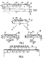
- FIG. 1 is a partial section view of a semiconductor component of the "planar" type, comprising a highly doped substrate 11, here of conductivity n +, constituting for example the drain of an MOS transistor, and a surface epitaxial layer 12 of carrier concentration c, of conductivity n in the case of FIG. 1.
- a semiconductor component of the "planar" type comprising a highly doped substrate 11, here of conductivity n +, constituting for example the drain of an MOS transistor, and a surface epitaxial layer 12 of carrier concentration c, of conductivity n in the case of FIG. 1.
- this epitaxial layer 12 are made a main pn junction 13 of depth xi and a structure 14 of floating guard rings which make it possible to avoid breakdown on the surface when the bias voltage which blocks the pn junction 13 increases, the depletion region passes successively through each of the rings before the breakdown voltage is reached.
- the surface epitaxial layer 12 is partly coated with an oxide layer 20.
- the surface area corresponding to the main junction 13 is covered with a metal electrode 21 to which a negative voltage -V is applied high relative to the layer 12 so as to polarize the pn junction 13. Additional security is obtained by means of an n + 22 ring arranged at the periphery of the crystal so as to prevent the depletion region from reaching the edge of the crystal.
- a floating electrode 23 partially covers the ring 22 and the oxide layer 20.
- the semiconductor component also comprises, between the substrate 11 and the surface epitaxial layer 12, a second epitaxial layer 15 of carrier concentration c ′.
- This configuration with two epitaxial layers of different concentrations makes it possible, by giving the concentrations and the thicknesses of the layers of adequate values, to produce a component having a given breakdown voltage and a minimum resistance to the on state Ron, when a structure d floating guard rings is imposed.
- a particular structure of floating guard rings is determined for another component of the same type, called reference component 17, outside the family, consisting of a single epitaxial layer 18 of thickness eo and of concentration c, and having a maximum operating voltage Vm greater than that of all the components of the family.
- each component 16 of the family also has, on the one hand, the particular structure of guard rings, and, on the other hand, in accordance with FIG. 1, a second epitaxial layer 15 situated between the substrate 11 and the surface layer 12.
- This second layer 15 has a concentration of carriers c ', greater than c, and its thickness e' is such that the sum e + e 'is at most equal to e ⁇ .
- FIG. 2 (a) shows a component 16 of the family produced according to a first method which consists in calculating, first, for the reference component 17, in the case of a planar structure, the thickness e o and the concentration c of the single epitaxial layer 18 so that the breakdown voltage across the layer 12 is at least equal to the maximum operating voltage V m and that the resistance Ron in the on state is minimal.
- This particular structure of floating guard rings associated with the main pn junction 13 of depth xj is then determined.
- the semiconductor component 16 of FIG. 2 (b) is obtained according to a second method in which, after having determined the concentration c and the structure of guard rings for the reference component 17 in the same way as for the first method, we first calculate, for each component 16 of the family, the concentration c 'and a total thickness e'o which, for a single epitaxial layer of concentration c' in planar structure, make it possible to obtain a breakdown voltage at least equal to the maximum operating voltage V and a minimum resistance Ron in the on state. Next, a value of the thickness e is at least equal to the distance d 1 between the main junction 13 and the first guard ring, the thickness e 'then being taken equal to e'o - e.
- This production process generally makes it possible to obtain thinner layers and therefore an even lower resistance to the passing state than by the first process.
- the total thickness of this component is 55 ⁇ m instead of 80 in the previous example and its resistance in the on state is lower.
Landscapes
- Bipolar Transistors (AREA)
- Thyristors (AREA)
Claims (2)
Applications Claiming Priority (2)
| Application Number | Priority Date | Filing Date | Title |
|---|---|---|---|
| FR8506410A FR2581252B1 (fr) | 1985-04-26 | 1985-04-26 | Composant semiconducteur du type planar a structure d'anneaux de garde, famille de tels composants et procede de realisation |
| FR8506410 | 1985-04-26 |
Publications (3)
| Publication Number | Publication Date |
|---|---|
| EP0199424A2 EP0199424A2 (de) | 1986-10-29 |
| EP0199424A3 EP0199424A3 (en) | 1987-01-21 |
| EP0199424B1 true EP0199424B1 (de) | 1990-07-11 |
Family
ID=9318733
Family Applications (1)
| Application Number | Title | Priority Date | Filing Date |
|---|---|---|---|
| EP86200696A Expired - Lifetime EP0199424B1 (de) | 1985-04-26 | 1986-04-23 | Planares Halbleiterbauteil mit einer Schutzringstruktur, Klasse solcher Bauteile und Herstellungsverfahren |
Country Status (5)
| Country | Link |
|---|---|
| US (1) | US5028548A (de) |
| EP (1) | EP0199424B1 (de) |
| JP (1) | JPH0799747B2 (de) |
| DE (1) | DE3672519D1 (de) |
| FR (1) | FR2581252B1 (de) |
Families Citing this family (28)
| Publication number | Priority date | Publication date | Assignee | Title |
|---|---|---|---|---|
| GB2201543A (en) * | 1987-02-25 | 1988-09-01 | Philips Electronic Associated | A photosensitive device |
| US5032878A (en) * | 1990-01-02 | 1991-07-16 | Motorola, Inc. | High voltage planar edge termination using a punch-through retarding implant |
| US5266831A (en) * | 1991-11-12 | 1993-11-30 | Motorola, Inc. | Edge termination structure |
| US5677562A (en) * | 1996-05-14 | 1997-10-14 | General Instrument Corporation Of Delaware | Planar P-N junction semiconductor structure with multilayer passivation |
| US6002159A (en) * | 1996-07-16 | 1999-12-14 | Abb Research Ltd. | SiC semiconductor device comprising a pn junction with a voltage absorbing edge |
| JP3632344B2 (ja) * | 1997-01-06 | 2005-03-23 | 日産自動車株式会社 | 半導体装置 |
| EP1029358A1 (de) * | 1997-11-03 | 2000-08-23 | Infineon Technologies AG | Hochspannungsfeste randstruktur für halbleiterbauelemente |
| GB2403346B (en) * | 2000-10-31 | 2005-05-11 | Fuji Electric Co Ltd | Semiconductor device |
| GB2373634B (en) * | 2000-10-31 | 2004-12-08 | Fuji Electric Co Ltd | Semiconductor device |
| JP5011611B2 (ja) | 2001-06-12 | 2012-08-29 | 富士電機株式会社 | 半導体装置 |
| DE10250608B4 (de) * | 2002-10-30 | 2005-09-29 | eupec Europäische Gesellschaft für Leistungshalbleiter mbH | Thyristorbauelement mit verbessertem Sperrverhalten in Rückwärtsrichtung |
| US7595542B2 (en) * | 2006-03-13 | 2009-09-29 | Fairchild Semiconductor Corporation | Periphery design for charge balance power devices |
| US7592668B2 (en) * | 2006-03-30 | 2009-09-22 | Fairchild Semiconductor Corporation | Charge balance techniques for power devices |
| US7541247B2 (en) * | 2007-07-16 | 2009-06-02 | International Business Machines Corporation | Guard ring structures for high voltage CMOS/low voltage CMOS technology using LDMOS (lateral double-diffused metal oxide semiconductor) device fabrication |
| US8174067B2 (en) | 2008-12-08 | 2012-05-08 | Fairchild Semiconductor Corporation | Trench-based power semiconductor devices with increased breakdown voltage characteristics |
| US8304829B2 (en) | 2008-12-08 | 2012-11-06 | Fairchild Semiconductor Corporation | Trench-based power semiconductor devices with increased breakdown voltage characteristics |
| US8227855B2 (en) * | 2009-02-09 | 2012-07-24 | Fairchild Semiconductor Corporation | Semiconductor devices with stable and controlled avalanche characteristics and methods of fabricating the same |
| US8148749B2 (en) * | 2009-02-19 | 2012-04-03 | Fairchild Semiconductor Corporation | Trench-shielded semiconductor device |
| US8049276B2 (en) * | 2009-06-12 | 2011-11-01 | Fairchild Semiconductor Corporation | Reduced process sensitivity of electrode-semiconductor rectifiers |
| JP5558393B2 (ja) * | 2011-03-10 | 2014-07-23 | 株式会社東芝 | 半導体装置 |
| JP2012195519A (ja) * | 2011-03-18 | 2012-10-11 | Kyoto Univ | 半導体素子及び半導体素子の製造方法 |
| US9129819B2 (en) * | 2011-08-05 | 2015-09-08 | Fuji Electric Co., Ltd. | Semiconductor device and method of manufacturing semiconductor device |
| US8872278B2 (en) | 2011-10-25 | 2014-10-28 | Fairchild Semiconductor Corporation | Integrated gate runner and field implant termination for trench devices |
| EP3353814B1 (de) * | 2015-11-27 | 2019-07-10 | ABB Schweiz AG | Flächeneffizienter abschluss mit schwebenden feldringen |
| US10424635B2 (en) * | 2016-04-06 | 2019-09-24 | Littelfuse, Inc. | High voltage semiconductor device with guard rings and method associated therewith |
| CN107611165A (zh) * | 2016-07-12 | 2018-01-19 | 北大方正集团有限公司 | 分压环的制备方法、分压环和功率晶体管 |
| JP7190256B2 (ja) | 2018-02-09 | 2022-12-15 | ローム株式会社 | 半導体装置 |
| US10361276B1 (en) * | 2018-03-17 | 2019-07-23 | Littelfuse, Inc. | Embedded field plate field effect transistor |
Family Cites Families (9)
| Publication number | Priority date | Publication date | Assignee | Title |
|---|---|---|---|---|
| FR2108781B1 (de) * | 1970-10-05 | 1974-10-31 | Radiotechnique Compelec | |
| JPS523277B2 (de) * | 1973-05-19 | 1977-01-27 | ||
| FR2480036A1 (fr) * | 1980-04-04 | 1981-10-09 | Thomson Csf | Structure de dispositif a semi-conducteur a anneau de garde et a fonctionnement unipolaire |
| DE3131611A1 (de) * | 1981-08-10 | 1983-02-24 | Siemens AG, 1000 Berlin und 8000 München | Epitaxialer transistor |
| US4573064A (en) * | 1981-11-02 | 1986-02-25 | Texas Instruments Incorporated | GaAs/GaAlAs Heterojunction bipolar integrated circuit devices |
| JPS5976466A (ja) * | 1982-10-25 | 1984-05-01 | Mitsubishi Electric Corp | プレ−ナ形半導体装置 |
| GB2131603B (en) * | 1982-12-03 | 1985-12-18 | Philips Electronic Associated | Semiconductor devices |
| JPS59189679A (ja) * | 1983-04-13 | 1984-10-27 | Hitachi Ltd | ダイオ−ド |
| JPS6012859A (ja) * | 1983-06-20 | 1985-01-23 | Ricoh Co Ltd | フアクシミリ・複写機・ソ−タ複合装置 |
-
1985
- 1985-04-26 FR FR8506410A patent/FR2581252B1/fr not_active Expired
-
1986
- 1986-04-23 DE DE8686200696T patent/DE3672519D1/de not_active Expired - Lifetime
- 1986-04-23 EP EP86200696A patent/EP0199424B1/de not_active Expired - Lifetime
- 1986-04-23 JP JP61092444A patent/JPH0799747B2/ja not_active Expired - Lifetime
-
1990
- 1990-06-26 US US07/544,809 patent/US5028548A/en not_active Expired - Fee Related
Also Published As
| Publication number | Publication date |
|---|---|
| EP0199424A2 (de) | 1986-10-29 |
| FR2581252B1 (fr) | 1988-06-10 |
| JPS61248555A (ja) | 1986-11-05 |
| FR2581252A1 (fr) | 1986-10-31 |
| EP0199424A3 (en) | 1987-01-21 |
| DE3672519D1 (de) | 1990-08-16 |
| JPH0799747B2 (ja) | 1995-10-25 |
| US5028548A (en) | 1991-07-02 |
Similar Documents
| Publication | Publication Date | Title |
|---|---|---|
| EP0199424A2 (de) | Planares Halbleiterbauteil mit einer Schutzringstruktur, Klasse solcher Bauteile und Herstellungsverfahren | |
| EP0021869B1 (de) | Verfahren zur Herstellung einer Schottky-Diode mit verbessertem Spannungsverhalten | |
| FR2794897A1 (fr) | Plaquette a semi-conducteur et dispositif a semi-conducteur fabrique a partir d'une telle plaquette | |
| FR2544916A1 (fr) | Procede de fabrication de transistors a effet de champ mos | |
| FR2494499A1 (fr) | Structure plane pour dispositifs semi-conducteurs a haute tension | |
| FR2738394A1 (fr) | Dispositif a semi-conducteur en carbure de silicium, et son procede de fabrication | |
| EP3114713B1 (de) | Verfahren zur erzeugung einer fotovoltaischen zelle mit selektiver dotierung | |
| EP1330836A1 (de) | Verfahren zur herstellung von einer schottky diode in siliziumkarbid | |
| FR3012256A1 (fr) | Composant de puissance vertical haute tension | |
| FR2481518A1 (fr) | Procede de realisation d'un dispositif semiconducteur comportant des transistors a effet de champ complementaires | |
| EP2795668B1 (de) | Verfahren zur herstellung eines mos-stapels auf einem diamantsubstrat | |
| EP1483793B1 (de) | Leistungs-schottkydiode mit sicoi-substrat und diesbezügliches herstellungsverfahren | |
| EP0092266A1 (de) | Verfahren zur Herstellung von Feldeffekttransistoren aus GaAs durch Ionenimplantation und nach diesem Verfahren hergestellte Transistoren | |
| FR2488734A1 (fr) | Diode zener et procede pour la fabriquer | |
| FR2673044A1 (fr) | Transistor a effet de champ comprenant une couche enterree, et procede de fabrication. | |
| FR2511194A1 (fr) | Transistor a effet de champ et procede de fabrication | |
| EP0165863A1 (de) | Verfahren zum Herstellen von mindestens einem Dünnfilm-Feldeffekttransistor und nach diesem Verfahren hergestellter Transistor | |
| CH616024A5 (de) | ||
| FR2512590A1 (fr) | Transistor a effet de champ du type a jonction et procede de fabrication | |
| EP0082787B1 (de) | Photodiode mit getrennten Absorptions- und Avalanchezonen | |
| EP0193462B1 (de) | PIN-Hochfrequenzdiode mit abrupten Übergängen | |
| EP0126499B1 (de) | Verfahren zur Herstellung eines bipolaren Transistors hoher Spannung | |
| FR2647967A1 (fr) | Dispositif optoelectronique sur substrat semi-isolant et procede de realisation d'un tel dispositif | |
| FR3011385A1 (fr) | Diode schottky en nitrure de gallium avec anneau de garde | |
| FR2572584A1 (fr) | Procede de fabrication d'un dispositif semi-conducteur a structure de grille encastree, notamment d'un transistor a induction statique |
Legal Events
| Date | Code | Title | Description |
|---|---|---|---|
| PUAI | Public reference made under article 153(3) epc to a published international application that has entered the european phase |
Free format text: ORIGINAL CODE: 0009012 |
|
| AK | Designated contracting states |
Kind code of ref document: A2 Designated state(s): DE FR GB NL |
|
| PUAL | Search report despatched |
Free format text: ORIGINAL CODE: 0009013 |
|
| AK | Designated contracting states |
Kind code of ref document: A3 Designated state(s): DE FR GB NL |
|
| 17P | Request for examination filed |
Effective date: 19870515 |
|
| 17Q | First examination report despatched |
Effective date: 19880927 |
|
| GRAA | (expected) grant |
Free format text: ORIGINAL CODE: 0009210 |
|
| RAP1 | Party data changed (applicant data changed or rights of an application transferred) |
Owner name: N.V. PHILIPS' GLOEILAMPENFABRIEKEN Owner name: PHILIPS COMPOSANTS |
|
| AK | Designated contracting states |
Kind code of ref document: B1 Designated state(s): DE FR GB NL |
|
| PG25 | Lapsed in a contracting state [announced via postgrant information from national office to epo] |
Ref country code: NL Effective date: 19900711 |
|
| REF | Corresponds to: |
Ref document number: 3672519 Country of ref document: DE Date of ref document: 19900816 |
|
| GBT | Gb: translation of ep patent filed (gb section 77(6)(a)/1977) | ||
| NLV1 | Nl: lapsed or annulled due to failure to fulfill the requirements of art. 29p and 29m of the patents act | ||
| PLBE | No opposition filed within time limit |
Free format text: ORIGINAL CODE: 0009261 |
|
| STAA | Information on the status of an ep patent application or granted ep patent |
Free format text: STATUS: NO OPPOSITION FILED WITHIN TIME LIMIT |
|
| 26N | No opposition filed | ||
| PGFP | Annual fee paid to national office [announced via postgrant information from national office to epo] |
Ref country code: GB Payment date: 19960329 Year of fee payment: 11 |
|
| PGFP | Annual fee paid to national office [announced via postgrant information from national office to epo] |
Ref country code: FR Payment date: 19960429 Year of fee payment: 11 |
|
| REG | Reference to a national code |
Ref country code: FR Ref legal event code: CD |
|
| PGFP | Annual fee paid to national office [announced via postgrant information from national office to epo] |
Ref country code: DE Payment date: 19960625 Year of fee payment: 11 |
|
| PG25 | Lapsed in a contracting state [announced via postgrant information from national office to epo] |
Ref country code: GB Effective date: 19970423 |
|
| GBPC | Gb: european patent ceased through non-payment of renewal fee |
Effective date: 19970423 |
|
| PG25 | Lapsed in a contracting state [announced via postgrant information from national office to epo] |
Ref country code: FR Free format text: LAPSE BECAUSE OF NON-PAYMENT OF DUE FEES Effective date: 19971231 |
|
| PG25 | Lapsed in a contracting state [announced via postgrant information from national office to epo] |
Ref country code: DE Free format text: LAPSE BECAUSE OF NON-PAYMENT OF DUE FEES Effective date: 19980101 |
|
| REG | Reference to a national code |
Ref country code: FR Ref legal event code: ST |